
Related Manuals for Asus AAEON GENE-APL6


Summary of Contents for Asus AAEON GENE-APL6
- Page 1 GENE-APL6 3.5” Subcompact Board User’s Manual 4 Last Updated: August 20, 2021...
- Page 2 Copyright Notice This document is copyrighted, 2021. All rights are reserved. The original manufacturer reserves the right to make improvements to the products described in this manual at any time without notice. No part of this manual may be reproduced, copied, translated, or transmitted in any form or by any means without the prior written permission of the original manufacturer.
- Page 3 Acknowledgements All other products’ name or trademarks are properties of their respective owners. Microsoft Windows is a registered trademark of Microsoft Corp. ⚫ Intel®, Pentium®, and Celeron® are registered trademarks of Intel Corporation ⚫ Intel Atom™ is a trademark of Intel Corporation ⚫...
- Page 4 Packing List Before setting up your product, please make sure the following items have been shipped: Item Quantity GENE-APL6 MB ⚫ Heat Spreader ⚫ If any of these items are missing or damaged, please contact your distributor or sales representative immediately. Preface...
- Page 5 About this Document This User’s Manual contains all the essential information, such as detailed descriptions and explanations on the product’s hardware and software features (if any), its specifications, dimensions, jumper/connector settings/definitions, and driver installation instructions (if any), to facilitate users in setting up their product. Users may refer to the product page at AAEON.com for the latest version of this document.
- Page 6 Safety Precautions Please read the following safety instructions carefully. It is advised that you keep this manual for future references All cautions and warnings on the device should be noted. Make sure the power source matches the power rating of the device. Position the power cord so that people cannot step on it.
- Page 7 If any of the following situations arises, please the contact our service personnel: Damaged power cord or plug Liquid intrusion to the device iii. Exposure to moisture Device is not working as expected or in a manner as described in this manual The device is dropped or damaged Any obvious signs of damage displayed on the device...
- Page 8 FCC Statement This device complies with Part 15 FCC Rules. Operation is subject to the following two conditions: (1) this device may not cause harmful interference, and (2) this device must accept any interference received including interference that may cause undesired operation.
- Page 9 China RoHS Requirements (CN) 产品中有毒有害物质或元素名称及含量 AAEON Main Board/ Daughter Board/ Backplane 有毒有害物质或元素 部件名称 铅 汞 镉 六价铬 多溴联苯 多溴二苯醚 (Pb) (Hg) (Cd) (Cr(VI)) (PBB) (PBDE) 印刷电路板 ○ ○ ○ ○ ○ ○ 及其电子组件 外部信号 ○ ○ ○ ○ ○ ○ 连接器及线材...
- Page 10 China RoHS Requirement (EN) Poisonous or Hazardous Substances or Elements in Products AAEON Main Board/ Daughter Board/ Backplane Poisonous or Hazardous Substances or Elements Hexavalent Polybrominated Polybrominated Component Lead Mercury Cadmium Chromium Biphenyls Diphenyl Ethers (Pb) (Hg) (Cd) (Cr(VI)) (PBB) (PBDE) PCB &...
-
Page 11: Table Of Contents
Table of Contents Chapter 1 - Product Specifications..................1 Specifications ......................2 Chapter 2 – Hardware Information ..................6 Dimensions ....................... 7 2.1.1 Dimensions (Optional HDMI SKU)............10 Jumpers and Connectors ..................13 2.2.1 Jumpers and Connectors (Optional HDMI SKU) ........14 Assembly Options .................... - Page 12 2.6.6 Audio I/O Port (CN6) ................27 2.6.7 Mini-Card Slot (Full-Size) (CN7) .............. 27 2.6.8 COM Port 2 (CN8) ..................30 2.6.9 COM Port 3 (CN9) ..................32 2.6.10 COM Port 4 (CN10) ................... 34 2.6.11 mSATA Slot (Half-Sized) (CN11) ............... 35 2.6.12 LPC Port (CN12)..................
- Page 13 AMI BIOS Setup ...................... 61 Setup Submenu: Main ..................62 Setup Submenu: Advanced ................. 63 3.4.1 Trusted Computing ..................64 3.4.2 CPU Configuration ..................66 3.4.3 SATA Configuration ................... 68 3.4.4 SCC Configuration ..................70 3.4.5 PCI Express Configuration................. 71 3.4.5.1 PCIE Slot (CN7) ................
- Page 14 Driver Download/Installation ................94 Appendix A - I/O Information ....................96 I/O Address Map ....................97 Memory Address Map ..................99 IRQ Mapping Chart ..................... 100 Appendix B – Mating Connectors ..................117 List of Mating Connectors and Cables ............. 118 Preface...
-
Page 15: Chapter 1 - Product Specifications
Chapter 1 Chapter 1 - Product Specifications... -
Page 16: Specifications
Specifications System Form Factor 3.5'' Subcompact Board Intel® Atom™/ Celeron®/ Pentium® Processor: Pentium N4200 (4C/4T, 1.10 GHz, up to 2.5 GHz) Celeron N3350 (2C/2T, 1.10 GHz, up to 2.40 GHz) Atom E3950 (4C/4T, 1.60 GHz, up to 2.00GHz) Atom E3940 (4C/4T, 1.60GHz, up to 1.80GHz) Atom E3930 (2C/2T, 1.30GHz, up to 1.80GHz) CPU TDP 6W: N4200, N3350... - Page 17 Power Power Requirement +9-36V (Optional: +12V) Power Supply Type AT/ATX Connector Phoenix 2-pin Connector Power Consumption Typical 2.36A at +12V with Intel® E3950, DDR3L 1866MHz 8GB Power Consumption Max 2.41A at +12V with Intel® E3950, DDR3L 1866MHz 8GB Display Controller Intel®...
- Page 18 External I/O Others — Internal I/O USB2.0 x 2 Serial Port COM2, COM3 (RS232/422/485, supports 5V/12V/RI) COM4 (RS232) Video LVDS1 x 1 LVDS2/HDMI x 1 (Default LVDS2) SATA SATA III x 1 +5V SATA Power Connector x 1 Audio Audio Header x 1 DIO/GPIO 8-bit SMBus/I2C...
- Page 19 Expansion — Others — Mechanical Dimensions 5.75" x 4" (146mm x 101.7mm) Environment Operating Temperature 32°F ~ 140°F (0°C ~ 60°C) Storage Temperature -40°F ~ 176°F (-40°C ~ 80°C) Operating Humidity 0% ~ 90% relative humidity, non-condensing MTBF 374,567 Certification CE/FCC Chapter 1 –...
-
Page 20: Chapter 2 - Hardware Information
Chapter 2 Chapter 2 – Hardware Information... -
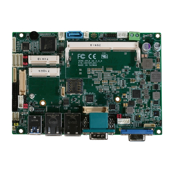
Page 21: Dimensions
Dimensions Component Side Chapter 2 – Hardware Information... - Page 22 Solder Side Chapter 2 – Hardware Information...
- Page 23 With Heat Spreader Chapter 2 – Hardware Information...
-
Page 24: Dimensions (Optional Hdmi Sku)
2.1.1 Dimensions (Optional HDMI SKU) Component Side Chapter 2 – Hardware Information... - Page 25 Solder Side Chapter 2 – Hardware Information...
- Page 26 With Heat Spreader Chapter 2 – Hardware Information...
-
Page 27: Jumpers And Connectors
Jumpers and Connectors Component Side Chapter 2 – Hardware Information... -
Page 28: Jumpers And Connectors (Optional Hdmi Sku)
2.2.1 Jumpers and Connectors (Optional HDMI SKU) Component Side Chapter 2 – Hardware Information... -
Page 29: Assembly Options
Assembly Options Optional Accessory: GENE-APL6-HSK01 Chapter 2 – Hardware Information... -
Page 30: Block Diagram
Block Diagram Chapter 2 – Hardware Information... -
Page 31: List Of Jumpers
List of Jumpers Please refer to the table below for all of the board’s jumpers that you can configure for your application Label Function Front Panel Connector COM2 Pin8 Function Selection COM3 Pin8 Function Selection LVDS Port2 Backlight Lightness Control Mode Selection LVDS Port2 Backlight Inverter VCC Selection and Operating VDD Selection LVDS Port1 Backlight Inverter VCC Selection and Operating VDD Selection LVDS Port2 Backlight Lightness Control Mode Selection... -
Page 32: Front Panel Connector (Jp1)
2.5.1 Front Panel Connector (JP1) Pin Name Pin Name PWR_BTN- PWR_BTN+ HDD_LED- HDD_LED+ BUZZER- BUZZER+ PWR_LED- PWR_LED+ H/W RESET- H/W RESET+ 2.5.2 COM2 Pin8 Function Selection (JP2) +12V Ring (Default) Chapter 2 – Hardware Information... -
Page 33: Com3 Pin8 Function Selection (Jp3)
2.5.3 COM3 Pin8 Function Selection (JP3) Ring (Default) +12V 2.5.4 LVDS Port2 Backlight Lightness Control Mode Selection (JP4) VR Mode (Default) PWM Mode 2.5.5 LVDS Port2 Backlight Inverter VCC Selection (JP5) +12V +5V (Default) +3.3V (Default) Chapter 2 – Hardware Information... -
Page 34: Lvds Port1 Backlight Inverter Vcc Selection (Jp6)
2.5.6 LVDS Port1 Backlight Inverter VCC Selection (JP6) +12V +5V (Default) +3.3V (Default) 2.5.7 LVDS Port1 Backlight Lightness Control Mode Selection (JP7) 1 2 3 VR Mode (Default) PWM Mode 2.5.8 Auto Power Button Enable/Disable Selection (JP8) Disable/ATX Enable/AT (Default) Note: When disabled, the power button of JP5 (1-2) will be used to power on the system. -
Page 35: Touch Screen 4,5,8 Wire Selection (Jp9)
2.5.9 Touch Screen 4,5,8 Wire Selection (JP9) 1 2 3 4/8-Wire Mode (Default) 5-Wire Mode 2.5.10 Clear CMOS Jumper (JP10) 1 2 3 1 2 3 Normal (Default) Clear CMOS Chapter 2 – Hardware Information... -
Page 36: List Of Connectors
List of Connectors Please refer to the table below for all of the board’s connectors that you can configure for your application Label Function External +5VSB Input +5V Output for SATA HDD External Power Input SATA Port CPU Fan (Optional) Audio I/O Port Mini Card Slot (Full-Sized) COM Port 2 RS232/422/485... - Page 37 Label Function CN24 LAN (RJ-45) Port2 CN25 COM Port 1 (Wafer, Optional) CN26 Dual USB3.0 Connector Port 0/ Port 1 CN27 COM Port 1 (D-SUB 9) CN28 Battery Connector CN29 HDMI Connector CN30 VGA Port DIMM1 DDR3L SO-DIMM Slot Chapter 2 – Hardware Information...
-
Page 38: External +5Vsb Input (Cn1)
2.6.1 External +5VSB Input (CN1) PS_ON# +5VSB Pin Name Signal Type Signal Level PS_ON# +5VSB Note 1: Since every power supply discharge design is different, we recommend restarting 3 seconds after powering off to make sure ATX power is fully discharged, or make sure 5V standby power has been discharged to under 2V. -
Page 39: External Power Input (Cn3)
2.6.3 External Power Input (CN3) Pin Name Signal Type Signal Level +VIN 9V~36V or 12V Note 1: There are two types of power input, 9V~36V or 12V only. Input type can be adjusted in BIOS. Note 2: The maximum current rating of Pin#1/+VIN is 7A. 2.6.4 SATA Port (CN4) Pin 1... -
Page 40: Cpu Fan (Optional) (Cn5)
Pin Name Signal Type Signal Level SATA_RX- DIFF SATA_RX+ DIFF 2.6.5 CPU FAN (Optional) (CN5) Pin Name Signal Type Signal Level FAN_POWER +12V FAN_TAC Note: The maximum current rating of Pin#2/FAN_POWER is 0.5A. Chapter 2 – Hardware Information... -
Page 41: Audio I/O Port (Cn6)
2.6.6 Audio I/O Port (CN6) MIC_L MIC_R GND_AUDIO LINE_L_IN LINE_R_IN GND_AUDIO LEFT_OUT GND_AUDIO RIGHT_OUT +5V_AUDIO Pin Name Signal Type Signal Level MIC_L MIC_R GND_AUDIO LINE_L_IN LINE_R_IN GND_AUDIO LEFT_OUT GND_AUDIO RIGHT_OUT +5V_AUDIO 2.6.7 Mini-Card Slot (Full-Size) (CN7) Pin Name Signal Type Signal Level PCIE_WAKE# +3.3VSB... - Page 42 Pin Name Signal Type Signal Level +1.5V +1.5V PCIE_CLK_REQ# UIM_PWR UIM_DATA PCIE_REF_CLK- DIFF UIM_CLK PCIE_REF_CLK+ DIFF UIM_RST UIM_VPP W_DISABLE# +3.3V PCIE_RST# +3.3V PCIE_RX- DIFF +3.3VSB +3.3V PCIE_RX+ DIFF +1.5V +1.5V Chapter 2 – Hardware Information...
- Page 43 Pin Name Signal Type Signal Level SMB_CLK +3.3V PCIE_TX- DIFF SMB_DATA +3.3V PCIE_TX+ DIFF USB_D- DIFF USB_D+ DIFF +3.3VSB +3.3V +3.3VSB +3.3V +1.5V +1.5V +3.3VSB +3.3V Chapter 2 – Hardware Information...
-
Page 44: Com Port 2 (Cn8)
2.6.8 COM Port 2 (CN8) RS232 Pin Name Signal Type Signal Level DCD2 DSR2 RTS2 ±5V ±5V CTS2 DTR2 ±5V RI2/+5V/+12V +5V/+12V Chapter 2 – Hardware Information... - Page 45 RS485 Pin Name Signal Type Signal Level RS485_ D2- ±5V RS485_D2+ ±5V NC/+5V/+12V +5V/+12V RS422 Pin Name Signal Type Signal Level RS422_TX2- ±5V RS422_TX2+ ±5V RS422_RX2+ RS422_RX2- NC/+5V/+12V +5V/+12V Note 1: COM2 RS-232/422/485 can be set by BIOS setting. Default is RS-232. Note 2: Pin#8 function can be set by JP2.
-
Page 46: Com Port 3 (Cn9)
2.6.9 COM Port 3 (CN9) RS232 Pin Name Signal Type Signal Level DCD3 DSR3 RTS3 ±5V ±5V CTS3 DTR3 ±5V RI2/+5V/+12V +5V/+12V Chapter 2 – Hardware Information... - Page 47 RS485 Pin Name Signal Type Signal Level RS485_ D3- ±5V RS485_D3+ ±5V NC/+5V/+12V +5V/+12V RS422 Pin Name Signal Type Signal Level RS422_TX3- ±5V RS422_TX3+ ±5V RS422_RX3+ RS422_RX3- NC/+5V/+12V +5V/+12V Note 1: COM3 RS-232/422/485 can be set by BIOS setting. Default is RS-232. Note 2: Pin#8 function can be set by JP3.
-
Page 48: Com Port 4 (Cn10)
2.6.10 COM Port 4 (CN10) Pin Name Signal Type Signal Level DCD4 DSR4 RTS4 ±9V ±9V CTS4 DTR4 ±9V Chapter 2 – Hardware Information... -
Page 49: Msata Slot (Half-Sized) (Cn11)
2.6.11 mSATA Slot (Half-Sized) (CN11) Pin Name Signal Type Signal Level +3.3V +3.3V SRXP_PRXN DIFF +3.3V +3.3V Chapter 2 – Hardware Information... - Page 50 Pin Name Signal Type Signal Level SRXN_PRXP DIFF STXN_PTXN DIFF STXP_PTXP DIFF +3.3V +3.3V +3.3V +3.3V Chapter 2 – Hardware Information...
-
Page 51: Lpc Port (Cn12)
Pin Name Signal Type Signal Level +3.3V +3.3V 2.6.12 LPC Port (CN12) Pin Name Signal Type Signal Level LAD0 +3.3V LAD1 +3.3V LAD2 +3.3V LAD3 +3.3V +3.3V +3.3V LFRAME# LRESET# +3.3V LCLK SMB_DATA/I2C_SDA SMB_CLK/I2C_CLK SMB_ALERT/SERIRQ +3.3V Chapter 2 – Hardware Information... -
Page 52: Lvds Port2 (Cn13)
2.6.13 LVDS Port2 (CN13) Note: LVDS LCD_PWR2 can be set to +3.3V or +5V by JP5. Driving current supports up to 1A. Pin Name Signal Type Signal Level BKL_ENABLE2 BKL_CONTROL2 LCD_PWR2 +3.3V/+5V LVDS2_A_CLK- DIFF LVDS2_A_CLK+ DIFF LCD_PWR2 +3.3V/+5V LVDS2_DA0- DIFF LVDS2_DA0+ DIFF LVDS2_DA1-... - Page 53 Pin Name Signal Type Signal Level LVDS2_DA2- DIFF LVDS2_DA2+ DIFF LVDS2_DA3- DIFF LVDS2_DA3+ DIFF DDC2_DATA +3.3V DDC2_CLK +3.3V LVDS2_DB0- DIFF LVDS2_DB0+ DIFF LVDS2_DB1- DIFF LVDS2_DB1+ DIFF LVDS2_DB2- DIFF LVDS2_DB2+ DIFF LVDS2_DB3- DIFF LVDS2_DB3+ DIFF LCD_PWR2 +3.3V/+5V LVDS2_B_CLK- DIFF LVDS2_B_CLK+ DIFF Chapter 2 –...
-
Page 54: Micro Sim Card Socket (Cn14)
2.6.14 Micro SIM Card Socket (CN14) Pin Name Signal Type Signal Level UIM_PWR UIM_RST UIM_CLK UIM_VPP UIM_DATA Chapter 2 – Hardware Information... -
Page 55: Bios Debug Port (Cn15)
2.6.15 BIOS Debug Port (CN15) Pin Name Signal Type Signal Level SPI_MISO SPI_CLK +3.3VSB +3.3V SPI_MOSI SPI_CS Chapter 2 – Hardware Information... -
Page 56: Lpt Port Or Digital I/O Port (Cn16)
2.6.16 LPT Port or Digital I/O Port (CN16) STROBE# AFD# ERROR# PRINT# SLIN# ACK# BUSY SLCT Note 1: LPT or Digital I/O function can be selected by BIOS setting. Default is LPT port Note 2: The maximum current rating of Pin#26/5V is 1A. LPT Port Pin Name Signal Type... - Page 57 LPT Port Pin Name Signal Type Signal Level ACK# BUSY SLCT Digital I/O Port Pin Name Signal Type Signal Level DIO0 Chapter 2 – Hardware Information...
- Page 58 Digital I/O Port Pin Name Signal Type Signal Level DIO1 DIO2 DIO3 DIO4 DIO5 DIO6 DIO7 Chapter 2 – Hardware Information...
-
Page 59: Lvds Port2 Inverter / Backlight Connector (Cn17)
2.6.17 LVDS Port2 Inverter / Backlight Connector (CN17) BLK_PWR BKL_CONTROL BKL_ENABLE Pin Name Signal Type Signal Level BKL_PWR +5V / +12V BKL_CONTROL BKL_ENABLE Note 1: LVDS LCD_PWR2 can be set to +5V or +12V by JP5. The driving current supports up to 1.5A. Note 2: LVDS2 BKL_CONTROL can be set by JP4 Chapter 2 –... -
Page 60: Lvds Port1 (Cn18)
2.6.18 LVDS Port1 (CN18) Note: LVDS LCD_PWR2 can be set to +3.3V or +5V by JP6. The driving current supports up to 1.5A. Pin Name Signal Type Signal Level BKL_ENABLE BKL_CONTROL LCD_PWR +3.3V/+5V LVDS_A_CLK- DIFF LVDS_A_CLK+ DIFF LCD_PWR +3.3V/+5V LVDS_DA0- DIFF LVDS_DA0+ DIFF... - Page 61 Pin Name Signal Type Signal Level LVDS_DA2+ DIFF LVDS_DA3- DIFF LVDS_DA3+ DIFF DDC_DATA +3.3V DDC_CLK +3.3V LVDS_DB0- DIFF LVDS_DB0+ DIFF LVDS_DB1- DIFF LVDS_DB1+ DIFF LVDS_DB2- DIFF LVDS_DB2+ DIFF LVDS_DB3- DIFF LVDS_DB3+ DIFF LCD_PWR +3.3V/+5V LVDS_B_CLK- DIFF LVDS_B_CLK+ DIFF Chapter 2 – Hardware Information...
-
Page 62: Usb 2.0 Port 4 (Cn19)
2.6.19 USB 2.0 Port 4 (CN19) Pin Name Signal Type Signal Level +5VSB USB_D- DIFF USB_D+ DIFF 2.6.20 USB 2.0 Port 5 (CN20) Pin Name Signal Type Signal Level +5VSB USB_D- DIFF USB_D+ DIFF Chapter 2 – Hardware Information... -
Page 63: Lvds Port1 Inverter / Backlight Connector (Cn21)
2.6.21 LVDS Port1 Inverter / Backlight Connector (CN21) Pin Name Signal Type Signal Level BKL_PWR +5V / +12V BKL_CONTROL BKL_ENABLE Note 1: LVDS LCD_PWR2 can be set to +5V or +12V by JP6. The driving current supports up to 1.5A. Note 2: LVDS1 BKL_CONTROL can be set by JP7 Chapter 2 –... -
Page 64: Touch Screen Connector (Optional) (Cn22)
2.6.22 Touch Screen Connector (Optional) (CN22) Note: Touch mode can be set by BIOS setting 8-Wire Pin Name Signal Type Signal Level TOP EXCITE BOTTOM EXCITE LEFT EXCITE RIGHT EXCITE TOP SENSE BOTTOM SENSE LEFT SENSE RIGHT SENSE Chapter 2 – Hardware Information... - Page 65 4-Wire Pin Name Signal Type Signal Level BOTTOM LEFT RIGHT Chapter 2 – Hardware Information...
- Page 66 5-Wire Pin Name Signal Type Signal Level UL(Y) UR(H) LL(L) LR(X) SENSE(S) Chapter 2 – Hardware Information...
-
Page 67: Lan (Rj-45) Port1 (Cn23)
2.6.23 LAN (RJ-45) Port1 (CN23) Pin Name Signal Type Signal Level MDI0+ DIFF MDI0- DIFF MDI1+ DIFF MDI2+ DIFF MDI2- DIFF MDI1- DIFF MDI3+ DIFF MDI3- DIFF 2.6.24 LAN (RJ-45) Port2 (CN24) ACT/LINK SPEED Pin Name Signal Type Signal Level MDI0+ DIFF MDI0-... -
Page 68: Com Port 1 (Wafer, Optional) (Cn25)
Pin Name Signal Type Signal Level MDI2- DIFF MDI1- DIFF MDI3+ DIFF MDI3- DIFF 2.6.25 COM Port 1 (Wafer, Optional) (CN25) Pin Name Signal Type Signal Level DCD1 DSR1 RTS1 ±9V ±9V CTS1 DTR1 ±9V Chapter 2 – Hardware Information... -
Page 69: Dual Usb3.0 Connector (Cn26)
2.6.26 Dual USB3.0 Connector (CN26) Port 1 11 12 13 Port 0 2 3 4 Pin Name Signal Type Signal Level +5VSB USB0_D- DIFF USB0_D+ DIFF USB0_SSRX− DIFF USB0_SSRX+ DIFF USB0_SSTX− DIFF USB0_SSTX+ DIFF +5VSB USB1_D- DIFF USB1_D+ DIFF USB1_SSRX− DIFF USB1_SSRX+ DIFF... -
Page 70: Com Port 1 (D-Sub 9) (Cn27)
2.6.27 COM Port 1 (D-SUB 9) (CN27) Pin Name Signal Type Signal Level ±9V ±9V ±9V 2.6.28 Battery CONN (CN28) Pin Name Signal Type Signal Level +3.3V 3.3V Chapter 2 – Hardware Information... -
Page 71: Hdmi (Cn29)
2.6.29 HDMI (CN29) Pin Name Signal Type Signal Level HDMI_TX2+ DIFF HDMI_TX2- DIFF HDMI_TX1+ DIFF HDMI_TX1- DIFF HDMI_TX0+ DIFF HDMI_TX0- DIFF HDMI_CLK+ DIFF HDMI_CLK- DIFF DDC_CLK DDC_DATA HDMI_HPD Chapter 2 – Hardware Information... -
Page 72: Vga Port (Cn30)
2.6.30 VGA Port (CN30) Pin Name Signal Type Signal Level GREEN BLUE RED_GND_RTN GREEN_GND_RTN BLUE_GND_RTN DDC_DATA HSYNC VSYNC DDC_CLK 2.6.31 DDR3L SO-DIMM Slot (DIMM1) Standard specifications Chapter 2 – Hardware Information... -
Page 73: Chapter 3 - Ami Bios Setup
Chapter 3 Chapter 3 - AMI BIOS Setup... -
Page 74: System Test And Initialization
System Test and Initialization The system uses certain routines to perform testing and initialization during the boot up sequence. If an error, fatal or non-fatal, is encountered, the system will output a few short beeps or an error message. The board can usually continue the boot up sequence with non-fatal errors. -
Page 75: Ami Bios Setup
AMI BIOS Setup The AMI BIOS ROM has a pre-installed Setup program that allows users to modify basic system configurations, which is stored in the battery-backed CMOS RAM and BIOS NVRAM so that the information is retained when the power is turned off. To enter BIOS Setup, press <Del>... -
Page 76: Setup Submenu: Main
Setup Submenu: Main Chapter 3 – AMI BIOS Setup... -
Page 77: Setup Submenu: Advanced
Setup Submenu: Advanced Chapter 3 – AMI BIOS Setup... -
Page 78: Trusted Computing
3.4.1 Trusted Computing Options Summary Security Device Support Disable Enable Optimal Default, Failsafe Default Enables or Disables BIOS support for security device. O.S. will not show Security Device. TCG EFI protocol and INT1A interface will not be available. SHA-1 PCR Bank Disable Enable Optimal Default, Failsafe Default... - Page 79 Options Summary Platform Hierarchy Disabled Enabled Optimal Default, Failsafe Default Enable or disable Platform Hierarchy Storage Hierarchy Disabled Enabled Optimal Default, Failsafe Default Enable or Disable Storage Hierarchy Endorsement Hierarchy Disabled Enabled Optimal Default, Failsafe Default Enable or Disable Endorsement Hierarchy TPM2.0 UEFI Spec Version TCG_1_2 TCG_2 Optimal Default, Failsafe Default...
-
Page 80: Cpu Configuration
3.4.2 CPU Configuration Options Summary C-States Disabled Enabled Optimal Default, Failsafe Default Enable/Disable C States. EIST Disabled Enabled Optimal Default, Failsafe Default Enable/Disable Intel SpeedStep. Turbo Mode Disabled Enabled Optimal Default, Failsafe Default Turbo Mode Power Limit 1 Enable Disabled Optimal Default, Failsafe Default Enabled Enable/Disable Power Limit 1... - Page 81 Options Summary VT-d Disabled Optimal Default, Failsafe Default Enabled Enable/Disable CPU VT-d Thermal Monitor Disabled Enabled Optimal Default, Failsafe Default Enable/Disable Thermal Monitor Chapter 3 – AMI BIOS Setup...
-
Page 82: Sata Configuration
3.4.3 SATA Configuration Options Summary Chipset SATA Disabled Enabled Optimal Default, Failsafe Default Enables or Disables the Chipset SATA Controller. The Chipset SATA controller supports the 2 black internal SATA ports (up to 3Gb/s supported per port). SATA GEN SPEED Auto Optimal Default, Failsafe Default GEN1... - Page 83 Options Summary mSATA Port Disabled Enabled Optimal Default, Failsafe Default Enable or Disable SATA Port Chapter 3 – AMI BIOS Setup...
-
Page 84: Scc Configuration
3.4.4 SCC Configuration Options Summary SCC eMMC Support Disabled Enabled Optimal Default, Failsafe Default Enable/Disable SCC eMMC Support eMMC Max Speed HS400 Optimal Default, Failsafe Default HS200 DDR50 Select the eMMC max Speed allowed. Chapter 3 – AMI BIOS Setup... -
Page 85: Pci Express Configuration
3.4.5 PCI Express Configuration Chapter 3 – AMI BIOS Setup... -
Page 86: Pcie Slot (Cn7)
3.4.5.1 PCIE Slot (CN7) Options Summary PCIE Slot (CN7) Disabled Enabled Optimal Default, Failsafe Default Control PCIE Slot (CN7) Hot Plug Disabled Optimal Default, Failsafe Default Enabled PCI Express Hot Plug Enable/Disable PCIe Speed Auto Optimal Default, Failsafe Default Gen1 Gen2 Configure PCIe Speed Chapter 3 –... -
Page 87: Hardware Monitor
3.4.6 Hardware Monitor Options Summary Smart Fan Disable Enable Optimal Default, Failsafe Default Enable or Disable Smart Fan. Chapter 3 – AMI BIOS Setup... -
Page 88: Cpu Smart Fan Mode Configuration
3.4.6.1 CPU Smart Fan Mode Configuration Options Summary Fan 1 Smart Fan Manual Duty Mode Control Auto Duty-Cycle Mode Optimal Default, Failsafe Default Smart Fan Mode Select Temperature Source CPU (external) Optimal Default, Failsafe Default System Select the monitored temperature source for this fan. Duty Cycle 1 Temperature 1 Duty Cycle 2... - Page 89 Options Summary Auto fan speed control. Fan speed will follow different temperature by different duty cycle 1-100 Chapter 3 – AMI BIOS Setup...
-
Page 90: Sio Configuration
3.4.7 SIO Configuration Chapter 3 – AMI BIOS Setup... -
Page 91: Serial Port 1 Configuration
3.4.7.1 Serial Port 1 Configuration Options Summary Use This Device Disable Enable Optimal Default, Failsafe Default Enable or Disable this Logical Device. Possible: Use Automatic Settings Optimal Default, Failsafe Default IO=3F8h; IRQ=4 IO=2F8h; IRQ=3 Allows user to change Device's Resource settings. New settings will be reflected on This Setup Page after System restarts. -
Page 92: Serial Port 2 Configuration
3.4.7.2 Serial Port 2 Configuration Options Summary Use This Device Disable Enable Optimal Default, Failsafe Default Enable or Disable this Logical Device. Possible: Use Automatic Settings Optimal Default, Failsafe Default IO=2F8h; IRQ=3 IO=3F8h; IRQ=4 Allows user to change Device's Resource settings. New settings will be reflected on This Setup Page after System restarts. -
Page 93: Serial Port 3 Configuration
3.4.7.3 Serial Port 3 Configuration Options Summary Use This Device Disable Enable Optimal Default, Failsafe Default Enable or Disable this Logical Device. Possible: Use Automatic Settings Optimal Default, Failsafe Default IO=3E8h; IRQ=11 IO=2E8h; IRQ=11 Allows user to change Device's Resource settings. New settings will be reflected on This Setup Page after System restarts. -
Page 94: Serial Port 4 Configuration
3.4.7.4 Serial Port 4 Configuration Options Summary Use This Device Disable Enable Optimal Default, Failsafe Default Enable or Disable this Logical Device. Possible: Use Automatic Settings Optimal Default, Failsafe Default IO=2E8h; IRQ=10 IO=3E8h; IRQ=10 Allows user to change Device's Resource settings. New settings will be reflected on This Setup Page after System restarts. -
Page 95: Parallel Port Configuration
3.4.7.5 Parallel Port Configuration Options Summary Use This Device Disable Enable Optimal Default, Failsafe Default Enable or Disable this Logical Device. Chapter 3 – AMI BIOS Setup... -
Page 96: Power Management
3.4.8 Power Management Options Summary Power Mode ATX Type Optimal Default, Failsafe Default AT Type Select system power mode Power Saving (ERP) Disabled Optimal Default, Failsafe Default Control Enabled Configure power mode for power saving function. Restore AC Power Loss Last State Optimal Default, Failsafe Default Always On... -
Page 97: Digital Io Port Configuration
3.4.9 Digital IO Port Configuration Options Summary DIO Port* Output Input Set DIO as Input or Output Output Level High Optimal Default, Failsafe Default Set output level when DIO pin is output Chapter 3 – AMI BIOS Setup... -
Page 98: Setup Submenu: Chipset
Setup Submenu: Chipset Chapter 3 – AMI BIOS Setup... -
Page 99: North Bridge
3.5.1 North Bridge Chapter 3 – AMI BIOS Setup... -
Page 100: Lvds Panel Configuration
3.5.1.1 LVDS Panel Configuration Note: LVDS2 only available on GENE-APL7-A11 SKUs with two LVDS ports. Options Summary LVDS Disabled Enabled Optimal Default, Failsafe Default Enable/Disabled this panel. LVDS Panel Type 640x480@60Hz 800x480@60Hz 800x600@60Hz 1024x600@60Hz 1024x768@60Hz Optimal Default, Failsafe Default 1280x768@60Hz 1280x800@60Hz 1280x1024@60Hz 1366x768@60Hz... - Page 101 Options Summary LVDS Panel Type 1920x1200@60Hz Select panel type Color Depth 18-bit Optimal Default, Failsafe Default 24-bit 36-bit 48-bit Select Color Depth Backlight Type Normal Optimal Default, Failsafe Default Inverted Select backlight control signal type Backlight Level Optimal Default, Failsafe Default 100% Select backlight control level Backlight PWM Freq...
-
Page 102: Setup Submenu: Security
Setup Submenu: Security Change User/Administrator Password You can set an Administrator Password or User Password. An Administrator Password must be set before you can set a User Password. The password will be required during boot up, or when the user enters the Setup utility. A User Password does not provide access to many of the features in the Setup utility. -
Page 103: Secure Boot
3.6.1 Secure Boot Options Summary Attempt Secure Boot Disabled Optimal Default, Failsafe Default Enabled Secure Boot activated when Platform Key (PK) is enrolled, System mode is User/Deployed, and CSM function is disable Secure Boot Mode Standard Customized Optimal Default, Failsafe Default Secure Boot Mode - Custom &... -
Page 104: Key Management
3.6.1.1 Key Management Options Summary Provision Factory Default Disabled Optimal Default, Failsafe Default keys Enabled Allow to provision factory default Secure Boot keys when System is in Setup Mode Chapter 3 – AMI BIOS Setup... -
Page 105: Setup Submenu: Boot
Setup Submenu: Boot Options Summary Quiet Boot Disabled Enabled Optimal Default, Failsafe Default Enables or disables Quiet Boot option Monitor Mwait Disable Enabled Auto Optimal Default, Failsafe Default Enable/Disable Monitor Mwait. To install Linux OS, please set this item to disable. Ipv4 PXE Support Disabled Optimal Default, Failsafe Default... -
Page 106: Setup Submenu: Exit
Setup Submenu: Exit Chapter 3 – AMI BIOS Setup... -
Page 107: Chapter 4 - Drivers Installation
Chapter 4 Chapter 4 – Drivers Installation... -
Page 108: Driver Download/Installation
Driver Download/Installation Drivers for the GENE-APL6 can be downloaded from the product page on the AAEON website by following this link: https://www.aaeon.com/en/p/embedded-single-board-computers-gene-apl6 Download the driver(s) you need and follow the steps below to install them. Step 1 – Install Chipset Drivers Open the Step1 - Chipset folder followed by SetupChipset.exe Follow the instructions Drivers will be installed automatically... - Page 109 Step 4 – Install Audio Drivers Open the Step4 - Audio folder followed by 0006-64bit_Win7_Win8_Win81_Win10_R279.exe Follow the instructions Drivers will be installed automatically Step 5 – Install TXE Driver Open the Step5 - TXE folder followed by SetupTXE.exe Follow the instructions Drivers will be installed automatically Step 6 –...
-
Page 110: Appendix A - I/O Information
Appendix A Appendix A - I/O Information... -
Page 111: I/O Address Map
I/O Address Map Appendix A – I/O Information... - Page 112 Appendix A – I/O Information...
-
Page 113: A.2 Memory Address Map
A.2 Memory Address Map Appendix A – I/O Information... -
Page 114: A.3 Irq Mapping Chart
A.3 IRQ Mapping Chart Appendix A – I/O Information... - Page 115 Appendix A – I/O Information...
- Page 116 Appendix A – I/O Information...
- Page 117 Appendix A – I/O Information...
- Page 118 Appendix A – I/O Information...
- Page 119 Appendix A – I/O Information...
- Page 120 Appendix A – I/O Information...
- Page 121 Appendix A – I/O Information...
- Page 122 Appendix A – I/O Information...
- Page 123 Appendix A – I/O Information...
- Page 124 Appendix A – I/O Information...
- Page 125 Appendix A – I/O Information...
- Page 126 Appendix A – I/O Information...
- Page 127 Appendix A – I/O Information...
- Page 128 Appendix A – I/O Information...
- Page 129 Appendix A – I/O Information...
- Page 130 Appendix A – I/O Information...
-
Page 131: Appendix B - Mating Connectors
Appendix B Appendix B – Mating Connectors... -
Page 132: List Of Mating Connectors And Cables
List of Mating Connectors and Cables Mating Connector Connector Available Function Cable P/N Label Cable Vendor Model no External +5VSB Power PHR-3 ATX Cable 170220020B Input and PS_ON# +5Vout 2-Pin for PHR-2 1702150155 Connector HDD Power +9~24V Vin Power 1702002010 Connector Cable SATA... - Page 133 Mating Connector Connector Available Function Cable P/N Label Cable Vendor Model no Digital I/O CN16 Neltron 2026B-10 Connector LVDS CN17 Inverter PHR-5 Connector LVDS DF13-30DS- CN18 HIROSE Connector 1.25C USB Port USB Wafer CN19 Molex 51021-0500 1700050207 Connector Cable USB Port USB Wafer CN20 Molex...