Sony SPP-ID970 Service Manual
Hide thumbs
Also See for SPP-ID970:
- Operating instructions manual (96 pages) ,
- Service manual (23 pages)
Table of Contents
Advertisement
Quick Links
SPP-ID970/ID971
SERVICE MANUAL
Ver 1.3 2000. 12
With SUPPLEMENT-1
(9-927-617-81)
With SUPPLEMENT-2
(9-927-617-82)
General
Frequency band (SPP-ID970)
902 – 928 MHz
Frequency band (SPP-ID971)
923.1 – 927.75 MHz
Base unit : 18 µW
Handset : 73 µW
Operating channel
30 channels
Dial signal
Tone, 10 PPS (pulse) selectable
Supplied accessories
AC power adaptor AC-T127 (1)
Telephone line cords (2)
Wall bracket for base unit (1)
Rechargeable battery pack BP-T23 (1)
Handset
Power source
Rechargeable battery pack BP-T23
Battery life
Standby : Approx. 7 days
Talk
: Approx. 6 hours
Dimensions
Approx. 58 × 177 × 46 mm (w/h/d),
antenna excluded
× 7 × 1
(approx. 2
inches)
3/8
13/16
Antenna: Approx. 72 mm
(approx. 2
inches)
7/8
Mass
Approx. 270 g
(approx. 9.5 oz), battery included
MICROFILM
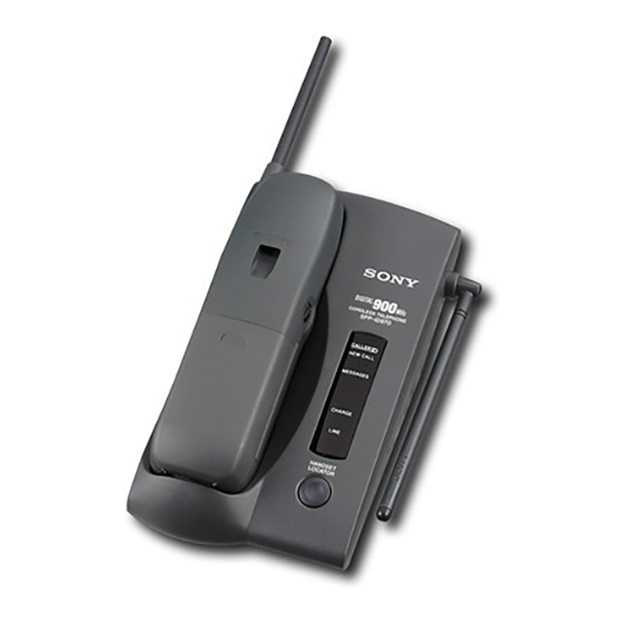
Photo: SPP-ID970
SPECIFICATIONS
Base unit
Power source
DC 9V from AC power adaptor
AC-T127
Battery charging time
Approx. 12 hours
Dimensions
Approx. 123 × 63 × 225 mm (w/h/d),
antenna excluded
× 2
(approx. 4
7/8
Antenna: Approx. 120 mm
(approx. 4
inches)
3/4
Mass
Approx. 360 g
(approx. 13 oz), wall bracket excluded
Design and specifications are subject to
change without notice.
Notes on Chip Component Replacement
• Never reuse a disconnected chip component.
• Notice that the minus side of a tantalum capacitor may be dam-
aged by heat.
– 1 –
US Model
Canadian Model
× 8
inches)
1/2
7/8
CORDLESS TELEPHONE
SPP-ID970
SPP-ID971
Advertisement
Table of Contents

Related Manuals for Sony SPP-ID970


Summary of Contents for Sony SPP-ID970
- Page 1 SPP-ID971 (9-927-617-81) With SUPPLEMENT-2 (9-927-617-82) Photo: SPP-ID970 SPECIFICATIONS General Base unit Frequency band (SPP-ID970) Power source 902 – 928 MHz DC 9V from AC power adaptor Frequency band (SPP-ID971) AC-T127 923.1 – 927.75 MHz Battery charging time Base unit : 18 µW Approx.
-
Page 2: Table Of Contents
Note for Replacement of the ASIC Board TABLE OF CONTENTS The ID is written in the ASIC board. When replacing the ASIC board, the U2001 on BASE MAIN board 1. GENERAL and U1001 on HAND MAIN board should be replaced together as Read This First ................ - Page 3 SECTION 1 GENERAL This section is extracted from SPP-ID970’s instruction manual. – 3 –...
- Page 4 – 4 –...
- Page 5 – 5 –...
- Page 6 – 6 –...
- Page 7 – 7 –...
- Page 8 – 8 –...
- Page 9 – 9 –...
- Page 10 – 10 –...
- Page 11 – 11 –...
-
Page 12: Disassembly
SECTION 2 DISASSEMBLY Note : This set can be disassemble according to the following sequence. HANDSET CASE (REAR) RF UNIT (HS), HAND MAIN BOARD BASE UNIT BASE (BOTTOM) BASE MAIN BOARD RF UNIT (BU) LED BOARD Note : Follow the disassembly procedure in the numerical order given. 2-1. -
Page 13: Base (Bottom)
2-3. BASE (BOTTOM) 2 BTP 3x12 6 base (bottom) 1 BTP 3x12 3 BTP 3x12 2-4. BASE MAIN BOARD 1 screws (3x30) 4 Removal the solders. 3 BTP 3x12 7 BASE MAIN board 2 BTP 3x12 5 Removal the solders. charge springs 6 Removal the solders. -
Page 14: Rf Unit (Bu)
2-5. RF UNIT (BU) 1 BTP 3x12 3 B 2x8 2 BTP 3x12 4 RF unit (BU) 2-6. LED BOARD 2 LED board 1 BTP 3x12 – 14 –... -
Page 15: Electrical Adjustments
SECTION 3 ELECTRICAL ADJUSTMENTS 3-1. HANDSET 1. Test Mode Entry— Press “PGM” key and enter “ TEST” on keypad. Alternative entry— Write 99h into LSB of location 9 in EEPROM. Exit— Press on “OFF” key. LCD test— Press the “7” key. Toggle TX power—... -
Page 16: Base Unit
3-2. BASE UNIT 1. Test Mode Entry— Simultaneously press the “HANDSET LOCATOR” key and toggle the “DIAL MODE” switch. When in test mode, the “LINE” and “CHARGE” LEDs will be light on. Alternative entry— Write 99h into LSB of location 9 in EEPROM. Exit—... -
Page 17: Diagrams
SPP-ID970/ID971 SECTION 4 DIAGRAMS 4-1. BLOCK DIAGRAM — BASE UNIT SECTION — ANT2001 TELESCOPIC ANTENNA RF UNIT (BU) SYSTEM CONTROL U2001 D1007-1009 T1001 HOOK DET U1002 RX AUDIO DSIN J1008 TXDATA TX DATA LINE PLL REF PLL REF RSSI APIN2... -
Page 18: Block Diagram -Handset Section
SPP-ID970/ID971 4-2. BLOCK DIAGRAM — HANDSET SECTION — ANT1001 HELICAL ANTENNA SYSTEM CONTROL U1001 RF UNIT (HS) PLL REF 64 PLL REF DSIN RX AUDIO U1005 TX DATA TXDATA SPEAKER RSSI ADIN2 PLL EN GPIO2/MON2 SER DATA OUT SER CLK... -
Page 19: Schematic Diagram -Base Unit Section (1/2)
SPP-ID970/ID971 4-3. SCHEMATIC DIAGRAM — BASE UNIT SECTION (1/2) — THIS NOTE IS COMMON FOR PRINTED WIRING BOARDS AND SCHEMATIC DIAGRAMS. (In addition to this, the necessary note is printed in each block.) For schematic diagrams • All capacitors are in µF unless otherwise noted. pF: µµF 50 WV or less are not indicated except for electrolytics and tantalums. -
Page 20: Schematic Diagram -Base Unit Section (2/2)
SPP-ID970/ID971 4-4. SCHEMATIC DIAGRAM — BASE UNIT SECTION (2/2) — • Refer to page 31 for IC Block Diagram. – 23 – – 24 –... -
Page 21: Printed Wiring Boards -Base Unit Section
SPP-ID970/ID971 4-5. PRINTED WIRING BOARDS — BASE UNIT SECTION — • Semiconductor Location Ref. No. Location (D1006) (D1007) (D1008) (D1009) (D1010) D1011 D1012 D1015 D1016 D2001 Q1006 (Q1007) Q1008 Q2001 Q2003 (U1001) (U1002) U1003 U2001 U2002 U2003 ) : SIDE B –... -
Page 22: Printed Wiring Board -Handset Section
SPP-ID970/ID971 4-6. PRINTED WIRING BOARD — HANDSET SECTION — • Semiconductor Location Ref. No. Location (D1001) (D1002) (D1003) (D1004) (D1006) D1008 D1010 D1016 D1018 (D1020) D1023 D1024 D1025 D1026 D1027 D1028 (D1030) (D1031) D1032 D1033 (Q1002) (Q1004) (Q1006) (Q1007) (Q1008) -
Page 23: Schematic Diagram -Handset Section
SPP-ID970/ID971 4-7. SCHEMATIC DIAGRAM — HANDSET SECTION — • Refer to page 31 for IC Block Diagram. – 29 – – 30 –... -
Page 24: Exploded Views
Ver 1.3 2000. 12 SECTION 5 EXPLODED VIEWS NOTE: • IC Block Diagram • The mechanical parts with no reference • -XX and -X mean standardized parts, so • Accessories and packing materials are number in the exploded views are not supplied. they may have some difference from the given in the last of this parts list. -
Page 25: Base Unit Section
Ver 1.3 2000. 12 5-2. BASE UNIT SECTION ANT2001 J1003, 1004 Ref. No. Part No. Description Remark Ref. No. Part No. Description Remark * 51 A-3672-868-A BASE MAIN BOARD, COMPLETE 3-038-086-01 BASE (TOP) (ID970) 7-685-548-19 SCREW +BTP 3X12 TYPE2 N-S 3-230-116-01 BASE (TOP) (ID971) 3-044-144-01 TERMINAL BOARD, ANTENNA 3-044-143-01 PLATE, ANTENNA RETAINER... -
Page 26: Electrical Parts List
SECTION 6 BASE MAIN ELECTRICAL PARTS LIST NOTE: • Due to standardization, replacements in • Items marked “*” are not stocked since The components identified by mark 0 or dotted line with mark the parts list may be different from the they are seldom required for routine service. - Page 27 BASE MAIN HAND MAIN Ref. No. Part No. Description Remark Ref. No. Part No. Description Remark Q1007 8-729-113-08 TRANSISTOR 2N3906 R2020 1-218-292-11 RES,CHIP 1/16W Q1008 8-729-026-06 TRANSISTOR MMBT3904LT1 R2021 1-216-821-11 METAL CHIP 1/16W Q2001 8-729-026-07 TRANSISTOR MMBT3906LT1 R2023 1-216-833-11 METAL CHIP 1/16W Q2003 8-729-050-67 TRANSISTOR SST297AT116...
- Page 28 HAND MAIN Ref. No. Part No. Description Remark Ref. No. Part No. Description Remark C1017 1-164-227-11 CERAMIC CHIP 0.022uF Q1006 8-729-026-07 TRANSISTOR MMBT3906LT1 C1018 1-162-918-11 CERAMIC CHIP 18PF Q1007 8-729-026-07 TRANSISTOR MMBT3906LT1 C1019 1-107-826-11 CERAMIC CHIP 0.1uF Q1008 T-941-615-31 TRANSISTOR MMBT3904LT1 C1020 1-135-201-11 TANTALUM CHIP 10uF Q1009...
- Page 29 HAND MAIN Ref. No. Part No. Description Remark < SWITCH > S1002 1-475-568-12 ENCODER, ROTARY S1003 1-771-833-11 SWITCH, SLIDE (VOL) < IC > U1001 X-3378-158-1 ASIC ASSY (ASIC BOARD, COMPLETE) U1002 1-505-594-11 BUZZER U1003 1-542-260-31 MICROPHONE, ELECTRET CONDENSER U1005 1-505-593-11 SPEAKER (2.8cm) U1006 8-759-466-52 IC CAT93C86S-LE10 U1007...
- Page 30 SPP-ID970/ID971 Sony Corporation 99K0414-1 9-927-617-11 Personal Audio Division Company Printed in Japan ©1999. 11 – 38 – Published by General Engineering Dept.
- Page 31 SPP-ID970/ID971 US Model SPP-ID970 Canadian Model SERVICE MANUAL SPP-ID971 Ver 1.1 2000. 07 SUPPLEMENT-1 File this supplement with the service manual. Subject : 1. Correction 2. Hand main board change (ECN-CPE00044, ECN-CPA00314) 1. Correction 1-1. ELECTRICAL PARTS LIST The ASIC MOUNT and EEPROM have two versions. In service, check the version before replacing parts.
- Page 32 1-2. ELECTRICAL ADJUSTMENTS 1) Frequency Tables This section outlines the RF frequencies and corresponding channel numbers. The handset uses a high side LO while the base uses a low side LO to down-convert the incoming signal. 1. Handset Frequencies (Unit : MHz) 2.
- Page 33 2) HANDSET 3) BASE UNIT 1. Test Mode 1. Test Mode Entry— Press “PGM” key and enter “ TEST” on keypad. Entry— Simultaneously press the “HANDSET LOCATOR” key and toggle the “DIAL MODE” switch. When in test mode, the “LINE” and Alternative entry—...
- Page 34 SPP-ID970/ID971 2. Hand Main Board Change 2-1. PRINTED WIRING BOARD — HANDSET SECTION — S1003 HAND MAIN BOARD (SIDE A) J1010 LCD1001 S1013 S1016 LCD MODULE S1019 S1010 S1007 S1004 D1023 3/DEF 6/MNO FLASH 9/WXYZ REDIAL D1027 ANT1001 HELICAL ANTENNA...
- Page 35 SPP-ID970/ID971 2-2. SCHEMATIC DIAGRAM — HANDSET SECTION — For schematic diagrams • All capacitors are in µF unless otherwise noted. pF: µµF • Voltage is dc with respect to ground under no-signal 50 WV or less are not indicated except for electrolytics condition.
- Page 36 SPP-ID970/ID971 HAND MAIN HAND MAIN Ref. No. Part No. Description Remark 2-3. ELECTRICAL PARTS LIST R1022 1-216-231-00 RES,CHIP 1/8W NOTE: R1025 1-219-614-11 METAL CHIP 301K 0.50% 1/16W • Due to standardization, replacements in • Items marked “*” are not stocked since...
- Page 37 SPP-ID970/ID971 THIS NOTE IS COMMON FOR PRINTED WIRING BOARDS AND SCHEMATIC DIAGRAMS. (In addition to this, the necessary note is printed in each block.) US Model For schematic diagrams SPP-ID970 • All capacitors are in µF unless otherwise noted. pF: µµF...
- Page 38 SPP-ID970/ID971 1. PRINTED WIRING BOARD — BASE UNIT SECTION — • Refer to page 2 for Note. • Semiconductor Location BASE MAIN BOARD (SIDE A) Ref. No. Location Ref. No. Location (D1006) (Q1007) G-13 (D1007) Q1008 (D1008) Q2001 R2023 C2001...
- Page 39 SPP-ID970/ID971 BASE MAIN BOARD (SIDE B) S2001 ANT2001 DIAL MODE TELESCOPIC ANTENNA J2003 C2011 C2019 C2023 TX PWR J2012 RF UNIT (BU) X2001 LED BOARD RX AUDIO C2024 ATE RX ATE TX DSP PWR PX PWR C2004 C2039 L1005 L1001...
- Page 40 SPP-ID970/ID971 2-1. SCHEMATIC DIAGRAM — BASE UNIT SECTION (1/2) — • Refer to page 2 for Note. – 7 – – 8 –...
- Page 41 SPP-ID970/ID971 2-2. SCHEMATIC DIAGRAM — BASE UNIT SECTION (2/2) — • Refer to page 2 for Note. – 9 – – 10 –...
- Page 42 SPP-ID970/ID971 BASE MAIN BASE MAIN Ref. No. Part No. Description Remark Ref. No. Part No. Description Remark 3. ELECTRICAL PARTS LIST < TRANSISTOR > R2009 1-216-823-11 METAL CHIP 1.5K 1/16W NOTE: R2010 1-216-833-11 METAL CHIP 1/16W • Due to standardization, replacements in •...