Table of Contents
Advertisement
Quick Links
QQ
3 7 63 1515 0
SERVICE MANUAL
Ver 1.2 2003. 08
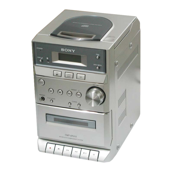
HCD-EP315 is the Amplifier, CD player, Tape
Deck and Tuner section in CMT-EP315.
TE
L 13942296513
Amplifier section
DIN power output (rated): 7 + 7 W
Continuous RMS power output (reference):
Music power output (reference):
Inputs
MD IN (phono jacks):
Outputs
PHONES (stereo minijack):
SPEAKER:
CD player section
System
Laser
Frequency response
www
.
Sony Corporation
9-877-443-03
2003H16-1
Home Audio Company
© 2003.08
Published by Sony Engineering Corporation
http://www.xiaoyu163.com
Tape deck section
Recording system
Frequency response
(6 ohms at 1 kHz, DIN)
10 + 10 W
(6 ohms at 1 kHz, 10%
Tuner section
THD)
FM stereo, FM/AM superheterodyne tuner
20 + 20 W
FM tuner section
Tuning range
Sensitivity 500 mV,
Antenna
impedance 47 kilohms
Antenna terminals
Intermediate frequency
AM tuner section
Accepts headphones with
Tuning range
an impedance of 8 ohms or
more
Accepts impedance of 6 to
Antenna
16 ohms.
Intermediate frequency
Compact disc and digital
audio system
Semiconductor laser
λ
(
=780 nm)
Emission duration:
continuous
2 Hz – 20 kHz (±0.5 dB)
x
ao
y
i
http://www.xiaoyu163.com
HCD-EP315
8
Model Name Using Similar Mechanism
CD Mechanism Type
CD
Section
Base Unit Name
Optical Pick-up Name
Model Name Using Similar Mechanism
TAPE
Q Q
Section
Tape Transport Mechanism Type
3
6 7
1 3
SPECIFICATIONS
4-track 2-channel stereo
50 – 13,000 Hz (±3 dB),
using Sony TYPE I
cassettes
87.5 – 108.0 MHz (50-kHz
step)
FM lead antenna
75 ohms balanced
10.7 MHz
531 – 1,602 kHz
(with the tuning interval
set at 9 kHz)
AM loop antenna, external
antenna terminal
450 kHz
MICRO HI-FI COMPONENT SYSTEM
u163
.
2 9
9 4
2 8
AEP Model
HCD-EP313
KSM-213EDP
BU-K7BD44B
KSS-213E/C2N
HCD-EP313
ADR2080FR4
1 5
0 5
8
2 9
9 4
General
Power requirements
Power consumption
Dimensions (w/h/d)
Mass
Supplied accessories
Design and specifications are subject to change
without notice.
m
co
9 9
2 8
9 9
230 V AC, 50/60 Hz
32 watts
0.3 watts (in the standby
mode)
Approx. 148 × 233 × 208
mm
Approx. 2.9 kg
Remote (1)
R6 (size AA) batteries (2)
AM loop antenna (1)
FM lead antenna (1)
Advertisement
Table of Contents

Related Manuals for Sony HCD-EP315


Summary of Contents for Sony HCD-EP315
- Page 1 HCD-EP315 3 7 63 1515 0 SERVICE MANUAL AEP Model Ver 1.2 2003. 08 HCD-EP315 is the Amplifier, CD player, Tape Deck and Tuner section in CMT-EP315. Model Name Using Similar Mechanism HCD-EP313 CD Mechanism Type KSM-213EDP Section Base Unit Name...
-
Page 2: Table Of Contents
COMPONENTS IDENTIFIED BY MARK 0 OR DOTTED LINE WITH MARK 0 ON THE SCHEMATIC DIAGRAMS AND IN THE PARTS LIST ARE CRITICAL TO SAFE OPERATION. REPLACE THESE COMPONENTS WITH SONY PARTS WHOSE PART NUMBERS APPEAR AS SHOWN IN THIS MANUAL OR IN SUPPLEMENTS PUBLISHED BY SONY. -
Page 3: Servicing Notes
HCD-EP315 SECTION 1 SERVICING NOTES 3 7 63 1515 0 Notes on chip component replacement CAUTION • Never reuse a disconnected chip component. Use of controls or adjustments or performance of procedures • Notice that the minus side of a tantalum capacitor may be dam- other than those specified herein may result in hazardous aged by heat. - Page 4 HCD-EP315 3 7 63 1515 0 Service Position of the CD Mechanism Deck CD mechanism deck (KSM-213EDP) L 13942296513 Service Position of the Tape Cassette Mechanism Deck u163 Tape cassette mechanism deck (ADR2080FR4) http://www.xiaoyu163.com...
-
Page 5: General
HCD-EP315 SECTION 2 GENERAL 3 7 63 1515 0 This section is extracted from instruction manual. List of button locations and reference pages How to use this page Illustration number Use this page to find the location of buttons and other... -
Page 6: Setting The Clock
HCD-EP315 3 7 63 1515 0 Remote control ALPHABETICAL ORDER BUTTON DESCRIPTIONS ?/1 (power) 1 (5, 9, 13) A – M P – Z m/M (fast forward/rewind) BASS +/– 0 (12) PLAY MODE/DIRECTION qd 6 (6) (6, 7) CLEAR 8 (8, 9) ./>... -
Page 7: Disassembly
HCD-EP315 SECTION 3 DISASSEMBLY 3 7 63 1515 0 • This set can be disassembled in the order shown below. REAR CABINET CD CABINET SECTION CD MECHANISM DECK (KSM-213EDP) OPTICAL PICK-UP FRONT PANEL SECTION (KSS-213E/C2N) CONTROL BOARD, TAPE MECHANISM DECK... -
Page 8: Cd Cabinet Section
HCD-EP315 3 7 63 1515 0 3-2. CD Cabinet Section 7 CD cabinet section 6 connector 2p (CN101) 1 screw (+BVTP 3 × 8) 4 two claws 2 w ire (flat type) 21p (CN101) 3 two claws L 13942296513 3-3. -
Page 9: Control Board, Back Light Board
HCD-EP315 3 7 63 1515 0 3-4. CONTROL Board, BACK LIGHT Board 3 nine screws (+BVTP 3 × 8) 5 CONTROL board 4 w ire (flat type) 21p (CN301) 8 BACK LIGHT board 2 screw 1 volume knob 6 two claws (+BVTP 3 ×... -
Page 10: Cassette Door Assy
HCD-EP315 3 7 63 1515 0 3-6. Cassette Door Assy 2 cassette door assy 1 two claws 3-7. MAIN Board, POWER Board L 13942296513 2 screw 3 MAIN board 5 four screws (+BVTP 3 × 8) (+BVTP 4 × 12) -
Page 11: Cd Mechanism Deck (Ksm-213Edp)
HCD-EP315 3 7 63 1515 0 3-8. CD Mechanism Deck (KSM-213EDP) 5 panel CD 4 three claws 3 two screws (+PWH 2.6 × 10) 6 two cushion rubbers q; w ire (flat type) 16p (CN102) qs CD mechanism deck... -
Page 12: Mechanical Adjustments
HCD-EP315 SECTION 4 MECHANICAL ADJUSTMENTS 3 7 63 1515 0 Precaution Clean the following parts with a denatured alcohol-moistened swab: record/playback heads pinch rollers erase head rubber belts capstan idlers Demagnetize the record/playback head with a head demag- netizer. -
Page 13: Electrical Adjustments
HCD-EP315 SECTION 5 ELECTRICAL ADJUSTMENTS 3 7 63 1515 0 Mode: Playback DECK SECTION 0 dB=0.775V test tape Demagnetize the record/playback head with a head demagnetizer. P-4-A100 MAIN board J203 (10kHz, –10dB) Do not use a magnetized screwdriver for the adjustments. - Page 14 HCD-EP315 3 7 63 1515 0 RFDC signal waveform CD SECTION VOLT/DIV: 200 mV TIME/DIV: 500 ns Note: 1. CD Block is basically designed to operate without adjustment. There- fore, check each item in order given. 2. Use YEDS-18 disc (3-702-101-01) unless otherwise indicated.
- Page 15 HCD-EP315 3 7 6 3 1 5 1 5 0 E-F Balance Check Checking Location: Connection: – CD BOARD (Conductor Side) – oscilloscope CD board TP (TE) TP (DVC) – Procedure: Connect an oscilloscpe to test point TP (TE) and TP (DVC) on TP (VC) the CD board.
-
Page 16: Diagrams
HCD-EP315 SECTION 6 DIAGRAMS 3 7 6 3 1 5 1 5 0 • Circuit Boards Location • Waveforms – CD Board – – CONTROL Board – – MAIN Board – MAIN board IC103 qg (RFAC) IC301 0 8.6MHz OUT... -
Page 17: Block Diagram
HCD-EP315 6-1. Block Diagram 3 7 6 3 1 5 1 5 0 PB/REC EQ AMP J201 IC601 R CH IC800 J202 AUX L OUT L PHONES SYSTEM CONTROLLER TU L OUT R R-CH IC301 MUTE R-CH TAPE L... -
Page 18: Printed Wiring Board - Cd Section
HCD-EP315 6-2. Printed Wiring Board – CD Section – • See page 16 for Circuit Boards Location. 3 7 6 3 1 5 1 5 0 • Semiconductor Location Ref. No. Location KSS-213E/C2N D101 IC101 IC102 IC103 M102 Q101... -
Page 19: Schematic Diagram - Cd Section
HCD-EP315 6-3. Schematic Diagram – CD Section – • See page 16 for Waveforms. • See page 28 for IC Block Diagrams. 3 7 6 3 1 5 1 5 0 TP(VC) C150 KSS-213E/C2N (RF) 1 3 9 4 2 2 9 6 5 1 3... -
Page 20: (Component Side)
HCD-EP315 6-4. Printed Wiring Board – MAIN Section (COMPONENT SIDE) – • See page 16 for Circuit Boards Location. 3 7 6 3 1 5 1 5 0 ANTENNA (TO TUNER UNIT) • Semiconductor Location MAIN BOARD Ref. No. Location... -
Page 21: (Conductor Side)
HCD-EP315 6-5. Printed Wiring Board – MAIN Section (CONDUCTOR SIDE) – • See page 16 for Circuit Boards Location. 3 7 6 3 1 5 1 5 0 • Semiconductor Location MAIN BOARD Ref. No. Location (CONDUCTOR SIDE) IC601... -
Page 22: Schematic Diagram - Main Section
HCD-EP315 6-6. Schematic Diagram – MAIN Section – • See page 16 for Waveform. • See page 29 for IC Block Diagram. 3 7 6 3 1 5 1 5 0 (TO TUNER UNIT) MAIN BOARD ANTENNA (CD DOOR) -
Page 23: (Component Side)
HCD-EP315 6-7. Printed Wiring Board – CONTROL Section (COMPONENT SIDE) – • See page 16 for Circuit Boards Location. 3 7 6 3 1 5 1 5 0 • Semiconductor Location Ref. No. Location CONTROL BOARD (COMPONENT SIDE) D301... -
Page 24: (Conductor Side)
HCD-EP315 6-8. Printed Wiring Board – CONTROL Section (CONDUCTOR SIDE) – • See page 16 for Circuit Boards Location. 3 7 6 3 1 5 1 5 0 • Semiconductor Location Ref. No. Location CONTROL BOARD (CONDUCTOR SIDE) IC301... -
Page 25: Schematic Diagram - Control Section
HCD-EP315 6-9. Schematic Diagram – CONTROL Section – • See page 16 for Waveforms. 3 7 6 3 1 5 1 5 0 CONTROL BOARD BACK LIGHT BOARD BACK LIGHT IC303 LIQUID SWITCH CRYSTAL REMOTE DISPLAY SENSOR SWITCH (STANDBY) -
Page 26: Printed Wiring Board - Power Section
HCD-EP315 6-10. Printed Wiring Board – POWER Section – • See page 16 for Circuit Boards Location. 3 7 6 3 1 5 1 5 0 • Semiconductor Location Ref. No. Location D901 TRANSFORMER BOARD D902 D903 D904 TO MAIN... -
Page 27: Schematic Diagram - Power Section
HCD-EP315 6-11. Schematic Diagram – POWER Section – 3 7 6 3 1 5 1 5 0 TRANSFORMER BOARD : N O T R E P L A C E A B L E B U I LT I N T R A N F O R M E R... - Page 28 HCD-EP315 3 7 6 3 1 5 1 5 0 • IC Block Diagrams – CD Board – IC101 CXD3017Q IC103 CXA2581N-T4 RW/ROM DC OFST RFDCI – ERROR – DIGITAL CORRECTOR RFDCO DIGITAL ASYMMETRY CORRECTOR OPERATIONAL LRCK AMPLIFIER ANALOG SWITCH...
- Page 29 HCD-EP315 3 7 63 1515 0 – MAIN Board – IC601 BD3881FV L 13942296513 IC204 LA4636 OUTPUT OUTPUT + – – INPUT INPUT 1 2 3 u163 http://www.xiaoyu163.com...
-
Page 30: Ic Pin Function Description
HCD-EP315 3 7 63 1515 0 6-12. IC Pin Function Description • IC301 LC877140A (SYSTEM CONTROLLER) Pin No. Pin Name Description O-CLOCK Clock output to the CD unit I-SQSO SUB-Q data input from the CD unit O-PWM1 PWM1 signal output to the CD unit... - Page 31 HCD-EP315 3 7 63 1515 0 Pin No. Pin Name Description O-XLAT Latch signal output to the CD unit O-CDON CD power supply control signal output O-SQCK SUBQ clock output to the CD unit I-SENS SENS signal input from the CD unit...
-
Page 32: Overall Section
HCD-EP315 Ver 1.2 2003. 08 SECTION 7 EXPLODED VIEWS 3 7 63 1515 0 NOTE: • -XX, -X mean standardized parts, so they may • The mechanical parts with no reference number The components identified by mark 0 or have some differences from the original one. -
Page 33: Front Panel Section
HCD-EP315 Ver 1.2 2003. 08 3 7 63 1515 0 7-2. Front Panel Section supplied supplied supplied L 13942296513 supplied Ref. No. Part No. Description Remark Ref. No. Part No. Description Remark A-4740-923-A DOOR CASSETTE ASSY 4-245-248-01 BUTTON,CD 4-245-244-01 HOLDER,CASSETTE... -
Page 34: Cd Cabinet Section
HCD-EP315 Ver 1.2 2003. 08 3 7 63 1515 0 7-3. CD Cabinet Section not supplied S800 not supplied not supplied L 13942296513 not supplied not supplied not supplied KSM-213EDP not supplied Ref. No. Part No. Description Remarks Ref. No. -
Page 35: Optical Pick-Up Block (Ksm-213Edp)
HCD-EP315 Ver 1.1 2003. 07 3 7 63 1515 0 7-4. Optical Pick-up Block (KSM-213EDP) L 13942296513 Ref. No. Part No. Description Remarks 0 604 8-820-221-01 OPTICAL PICK-UP KSM-213EDP u163 The components identified by mark 0 or dotted line with mark 0 are critical for safety. -
Page 36: Electrical Parts List
HCD-EP315 SECTION 8 BACK LIGHT ELECTRICAL PARTS LIST 3 7 63 1515 0 NOTE: • Due to standardization, replacements in the • CAPACITORS: • SEMICONDUCTORS parts list may be different from the parts uF: µF In each case, u: µ, for example: specified in the diagrams or the components •... - Page 37 HCD-EP315 CONTROL 3 7 63 1515 0 Ref. No. Part No. Description Remarks Ref. No. Part No. Description Remarks < RESISTOR > A-4732-942-A CONTROL BOARD, COMPLETE ************************ R101 1-216-821-11 METAL CHIP 1/16W R102 1-216-845-11 METAL CHIP 100K 1/16W 4-245-258-01 HOLDER,LED...
- Page 38 HCD-EP315 CONTROL 3 7 63 1515 0 Ref. No. Part No. Description Remarks Ref. No. Part No. Description Remarks < FERRITE BEAD > R307 1-216-809-11 METAL CHIP 1/16W R308 1-216-821-11 METAL CHIP 1/16W FB301 1-400-297-11 INDUCTOR R309 1-216-821-11 METAL CHIP...
- Page 39 HCD-EP315 CONTROL MAIN 3 7 63 1515 0 Ref. No. Part No. Description Remarks Ref. No. Part No. Description Remarks R366 1-247-887-00 CARBON 220K 1/4W C223 1-126-962-11 ELECT 3.3uF 20.00% 50V R367 1-216-841-11 METAL CHIP 1/16W C224 1-126-961-11 ELECT 2.2uF...
- Page 40 HCD-EP315 MAIN 3 7 63 1515 0 Ref. No. Part No. Description Remarks Ref. No. Part No. Description Remarks C650 1-164-218-11 CERAMIC CHIP 180PF 0.25PF 50V D404 8-719-991-33 DIODE 1SS133T-72 C651 1-126-961-11 ELECT 2.2uF 20.00% 50V D405 8-719-109-89 DIODE MTZJ-T-72-5.6B...
- Page 41 HCD-EP315 MAIN 3 7 63 1515 0 Ref. No. Part No. Description Remarks Ref. No. Part No. Description Remarks Q502 6-550-296-01 TRANSISTOR 2SA1980G R441 1-216-817-11 METAL CHIP 1/16W Q504 8-729-901-05 TRANSISTOR DTA124EK R442 1-249-425-11 CARBON 4.7K 1/4W F Q505...
- Page 42 HCD-EP315 Ver 1.1 2003. 07 MAIN TRANSFORMER 3 7 63 1515 0 Ref. No. Part No. Description Remarks Ref. No. Part No. Description Remarks R655 1-216-836-11 METAL CHIP 1/16W < COIL > R656 1-216-836-11 METAL CHIP 1/16W R657 1-216-852-11 METAL CHIP...
- Page 43 HCD-EP315 3 7 63 1515 0 MEMO L 13942296513 u163 http://www.xiaoyu163.com...
- Page 44 HCD-EP315 3 7 63 1515 0 REVISION HISTORY Clicking the version allows you to jump to the revised page. Also, clicking the version at the upper right on the revised page allows you to jump to the next revised page.