Table of Contents
Advertisement
SERVICE MANUAL
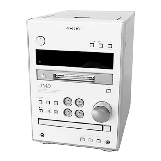
HCD-J3MD is the amplifir, CD, MD, TAPE deck
and tuner section in CMT-J3MD.
HCD-J3MD
Model Name Using Similar Mechanism HCD-MD373
Mechanism Type
CD
SECTION
Base Unit Type
Optical Pick-up Type
Model Name Using Similar Mechanism HCD-MD373
MD
Mechanism Type
SECTION
Optical Pick-up Type
Model Name Using Similar Mechanism NEW
CASSETTE
SECTION
Tape Transport Mechanism Type
SPECIFICATIONS
COMPACT COMPONENT Hi-Fi SYSTEM
AEP Model
UK Model
E Model
Chinese Model
CDM55A-5SBD32
BU-5SBD32
KSS-213BA/F-NP
MDM-5H
KMS-260B/J1N
CMAL1Z027A
— Continued on next page —
Advertisement
Table of Contents

Related Manuals for Sony HCD-J3MD


Summary of Contents for Sony HCD-J3MD
- Page 1 HCD-J3MD SERVICE MANUAL AEP Model UK Model E Model Chinese Model HCD-J3MD is the amplifir, CD, MD, TAPE deck and tuner section in CMT-J3MD. Model Name Using Similar Mechanism HCD-MD373 Mechanism Type CDM55A-5SBD32 SECTION Base Unit Type BU-5SBD32 Optical Pick-up Type...
-
Page 2: Press The Lm/I/Cd/Tuning – Button Or Ml/Tuning + Button And When "[Service]" Is Displayed, Press The Enter
SELF-DIAGNOSIS FUNCTION The self-diagnosis function consists of error codes for customers which are displayed automatically when errors occur, and error codes which show the error history in the test mode during servicing. For details on how to view error codes for the customer, refer to the following box in the instruction manual. - Page 3 ITEMS OF ERROR HISTORY MODE ITEMS AND CONTENTS Selecting the Test Mode Display Details of History Displays the recording time. total rec Displayed as “rππππππh”. The displayed time is the total time the laser is set to the high power state. This is about 1/4 of the actual recording time.
- Page 4 COMPONENTS IDENTIFIED BY MARK ! OR DOTTED LINE WITH MARK ! ON THE SCHEMATIC DIAGRAMS AND IN THE PARTS LIST ARE CRITICAL TO SAFE OPERATION. REPLACE THESE COMPONENTS WITH SONY PARTS WHOSE PART NUMBERS APPEAR AS SHOWN IN THIS MANUAL OR IN SUPPLEMENTS PUBLISHED BY SONY.
-
Page 5: Table Of Contents
CRITIQUES POUR LA SÉCURITÉ DE FONCTIONNEMENT. NE COMPONENTS WITH SONY PARTS WHOSE PART NUMBERS REMPLACER CES COMPOSANTS QUE PAR DES PIÈSES SONY APPEAR AS SHOWN IN THIS MANUAL OR IN SUPPLEMENTS DONT LES NUMÉROS SONT DONNÉS DANS CE MANUEL OU PUBLISHED BY SONY. -
Page 6: Servicing Note
SECTION 1 SERVICING NOTE Note 1: “R” As this unit has only a few buttons, some operations require the use of remote commander (provided with RM-SJ373/unit: 1-418-554-11) buttons. These operations are indicated as “R” in this manual. Example: MENU/NO “R” ...Press the MENU/NO button of the remote commander. DRAWING OUT THE TRAY DURING POWER OUT CLEANING THE OPTIAL PICKUP (CD PLAYER) Floating screw... - Page 7 SERVICE POSITION OF THE CASSETTE MECHANISM DECK Cassette mechanism deck SERVICE POSITION OF THE POWER BOARD Back panel Remove the TRANS board together with back panel (referring to [MAIN Board] ) and move it in the direction of the arrow. TRANS board Heat sink AMP board...
- Page 8 CD Text Display • This unit displays CD text. Text is displayed for the first 50 track only and will not be displayed from the 51st track onwards. Do not suspect a fault in this case. In some cases, some special characters will not be displayed and may be replaced by other characters. D onot suspect a fault in this case. Cold Reset •...
- Page 9 LED and Fluorescent Indicator Tube All Lit, Key Check Mode Procedure : When the power ON, press the ?/1 button while pressing PLAY MODE/DIRECTION/TUNIG MODE button and s button together. Frame of the MD mark and the CD mark flash, and “BASS/TRE FLAT” appears for a moment. When the VOLUME knob is turned clockwise, “VOLUME MAX”...
- Page 10 Aging Mode • Mode for repeating operations of the CD player and TC deck automatically. When errors occur: Aging stops and a message indicating that an error has occurred such as “CD MEC ERR” is displayed. (For details of errors, refer to “Error History Display Mode”.) When no errors occur: Aging is repeatedly performed.
- Page 11 • Reading the Mechanism Error History Display (To switch the history, press the PLAY MODE/DIRECTION/TUNING MODE button.) Display E@@M**#*$* @@: Error number. 00 is the latest *: Invalid #: Load in operations related D: Operations stopped due to problems other than mechanism related during CLOSE E: Operations stopped due to problems other than mechanism related during OPEN C: Operations stopped due to problems other than mechanism related during chucking up $: Load out operations related...
- Page 12 JIG FOR CHECKING BD (MD) BOARD WAVEFORM The special jig (J-2501-149-A) is useful for checking the waveform of the BD (MD) board. The names of terminals and the checking items to be performed are shown as follows. GND : Ground I+3V : For measuring IOP (Check the deterioration of the optical pick-up laser) IOP : For measuring IOP (Check the deterioration of the optical pick-up laser) TEO : TRK error signal (Traverse adjustment)
- Page 13 IOP Data Recording and Display When optical Pick-up and Non-volatile Memory (IC171 of BD (MD)board) are Replaced The IOP value labeled on the optical pick-up can be recorded in the non-volatile memory. By recording the value, it will eliminate the need to look at the value on the label of the optical pick-up.
- Page 14 Checks Prior to Parts Replacement and Adjustments Before performing repairs, perform the following checks to determine the faulty locations up to a certain extent. Details of the procedures are described in “5 Electrical Adjustments”. Criteria for Determination Measure if unsatisfactory: (Unsatisfactory if specified value is not satisfied) Laser power check •...
- Page 15 Forced Reset The system microprocessor can be reset in the following procedure. Use these procedure when the unit cannot be operated normally due to hung-up of the microprocessor, etc. Use of the RESET switch is recommended when the machine cannot exit the REtry CASE DISPLAY mode or a machine does not operate correctly after re-assembling.
- Page 16 Retry Cause Display Mode • In this test mode, the causes for retry of the unit during recording can be displayed on the fluorescent indicator tube. During playback, the “track mode” for obtaining track information will be set. This is useful for locating the faulty part of the unit. •...
- Page 17 Reading the Track Mode Display Higher Bits Lower Bits Hexa- Details Hexadecimal decimal b7 b6 b5 b4 b3 b2 b1 b0 When 0 When 1 Binary Emphasis ON Emphasis OFF Monaural Stereo This is 2-bit display. Normally 01. 01:Normal audio. Others:Invalid Audio (Normal) Invalid Digital copy...
-
Page 18: General
SECTION 2 GENERAL Identifying the Parts Front Panel qf qg 1 ?/1 Power switch 0 Recording button 2 MD slot SYNCHRO REC button 3 MD A (eject) button t CD-MD t CD-TAPE t TAPE-MD 4 Disk tray DUAL T MD-TAPE T 5 CD A (eject) button 6 VOLUME knob ENTER/START button... - Page 19 This section is extracted from instruction manual. Rear Panel 1 Reset switch 2 Speaker terminal 3 AM antenna termianal 4 FM antenna terminal 5 Power cord...
-
Page 21: Disassembly
SECTION 3 DISASSEMBLY Note : Follow the disassembly procedure in the numerical order given. 3-1. UPPER COVER q; Two screws 9 Three screws (+ BVTP 3 × 10) 3 Two screws (+ BVTP 3 × 10) qa Upper cover (Remove in the direction 1 Screw of the arrow.) (Case 3 TP 2) -
Page 22: Panel Board
3-3. PANEL BOARD 3 Two screws (+ BVTP 3 × 10) 9 Holder (MD) 5 Screw qa Five screws (+ BVTP 2.6 × 8) (+ BVTP 2.6 × 8) qg Flat cable (35 core) 2 Screw (+ BVTP 3 × 10) 6 Screw (+ BVTP 2.6 ×... -
Page 23: Cassette Machanism
3-5. CASSETTE MACHANISM q; Screw qa Screw (+ BVTP 3 × 10) (+ BVTP 3 × 10) qd Two screws qs Cassette mechanism deck qh FR/Belt qg Belt main 4 Flat cable (12 core) qf Motor 7 Two craws 6 Two crews 9 Connector (6P) 8 TC board 5 Flat cable (25 core) -
Page 24: Cd Mechanism Deck
3-7. CD MECHANISM DECK 1 Screw (+ BVTT 3 × 6) 4 CD mechanism deck (Two claws) 3 Connector (6P) 2 Flat cable (25 core) 3-8. TRAY, GEAR AND CAM 4 Belt (CDM55) 5 Bushing 6 Pulley (LDG) 8 Gear (B) 9 Gear (A) 7 Roller 0 Cam (CDM55) -
Page 25: Bd (Cd) Board, Spindle Motor (M101) And Sled Motor (M102)
3-9. CD BASE UNIT 3-10. OPTICAL PICK-UP SECTION OF CD (KSS-213BA/F-NP) 3 Optical pick-up (for CD) 1 Floating screw 2 Remove the Holder (BU) assembly (PTPWH M2.6) in the direction of arrow A. 1 Release the lever in the arrow direction B. 4 Flat type wire (16 core) 2 Sled shaft... -
Page 26: Md Mechanism Deck
3-12. MD MECHANISM DECK 1 Two Step screws 2 Two Step screws (BVTPWH M3) (BVTPWH M3) 3 MD mechanism deck 4 Connector (7P) 5 Flat type wire (21 core) 6 Flat type wire (23 core) 7 Bracket (MDM) 3-13. SLIDER (CAM) 6 Slider (CAM) •... -
Page 27: Base Unit (Mbu-5A) And Bd (Md) Board
3-14. BASE UNIT (MBU-5A) and BD (MD) BOARD 2 Base unit (MBU-5A) 6 Flexible board 7 Flexible board 1 Three screws (BTP 2.6x6) Spindle motor CN104 3 Remove the two solders. Sled motor Read wire's color CN110 Red : + CN101 Black : - 4 Remove the two solders. -
Page 28: Spindle Motor (M901) And Sled Motor (M902) (Md)
3-17. SPINDLE MOTOR (M901) and SLED MOTOR (M902) (MD) 4 Three screws (B 2x5) 3 Gear (SL-B) 1 Screw (M1.7) 2 Gear (SL-A) 5 Spindle motor (M901) The BD (MD) board is soldered at two parts. (See page 24.) 6 Two screws (P 1.7x2.5) 7 Sled motor (M902) -
Page 29: When The Power On, Press The ?/1 Button While Pressing The S Button And Z Tape Button Together
SECTION 4 TEST MODE Note 1: About “R” As this unit has only a few buttons, some operations require the use of remote commander (RM-SJ373/provided with unit: 1-418-554-11) buttons. These operations are indicated as “R” in this manual. Example: MENU/NO “R” ...Press the MENU/NO button of the remote commander. 4-1. - Page 30 4-5. SELECTING THE TEST MODE There are 31 types of test modes as shown below. The groups can be switched by pressing the lm/TUNING – button or ML/ TUNING + button. After selecting the group to be used, press the ENTER/YES “R” button. After setting a certain group, pressing the lm/TUNING –...
- Page 31 4-5-1. Operating the Continuous Playback Mode Entering the continuous playback mode 1 Set the disc in the unit. (Whichever recordable discs or discs for playback only are available.) 2 Press the lm/TUNING – button or ML/TUNING + button and display “CPLAY MODE”. 3 Press the ENTER/YES “R”...
- Page 32 4-6. FUNCTIONS OF OTHER BUTTONS Function Contents Sets continuous playback when pressed in the STOP state. When pressed during continuous playback, the tracking servo turns ON/OFF. Stops continuous playback and continuous recording. ML/TUNING + The sled moves to the outer circumference only when this is pressed. lm/TUNING –...
- Page 33 MEANINGS OF OTHER DISPLAYS Contents Display When Lit When Off During continuous playback (CLV: ON) (green)* STOP (CLV: OFF) Tracking servo OFF (orange)* Tracking servo ON Recording mode ON Recording mode OFF CLV low speed mode SYNC CLV normal mode ABCD adjustment completed LEVEL-SYNC Tracking offset cancel ON...
-
Page 34: Electrical Adjustments
SECTION 5 ELECTRICAL ADJUSTMENTS MD SECTION 5-1. Parts Replacement and Adjustment • Check and adjust the MDM and MBU as follows. The procedure changes according to the part replaced • Abbreviation : Optical pick-up OWH: Overwrite head • Temperature compensation offset check •... - Page 35 5-2. PRECAUTIONS FOR CHECKING LASER DIODE Perform the adjustments to be needed in the order shown. Use the following tools and measuring devices. EMISSION • Check Disc (MD) TDYS-1 To check the emission of the laser diode during adjustments, never (Parts No.
- Page 36 5-6. Checks Prior to Repairs Press the MENU/NO “R” button and display “LDPWR CHECK” and stop the laser emission. These checks are performed before replacing parts according to (The MENU/NO “R” button is effective at all times to stop the “approximate specifications”...
- Page 37 9. Press the ENTER/YES “R” button and display “EFB = 5-6-4. Focus Bias Check MO-P”.Then, the optical pick-up moves to the pit area Change the focus bias and check the focus tolerance amount. automatically and servo is locked. Checking Procedure : 10.
- Page 38 8. “C1 = AD = ” will be displayed. Display Procedure : 9. Check that the C1 error becomes 50 or less and the AD error 2 1. Press the lm/TUNING – button or ML/TUNING + or less. button to display “Iop Read”. 10.
- Page 39 5-11. TRAVERSE ADJUSTMENT 3. Press the ENTER/YES “R” button once and display “LD 0.9 mW $ ”. Connection : 4. Press the lm/TUNING – button or ML/TUNING + Oscilloscope button so that the reading of the laser power meter becomes 0.85 to 0.91 mW.
- Page 40 9. Press the ENTER/YES “R” button, and save the adjustment 5-12. FOCUS BIAS ADJUSTMENT results in the non-volatile memory. (“EFB = SAVE” will be Adjusting Procedure : displayed for a moment.) 1. Load a test disk (MDW-74/AU-1). 10. “EFB = MO-P”...
- Page 41 5-13. ERROR RATE CHECK 5-15. Auto Gain Control Output Level 5-13-1. CD Error Rate Check Adjustment Checking Procedure : Be sure to perform this adjustment when the pickup is replaced. 1. Load a check disc (MD) TDYS-1. If the adjustment results becomes “Adjust NG!”, the pickup may be 2.
- Page 42 CD SECTION 6. After check, remove the lead wire connected in step 2. Note: Clear RF signal waveform means that the shape “◊” can be Note: clearly distinguished at the center of the waveform. CD Block is basically constructed to operate without adjustment.
- Page 43 CASETTE SECTION 0 dB=0.775V 3. Phase check Model: REV playback Note: Before starting the adjustment, measure performance of the test tape machine. Perform adjustment only when the measured P-4-A100 oscilloscope performances do not satisfy the specifications. (10kHz, |10dB) 47kW R-CH 1.
- Page 44 Playback Level Adjustment Record Level Adjustment Procedure: Procedure: Mode: FWD playback Record mode. test tape LINE IN WS-48B 315Hz 50 mV (–23.8 dB) (3kHz, 0dB) frequency counter AF OSC blank tape 600 Ω CS-123 attenuator LINE OUT Playback mode. Adjust RV431 (L-CH) and RV481 (R-CH), so that adjustment within the following adjustment level.
-
Page 45: Diagrams
HCD-J3MD SECTION 6 DIAGRAMS 6-1. BLOCK DIAGRAMS – BD (CD) SECTION – OPTICAL PICK-UP BLOCK (KSS-213BA/NP) IC101 XTA1 DETECTOR DIGITAL SERVO TIMING X101 IC103 DIGITAL SIGNAL PROCESSOR LOGIC 16.9344MHz RF AMP STAO ERROR CORRECTOR D OUT RF EQ RF AC... -
Page 46: Bd (Md) Section (1/2)
HCD-J3MD – BD (MD) SECTION (1/2) – DIGITAL SERVO SIGNAL PROCESSOR, DIGITAL SIGNAL PROCESSOR EFM/ACIRC ENCODER/DECODER, SHOCK-PROOF MEMORY CONTROLLER, ATRAC ENCODER/DECODER IC121 OVER WRITE HEAD DRIVE IC181 HR901 OVER WRITE DIN0 • HEAD DIN0 • RCH is omitted HEAD •... -
Page 47: Bd (Md) Section (2/2)
HCD-J3MD – BD (MD) SECTION (2/2) – A/D,D/A CONVERTER IC201 MD REC-L DATAO VINL1 (AD IN L) VINR1 R-CH MD-L VOUTL (DATA OUT L) VOUTR R-CH MAIN SECTION ADDT MD LEVEL L (Page 48) MD LEVEL R LRCK DADT DATAI... -
Page 48: Main Section
HCD-J3MD – MAIN SECTION – IC302 IC301 DIGITAL SOUND INPUT SELECTOR CONTROLLER R-CH J602 SELECT LINE SWITCH SELECT POWER SWITCH 9 10 IC801 TM881 BD (CD) SECTION MUTE MUTE SW R-CH CONTROL SPEAKER (Page 45) Q801 Q552 MICON INTERFACE R-CH... -
Page 49: Circuit Boards Location
HCD-J3MD 6-2. CIRCUIT BOARDS LOCATION THIS NOTE IS COMMON FOR PRINTED WIRING Waveforms – BD (MD) (2/2) SECTION – BOARDS AND SCHEMATIC DIAGRAMS. – BD ( CD) SECTION – (In addition to this, the necessary note is printed in each block.) 3.1Vp-p... -
Page 50: Printed Wiring Board - Bd (Cd) Section
HCD-J3MD • See page 49 for Circuit Boards Location. 6-3. Printed Wiring Board – BD (CD) Section – (VC) (RF) MAIN BOARD (AGCCON) (FE) (TE) (FE1) (Page 57) -
Page 51: Schematic Diagram - Bd (Cd) Section
HCD-J3MD • See page 49 for Waveforms. • See page 71 for IC Block Diagrams. • See page 75 for IC Pin Functions. 6-4. Schematic Diagram – BD (CD) Section – MAIN BOARD (2/2) (Page 56) The components identified by mark 0 or dotted line with mark 0 are critical for safety. -
Page 52: Printed Wiring Board - Bd (Md) Section
HCD-J3MD • See page 49 for Circuit Boards Location. 6-5. Printed Wiring Board – BD (MD) Section – • Semiconductor • Semiconductor Location Location Ref. No. Location Ref. No. Location (Page 58) (Page 58) IC101 D101 IC121 D181 IC124 D183... -
Page 53: Schematic Diagram - Bd (Md) Section (1/2)
HCD-J3MD 6-6. Schematic Diagram – BD (MD) Section (1/2) – • See page 49 for Waveforms. • See page 69 for IC Block Diagrams. • See page 74 for IC Pin Functions. The components identified by mark 0 or dotted line with mark 0 are critical for safety. -
Page 54: Schematic Diagram - Bd (Md) Section (2/2)
HCD-J3MD • See page 49 for Waveforms. • See page 52 for Printed Wiring Board. • See page 70 for IC Block Diagrams. 6-7. Schematic Diagram – BD (MD) Section (2/2) – (Page 53) (Page 53) (Page 53) (Page 53) -
Page 55: Schematic Diagram - Main Section (1/2)
HCD-J3MD 6-8. Schematic Diagram – MAIN Section (1/2) – • See page 57 for Printed Wiring Board. • See page 72 for IC Block Diagrams. D207 1SS133 D208 1SS133 EXCEPT HK MODEL MODEL C208 EXCEPT 0.022 HK MODEL... -
Page 56: Schematic Diagram - Main Section (2/2)
HCD-J3MD • See page 49 for Waveforms. • See page 73 for IC Block Diagrams. • See page 77 for IC Pin Functions. 6-9. Schematic Diagram – MAIN Section (2/2) – 1 : R583, R584 1K : HK 100K : EXCEPT 4 : C132 0.047 : HK... -
Page 57: Printed Wiring Board - Main Section
HCD-J3MD 6-10. Printed Wiring Board – MAIN Section – • See page 49 for Circuit Boards Location. • Semiconductor Location Ref. No. Location D211 D221 D301 D302 D904 D905 D906 D908 D909 D910 EXCEPT HK MODEL D911 IC231 D941 R237... -
Page 58: Printed Wiring Board - Md Digital Section
HCD-J3MD • See page 49 for Circuit Boards Location. 6-11. Printed Wiring Board – MD DIGITAL Section – (Page 68) R370 (Page 52) (Page 52) (Page 57) -
Page 59: Printed Wiring Board - Md Digital Section
HCD-J3MD 6-12. Printed Wiring Board – MD DIGITAL Section – • See page 49 for Waveforms. • See page 71 for IC Block Diagrams. (Page 56) (Page 68) (Page 54) (Page 54) -
Page 60: Printed Wiring Board - Amp Section
HCD-J3MD • See page 49 for Circuit Boards Location. 6-13. Printed Wiring Board – AMP Section – • Semiconductor Location Ref. No. Location D801 D802 D832 D851 D852 D881 D882 IC801 Q801 Q802 Q841 Q851 Q852 Q871 Q872 Q873 Q881... -
Page 61: Schematic Diagram - Amp Section
HCD-J3MD 6-14. Schematic Diagram – AMP Section – The components identified by mark 0 or dotted line with mark 0 are critical for safety. Replace only with part number specified. -
Page 62: Printed Wiring Board - Cassette Deck Section
HCD-J3MD • See page 49 for Circuit Boards Location. 6-15. Printed Wiring Board – CASSETTE DECK Section – • Semiconductor Location Ref. No. Location D471 D472 IC401 IC431 IC432 Q461 Q462 Q463 Q471 Q472 Q473 Q474... -
Page 63: Printed Wiring Board - Cassette Deck Section
HCD-J3MD 6-16. Printed Wiring Board – CASSETTE DECK Section – • See page 73 for IC Block Diagrams. -
Page 64: Printed Wiring Board - Panel Section
HCD-J3MD • See page to 49 for Circuit Boards Location. 6-17. Printed Wiring Board – PANEL Section – • Semiconductor Location Ref. No. Location D601 D602 D603 D604 D605 D606 D607 D608 D610 D611 IC601 IC602 Q601 Q602 Q620 Q621... -
Page 65: Schematic Diagram - Panel Section
HCD-J3MD 6-18. Schematic Diagram – PANEL Section – CN602 EXCEPT C684 HK MODEL EXCEPT HK MODEL... -
Page 66: Printed Wiring Board - Power Section
HCD-J3MD • See page 49 for Circuit Boards Location. 6-19. Printed Wiring Board – POWER Section – • Semiconductor Location Ref. No. Location D971 D972 D973 D974 D975 D976 D977 D978 D979 D980 D981 D982 D983 D984 D985 D991 D992... -
Page 67: Schematic Diagram - Power Section
HCD-J3MD 6-20. Schematic Diagram – POWER Section – HK MODEL EXCEPT HK MODEL The components identified by mark 0 or dotted line with mark 0 are critical for safety. Replace only with part number specified. -
Page 68: Schematic Diagram - Bd Switch Section
HCD-J3MD 6-21. Schematic Diagram – BD SWITCH Section – 6-23. Schematic Diagram – LOADING Section – LOADING MD DIGITAL SWITCH CLOSE BOARD (Page 59) OPEN LOAD + MAIN BOARD (2/2) LOAD – M103 (Page 56) LOADING MOTOR • See, page 40 for Circuit Boards Location. -
Page 69: Ic Block Diagrams
6-25. IC BLOCK DIAGRAMS • BD (MD) BOARD (1/2) IC101 CXA2523AR 43 42 USROP – RF AGC – USRC RFA1 BPF3T RFA2 PEAK3T – HLPT –1 – – –2 – CFST PTGR TEMP PEAK – –2 – BOTTOM 36 BOTM –... - Page 70 BD (MD) BOARD (1/2) IC152 BH6511FS INTERFACE INTERFACE CHARGE PREDRIVE PREDRIVE PUMP. PREDRIVE PREDRIVE INTERFACE INTERFACE BD (MD) BOARD (2/2) IC121 CXD2654R 100 99 98 97 96 95 94 93 92 91 90 89 88 87 86 85 84 83 82 81 80 79 78 77 76 SPINDLE GENERATOR SERVO...
- Page 71 BD (CD) BOARD IC101 CXD2587Q ERROR ASYMMETRY DIGITAL DIGITAL CORRECTOR CORRECTION LRCK OPERATIONAL AMPLIFIER PCMD INTERFACE DEMODULATOR ANALOG SWITCH CONVERTER EMPH XVDD CLOCK XTSL GENERATOR XTAI TIMING TES1 LOGIC XTAO TEST XVSS SERVO DSP PWM GENERATOR AVDD1 FRDR FOCUS FOCUS PWM AOUT1 SERVO GENERATOR...
- Page 72 MAIN BOARD (1/2) MAIN BOARD (1/2) IC301 M62428AFP600C IC302 MC14052BF DARA MICROCOMPUTER INTERFACE DVDD LATCH 2XCOM AVDD DGND XCOM OUT2 OUT 1 SW19 SW18 INBB2 INBEE1 BASS BOOST SW BASS BOOST SW NFBB2 NFBB1 AMP2 AMP1 FBB2 FBB1 VOL IN2 VOL IN 1 TONE OUT2 TONE OUT 1...
- Page 73 MAIN BOARD (2/2) IC211 LB1641 T.S.D O.C.P MOTOR MOTOR DRIVE DRIVE FWD/REV/STOP CONTROL LOGIC TC BOARD IC432 PC1330HA INVERTER COMPARATER CONT SW P2 SW R1 SW P1 SW R2...
-
Page 74: Ic Pin Fuction Description
6-26. ZIC PIN FUNCTION DESCRIPTION • IC101 RF Amplifier (CXA2523AR) (BD(MD) board (1/2)) Pin No. Function Pin Name I-V converted RF signal I input I-V converted RF signal J input Middle point voltage (+1.5V) generation output 4 to 9 A to F Signal input from the optical pick-up detector Light amount monitor input Laser APC output... - Page 75 • IC101 DIGITAL SIGNAL PROCESSOR (CXD2587Q) (BD(CD) board) Pin No. Pin Name Function SQSO Sub-Q 80-bit and PCM peak level data output (CD text data output) SQCK Clock input for SQSO read-out XRST System reset “L” : reset Muting input “H” : mute SYSM Data input, supplied from CPU DATA...
- Page 76 Pin No. Pin Name Function Tracking error signal input Center servo analog input RF signal input RFDC Test pin (Not used) ADIO — Analog ground AVSS0 Stabilized current input for operational amplifiers IGEN — Analog power supply AVDD0 EFM full swing output ASYO EFM asymmetry comparate voltage input ASYI...
- Page 77 • IC501 MASTER CONTROL (M30620MC-A18FP) (MAIN board (2/2)) Pin No. Pin Name Function STKPOWER Power amplifier ON/OFF signal output B-SHUT REEL pulse input from tape cassette deck F-RY Front speaker relay control output HEADPHONE Headphones detection input. "H": Headphones detected, "L" : Headphones not detected CD-POWER CD power ON signal output TA-MUTE...
- Page 78 Pin No. Pin Name Function TUNED Tuned signal input from tuner ST-CE Tuner chip enable output ST-DOUT Tuner data output ST-DIN Tuner data input ST-CLK Tuner clock output SENS BD detection signal input HDLD Mode hold signal output CD-LAT CD latch signal output CD-RESET CD reset signal output REC (tape cassette)
-
Page 79: Exploded Views
SECTION 7 EXPLODED VIEWS NOTE: The components identified by • Items marked “*” are not stocked since they are sel- • Color Indication of Appearance Parts Example: mark ! or dotted line with mark dom required for routine service. Some delay should KNOB, BALANCE (WHITE) . -
Page 80: Front Panel Section
Ref. No. Part No. Description Remark 4-224-113-01 KNOB(VOL) X-4952-231-1 PANEL ASSY/W, FRONT (WHITE) 4-925-161-81 EMBLEM (4-A), SONY (METALLIC) 4-216-729-41 LID(CARTRIDGE) 4-925-161-91 EMBLEM (4-A), SONY (SILVER/WHITE) 4-223-771-01 SPRING (LID) 4-224-122-01 PLATE (PANEL), ORNAMENTAL (SILVER) 4-224-137-01 INDICATOR (MD) 4-224-122-11 PLATE (PANEL), ORNAMENTAL (METALLIC) -
Page 81: Chassis Section
7-3. CHASSIS SECTION HK, UK T901 not supplied CDM55A-5SBD32 not supplied Ref. No. Part No. Description Remark Ref. No. Part No. Description Remark 4-224-112-01 LID(CD) (SILVER) A-4428-957-A TRANS BOARD, COMPLETE (HK) 4-224-112-11 LID(CD) (METALLIC) A-4473-394-A TRANS BOARD, COMPLETE (EXCEPT HK) 4-224-112-21 LID(CD) (WHITE) 1-791-694-11 WIRE (FLAT TYPE) (15 CORE) 1-791-695-11 WIRE (FLAT TYPE) (19 CORE) -
Page 82: Md Mechanism Deck Section-1 (Mdm-5H)
7-4. MD MECHANISM DECK SECTION-1 (MDM-5H) not supplied M903 MBU-5A Ref. No. Part No. Description Remark Ref. No. Part No. Description Remark * 151 1-668-111-11 SWBOARD 4-996-224-01 SCREW (1.7X3), +PWH * 152 4-996-217-01 CHASSIS 4-996-227-04 LEVER (HEAD) 4-996-223-01 INSULATOR (F) 4-996-229-01 SPRING (HEAD LEVER), TORSION * 154 4-996-218-01 BRACKET (GUIDE R) -
Page 83: Md Mechanism Deck Section-2 (Mbu-5A)
7-5. MD MECHANISM DECK SECTION-2 (MBU-5A) HR901 not supplied supplied not supplied not supplied M901 S102 M902 Ref. No. Part No. Description Remark Ref. No. Part No. Description Remark * 201 A-4699-893-A BD(MD) BOARD, COMPLETE 4-996-260-01 GEAR (SL-A) 3-372-761-01 SCREW (M1.7), TAPPING 4-996-261-01 GEAR (SL-B) * 203 4-996-267-01 BASE (BU-D) -
Page 84: Cd Mechanism Deck Section-1
7-6. CD MECHANISM DECK SECTION-1 (CDM55A-5SBD32) not supplied not supplied M103 BU-5SBD32 not supplied not supplied Ref. No. Part No. Description Remark Ref. No. Part No. Description Remark 4-220-230-01 CHASSIS 4-925-315-31 DAMPER 4-221-816-01 BELT (CDM55) 1-674-336-11 LOADING BOARD 4-221-916-01 BUSHING 4-220-231-01 TRAY (CDM) A-4672-773-A PULLEY (AT) ASSY 4-220-229-01 LEVER (SW) -
Page 85: Cd Mechanism Deck Section-2 (Bu-5Sbd32)
7-7. CD MECHANISM DECK SECTION-2 (BU-5SBD32) not supplied M101 (including z C) M102 Ref. No. Part No. Description Remark Ref. No. Part No. Description Remark 4-951-620-01 SCREW (2.6X8), +BVTP 1-769-069-11 WIRE (FLAT TYPE) (16 CORE) * 302 A-4724-375-A BD (CD) BOARD, COMPLETE 4-917-567-01 GEAR (M) 4-917-565-01 SHAFT, SLED 4-917-564-01 GEAR (P), FLATNESS... -
Page 86: Electrical Parts List
SECTION 8 ELECTRICAL PARTS LIST NOTE: • Due to standardization, replacements in the • RESISTORS When indicating parts by reference number, parts list may be different from the parts All resistors are in ohms. please include the board name. specified in the diagrams or the components METAL: metal-film resistor used on the set. - Page 87 BD (MD) Ref. No. Part No. Description Remarks Ref. No. Part No. Description Remarks R842 1-249-437-11 CARBON 1/4W C112 1-163-017-00 CERAMIC CHIP 0.0047uF 5% R843 1-249-441-11 CARBON 100K 1/4W C113 1-109-982-11 CERAMIC CHIP 10.00% 10V R844 1-247-807-31 CARBON 1/4W C115 1-164-489-11 CERAMIC CHIP 0.22uF 10.00% 16V...
- Page 88 BD (MD) Ref. No. Part No. Description Remarks Ref. No. Part No. Description Remarks < DIODE > R124 1-216-025-91 RES-CHIP 1/10W R125 1-216-025-91 RES-CHIP 1/10W D101 8-719-988-61 DIODE 1SS355TE-17 R127 1-216-025-91 RES-CHIP 1/10W D181 8-719-046-86 DIODE F1J6TP R129 1-216-295-91 SHORT D183 8-719-046-86 DIODE F1J6TP R130...
- Page 89 LOADING MAIN Ref. No. Part No. Description Remarks Ref. No. Part No. Description Remarks 1-674-336-11 LOADING BOARD C307 1-119-821-11 ELECT MELF 2.2uF C308 1-119-821-11 ELECT MELF 2.2uF ************** C309 1-162-282-31 CERAMIC 100PF < CONNECTOR > C310 1-119-821-11 ELECT MELF 2.2uF C311 1-126-048-81 ELECT 10uF...
- Page 90 MAIN Ref. No. Part No. Description Remarks Ref. No. Part No. Description Remarks C915 1-126-964-11 ELECT 10uF 20.00% 50V IC905 8-759-701-75 IC NJM7805FA C916 1-126-935-11 ELECT 470uF 20.00% 6.3V C917 1-128-834-11 ELECT 470uF IC906 8-759-701-75 IC NJM7805FA C918 1-104-665-11 ELECT 100uF 20.00% 10V IC907...
- Page 91 MAIN Ref. No. Part No. Description Remarks Ref. No. Part No. Description Remarks R310 1-249-441-11 CARBON 100K 1/4W R540 1-216-049-91 RES-CHIP 1/10W R312 1-216-063-91 RES-CHIP 3.9K 1/10W R541 1-216-049-91 RES-CHIP 1/10W R313 1-216-103-00 METAL CHIP 180K 1/10W R542 1-249-417-11 CARBON 1/4W F R314 1-216-081-00 METAL CHIP...
- Page 92 MAIN MD DIGITAL Ref. No. Part No. Description Remarks Ref. No. Part No. Description Remarks R597 1-216-065-91 RES-CHIP 4.7K 1/10W < CONNECTOR > (HK) R903 1-249-409-11 CARBON 1/4W F CN101 1-793-311-11 CONNECTOR,FFC(LIF(NON-ZIF))25P R904 1-249-413-11 CARBON 1/4W F CN102 1-784-687-41 PIN, CONNECTOR (PC BOARD) 7P R905 1-249-425-11 CARBON 4.7K...
- Page 93 MD DIGITAL PANEL Ref. No. Part No. Description Remarks Ref. No. Part No. Description Remarks < VIBRATOR > D606 8-719-058-03 DIODE SEL5423E-TP15 (TAPE h) D607 8-719-058-64 DIODE SEL5823A-TP15 (S TAPE) X201 1-767-286-11 VIBRATOR, CRYSTAL 22.5792MHz D608 8-719-058-04 DIODE SEL5223S-TP15 (z TAPE) X302 1-781-155-21 VIBRATOR, CERAMIC 10MHz D610...
- Page 94 PANEL Ref. No. Part No. Description Remarks Ref. No. Part No. Description Remarks R642 1-249-419-11 CARBON 1.5K 1/4W F < SWITCH > R643 1-249-415-11 CARBON 1/4W F R644 1-249-417-11 CARBON 1/4W F S601 1-572-126-21 SWITCH, PUSH (1 KEY) (REC POSITION) R645 1-249-419-11 CARBON 1.5K...
- Page 95 TRANS Ref. No. Part No. Description Remarks Ref. No. Part No. Description Remarks C489 1-163-003-11 CERAMIC CHIP 330PF R436 1-249-409-11 CARBON 1/4W F C490 1-162-209-31 CERAMIC 27PF 5.00% 50V R437 1-249-430-11 CARBON 1/4W R439 1-249-409-11 CARBON 1/4W F < CONNECTOR > R440 1-216-081-00 METAL CHIP 1/10W...
- Page 96 HCD-J3MD TRANS Ref. No. Part No. Description Remarks Ref. No. Part No. Description Remarks 0 R983 C976 1-126-964-11 ELECT 10uF 20.00% 50V 1-219-121-11 FUSIBLE 0.22 1/4W C981 1-136-165-00 MYLAR 0.1uF 5.00% 50V R991 1-249-429-11 CARBON 1/4W C982 1-115-364-11 ELECT 22000uF 20.00% 16V...