Table of Contents
Advertisement
Quick Links
Advertisement
Table of Contents

Related Manuals for Sony S95E


Summary of Contents for Sony S95E
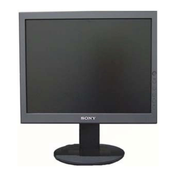
- Page 1 S95E Sony Service Manual TFT LCD COLOR COMPUTER DISPLAY SONY...
-
Page 2: Table Of Contents
S95E Sony Table of contents Table of contents -------------------------------------------------------------------------- 02 1. Precaution ------------------------------------------------------------------------------------------ 03 2 . S p e c i f i c a t i o n - - - - - - - - - - - - - - - - - - - - - - - - - - - - - - - - - - - - - - - - - - - - - - - - - - - - - - - - - - - 0 5 2.1 Product character-----------------------------------------------------------05... -
Page 3: Precaution
S95E Sony 1. Precaution Warning on power connections Installation... - Page 4 S95E Sony Handing the LCD screen Maintenance Transportation...
-
Page 5: S P E C I F I C A T I O
S95E Sony 2. Specification 2.1 Product character Driving system TFT LCD Size 19.0" Type M190EN04 V5 Pixel pitch (0.098 x 3 )mm(H) x 0.294mm(V) Viewing angle 170(H) 170(V) Luminance 300 cd/m (typ) LCD Panel Contrast Ratio 600:1 (typ) Response time... -
Page 6: Interface Description
S95E Sony 2.2 Interface description 1. HD 15 Signal Input Pin Assignments Description Description Red Video Green Video(Sync on Green) Sync Return Blue Video ID (GND) ID(GND) DDC Data Sense of connection PC Horizontal Sync Red Video Return Vertical Sync... -
Page 7: Factory Preset Mode
S95E Sony 2.3 Factory preset mode Clock (MHZ) Resolution Frequency (KHz) Vertical (Hz) 28.322 720 × 400 31.469 70.087 25.175 640 × 480 31.469 59.940 30.240 640 × 480 35.000 66.667 31.500 640 × 480 37.500 75.000 31.505 720 × 480 35.200... -
Page 8: Osd Operation
S95E Sony 3. OSD operation 3.1 Generalization Press the power button to turn the monitor on or off. The other control buttons are located at front panel of the monitor. By changing these settings, the picture can be adjusted to your personal preferences. -
Page 9: Common Adjustment
S95E Sony Key control: 3.3 Common adjustment Icon Description Backlight Adjust the brightness of the backlight Contrast Adjust the picture contrast Brightness Adjust the picture brightness (black level) Screen Adjust the picture’s sharpness or its centering Color Adjust the color temperature of the picture γ... - Page 10 S95E Sony Adjustment steps of each menu...
- Page 11 S95E Sony...
- Page 12 S95E Sony...
- Page 13 S95E Sony...
- Page 14 S95E Sony...
- Page 15 S95E Sony...
- Page 16 S95E Sony...
- Page 17 S95E Sony...
- Page 18 S95E Sony...
- Page 19 S95E Sony...
-
Page 20: Adjustment
30 minutes for RGB reset before W/B adjustment. 2. Setup 1) Prepare timing and pattern data for a signal generator according to the Sony timing specifications. 2) Connect a monitor video cable to the signal generator. -
Page 21: Service Osd
S95E Sony 5. Adjustment for White Balance a. Display SMPTE at SXGA/60Hz(Input level 0.73V). b. Set up [SERVICE MODE]. c. Click "CLEAR EEPROM" and AC Power off. d. Set up [SERVICE MODE] of the monitor again. e. Click "WHITE BALANCE" and then select "AUTO". -
Page 22: Disassembly Flow Chart
S95E Sony I). LIGHT SENSOR : When ECO Auto mode,the BACKLIGHT is changed as Light sensor input X :Light Sensor input, Y : Backlight Value setting, j). VCTi DEBUG : VCTi can be setted on DEBUG on/off, When you want to controll anything. - Page 23 S95E Sony Step2 Figure Description Discharge the base 1, Wring the five screws in the bracket marked in red. 2, Take the screw and stand away 3. Steel line marked in green is to rise or lower the stand. Wring the screw...
- Page 24 S95E Sony 1, insert a hard plastic chip in the gap between bezel and rear cover at up-left corner 2, Hold the monitor with a hand and press the hard plastic chip with the other, then move it in the forward hour hand.
- Page 25 S95E Sony 1,Wring down the four screws marked Discharge the in red. 2, Pull out the lamp and main board power board connection lines marked in yellow 1, Wring the four screws marked with red. Discharge the 2, Pull out the other connection lines...
-
Page 26: Wiring Diagram
S95E Sony The panel is disassembled absolutely. 4.2 WIRING DIAGRAM... -
Page 27: Monitor Exploded View
S95E Sony 4.3 Monitor Exploded View... -
Page 28: Circuit Principle Analysis
S95E Sony 5. Circuit principle analysis The LCD Monitor contains a main board, an inverter/power board, keyboard which house the flat panel control logic, brightness control logic and DDC. Backlight and Panel PWPC board Main board Key board Video signal and DDC HOST computer 5.1 Main board... -
Page 29: Introduction Of
S95E Sony 5.1.2 Introduction of IC GM5321: integrate ADC, OSD, SCALER, MCU, LVDS, convert analog RGB into digital and zoom and shrink scaling output to LCD panel. AIC1084-33M: DC power convert, used to 5v convert 3.3v. AIC1084-18CE: DC power convert, used to 5v convert 1.8v. - Page 30 S95E Sony Panel Control Circuit: The high level output from PIN67 of U201 makes Q402 break through, Q203 break through and offer 5V to panel when work well. The output is low level when it’s saving energy state and Q402 break off, Q203 break off, so the panel doesn’t work.
-
Page 31: Pwpc Board
S95E Sony Interface of main board and PWPC board 5.2 PWPC board 5.2.1 Block diagram PWPC board combines to adapter and inverter, this design has the merits in predigesting constructions, reducing cost and improving product’s capability. Adapter which commonly consists of bridge rectifier and filter, start circuit, PWM control circuit (TOP247Y), protection circuits and convert to 12V, 5V DC voltage by input 90V-240V AC voltage that provide power supply for each chips in the main board and inverter. -
Page 32: Introduction Of
S95E Sony 5.2.2 Introduction of IC TOP247Y: It cost effectively integrating the high voltage power MOSFET, PWM control, fault protection and other control circuitry onto a single CMOS chip. The function of each pin and the inside circuit diagram are as... -
Page 33: Introduction Of Important Function
S95E Sony BA9741F: PWM control, voltage range for working: 3.6~35V, Has such functions as short-voltage protection, Over-voltage protection, over-current protection and etc. The function of each pin and the circuit diagram inside are as follows: NAME FUNCTION NAME FUNCTION External timing capacitor... - Page 34 S95E Sony 1.414 to AC after it is commuted by bridge rectifier (BD901) and filtered by the capacitance (C905). Start-up circuit: After being commuted and filtered, the high DC voltage falls down through R (R904, R908, and R911 series), the start-up carries out when the lowered voltage is supplied to L Pin of IC901 (TOP247Y).
- Page 35 S95E Sony C Pin of IC901 2. ZD901, ZD902 can be broken down when12V and 5V DC voltage increase, which lead to SCR901 breaks through, then 12 connected to ground and realizes over-voltage protection. Commute and filter output circuit: When D Pin of IC901 has pulse output, which makes T901 work, while being given a low level, and there is a current in the primary coil of T901 with a voltage up terminal positive and down negative, so the secondary coil produces a reverse electromotive force.
- Page 36 S95E Sony level, The primary coil produces a EMF with its down terminal positive and up negative, and the secondary coil appears a reverse EMF at the same time, then D902, D904 get through accompanied with a voltage output of 12V and 5V through C904, C909 which are used to filter.
- Page 37 S95E Sony PIN9 of U201 Protection circuit: 1. Over-voltage protection: D203 or D204 is broken down when the output of L201 or L202 exceeds 11V, which increases the voltage applied across R222 or R223.It results in rising the DTC value of U201.When the value falls downs to be lower than surge voltage, the output is shut.
- Page 38 S95E Sony From U201 PIN10 TO U201 PIN11 OSC and output circuit: OSC is made up of C213 and PT201 and PUSH-PULL circuit is made up of Q209, Q210. They are in alternate working state. R224, R225, R226, R227 are used for starting up OSC. The voltage of Q209 and Q210 adds in PT201, and then it produces high voltage sine wave through LC OSC.
- Page 39 S95E Sony...
-
Page 40: Trouble Shooting
S95E Sony 6. Trouble shooting 6.1 Main board No power No power Press power key and look if the picture is normal Please reinsert and make sure the AC of 100-240 is normal Reinsert or check the power section Measure U602 PIN2=3.3V C609(+)=1.8V... - Page 41 S95E Sony No picture (LED orange) No picture Measure U602 PIN2=3.3V C609(+)=1.8 Check Correspondent component X301 oscillate waveform is normal Check Correspondent component. Replace U301...
- Page 42 S95E Sony White screen White screen Measure Q502 base is high level? Measure U602 PIN2=3.3V C609 (+) =1.8V Check Q502 and Q501 are Check Correspondent broken or CN501 solder? component X301 oscillate waveform is normal Check Correspondent component Check Correspondent...
-
Page 43: Pwpc Board
S95E Sony 6.2 PWPC board No Power Check to CN902 Pin5=12.0V and pin9 = 5.0V Check Interface board Check AC line voltage 110V or 240V Change F901 , check BD901,Q903,IC901 Check the voltage of C905(+) Check bridge rectified circuit Check start voltage for the pin3 of IC901... - Page 44 S95E Sony No Backlight Check VDDA,ENA VDDA=4.75~5.25V;ENA>3V Check On/Off loop Circuit Preset at 2V to SST(pin4) of IC801 and Connect CTIMR(Pin1) to GND Check REF (pin7), RT (pin17), CT(pin18),NDRV_D(pin11), PDRV C(pin12),PDRV A(pin19),NDRV B(pin20) of IC801 Check full bridge power conversion...
-
Page 45: Bom
S95E Sony 7. BOM 7.1 T982KADDKNSVAP Symbol Part NO. for TPV Description M1G1730 6120 GP M3*6 SCREW AUPC982S1P AUDIO BOARD CBPC982KAD1SP CONVERSION BOARD PWPC1942CMS1P POWER BOARD 6 5S02 GP COMPOUND PALLET 11G6048 1 CLAMP-S 11G6054 1 LOCK WASHER 11G6070 1... - Page 46 S95E Sony M1G 130 4120 GP CPT PANEL/MAINFRAME M1G 130 6120 GP SCREW M1G 240 12225 GP SCREW M1G 330 4 47 GP SCREW M1G 330 4120 GP SCREW M1G1140 6120 GP SCREW M1G1730 6120 GP M3*6 SCREW Q1G 330 8120 GP...
- Page 47 S95E Sony C501 67G305V101 4N GP KME25VB100M-CC3 6.3*1 C601 67G215L101 4N GP KY25VB100M-L(6.3*11) C604 67G215L470 4N GP KY25VB47M-L 5*11 C605 67G215L470 4N GP KY25VB47M-L 5*11 C608 67G215Y2207NV GP KY50VB22M-CC3 C609 67G215V221 4N GP KY25VB220-M-CC3 C702 67G215L470 4N GP KY25VB47M-L 5*11...
- Page 48 S95E Sony C307 65G0603104 12 GP CHIP 0.1UF 16V X7R C308 65G0603104 12 GP CHIP 0.1UF 16V X7R C310 65G0603104 12 GP CHIP 0.1UF 16V X7R C311 65G0603104 12 GP CHIP 0.1UF 16V X7R C312 65G0603104 12 GP CHIP 0.1UF 16V X7R...
- Page 49 S95E Sony C611 65G0603102 32 GP 1000PF +-10% 50V X7R C612 65G0603102 32 GP 1000PF +-10% 50V X7R C613 65G0603102 32 GP 1000PF +-10% 50V X7R C614 65G0603102 32 GP 1000PF +-10% 50V X7R C615 65G0603104 12 GP CHIP 0.1UF 16V X7R...
- Page 50 S95E Sony Q204 57G 759 2 RK7002 Q205 57G 758 1 2N7002ESOT23 SILICONIX Q205 57G 759 2 RK7002 Q401 57G 417 4 PMBS3904/PHILIPS-SMT(04 Q402 57G 417 4 PMBS3904/PHILIPS-SMT(04 Q501 57G 763 1 A03401 SOT23 BY AOS(A1) Q502 57G 417 4...
- Page 51 S95E Sony R315 61L0603472 CHIPR 4.7K OHM +-5% 1/1 R316 61L0603472 CHIPR 4.7K OHM +-5% 1/1 R317 61L0603472 CHIPR 4.7K OHM +-5% 1/1 R318 61L0603472 CHIPR 4.7K OHM +-5% 1/1 R323 61L0603472 CHIPR 4.7K OHM +-5% 1/1 R324 61L0603472 CHIPR 4.7K OHM +-5% 1/1...
- Page 52 S95E Sony R702 61L0603000 CHIPR 0OHM +-5% 1/10W R703 71G 59B121 CHIP BEAD 1200HM R704 71G 59B121 CHIP BEAD 1200HM R716 71G 59B121 CHIP BEAD 1200HM R717 71G 59B121 CHIP BEAD 1200HM R722 61L0603000 CHIPR 0OHM +-5% 1/10W R723 61L0603000...
- Page 53 S95E Sony 15G8033 1 BKT_AC INLET 40G 45762420A GP CBPC LABEL 25X6mm 1174 TYPE M1G1730 6128 GP SCREW 705G 780 61 58 NR901 ASS'Y 705G 780 87 27 CN901 ASS'Y 705G 780 93 S2 D904 ASS'Y 705G 780 93 S9...
- Page 54 S95E Sony L902 73L 174 55LSG GP LINE FILTER BY LISHIN L903 73G 253 91 LS GP CHOKE BY LI SHIN L904 73G 253 91 LS GP CHOKE BY LI SHIN PT801 80LL17T 16DNG GP INVERTER TRANSFORMER PT801 80LL17T 16LCG GP...
- Page 55 S95E Sony C813 65G1206104 32 GP CHIP 0.1UF 25V X7R 1206 C815 65G0805222 31 GP CHIP 0.0022UF 50V NPO 0 C817 65G0805222 31 GP CHIP 0.0022UF 50V NPO 0 C819 65G0805105 22 GP CHIP 1UF 25V X7R 0805 C820 65G1206104 32 GP CHIP 0.1UF 25V X7R 1206...
- Page 56 S95E Sony D809 93G 6432V LL4148-GS08 D810 93G 64 33 DIO SIG SM BAV99 (PHSE) D810 93G 6433G BAV99-SMT D812 93G 64 33 DIO SIG SM BAV99 (PHSE) D812 93G 6433G BAV99-SMT D813 93G 64 33 DIO SIG SM BAV99 (PHSE)
- Page 57 S95E Sony Q810 57G 600 60 MOSFET Q810 57G 60040A AM4512C-T1-PF SO-8 Q811 57G 600 40 SP8M3FTB SOP-8 Q811 57G 600 60 MOSFET Q811 57G 60040A AM4512C-T1-PF SO-8 Q812 57G 417 4 PMBS3904/PHILIPS-SMT(04 Q812 57G 417 4A 2SC3052-T112-1F Q901 57G 417 6...
- Page 58 S95E Sony R837 61L0805102 CHIPR 1K OHM +-5% 1/8W R838 61L1206471 CHIP 470 OHM 1/8W R840 61L0805104 CHIPR 100K OHM+-5% 1/8W R842 61L0805104 CHIPR 100K OHM+-5% 1/8W R843 61L0805104 CHIPR 100K OHM+-5% 1/8W R844 61L1206220 22 OHM/1206 R845 61L0805220 CHIP 22 OHM 5% 0805 1/8...
- Page 59 S95E Sony R937 61L1206101 CHIP 100 OHM 5% 1/4W ZD801 93G 39S 24 T RLZ 5.6B LLDS ZD802 93G 39S 24 T RLZ 5.6B LLDS ZD805 93G 39S 24 T RLZ 5.6B LLDS ZD901 93G 39S 41 T RLZ24B LLDS...
- Page 60 S95E Sony JP816 95G 90 23 TIN COATED JP818 95G 90 23 TIN COATED JP819 95G 90 23 TIN COATED JP820 95G 90 23 TIN COATED JP821 95G 90 23 TIN COATED JP822 95G 90 23 TIN COATED JP823 95G 90 23...
- Page 61 S95E Sony NR901 61G 58080 WT GP 8 OHM NCTR 52G6025 12113 GP MYLAR CN901 87G 501 27 RF GP AC SOCKET 90G6241 1 HEAT SINK AM1G1730 8128 GP SCREW M3*8 D904 93G 60248 SP20100 90G6241 2 HEAT SINK AM1G1730 8128 GP...
- Page 62 S95E Sony Q1G1030 6120 GP SCREW SM1G 140 6125 GP SCREW W33G4881 LO L GP KEPC982KS2P Symbol Part NO. for TPV Description AIK982KS1SMTP KEY BOARD 715G1518 1 CN101 33G8034 9A WAFER DP101 81G 14 6 KT GP KEL-HJDGE33B-TRB SW101 77G 605 1 AL GP...
-
Page 63: Schematic
S95E Sony 8. Schematic... - Page 64 S95E Sony...
- Page 65 S95E Sony...
- Page 66 S95E Sony...
- Page 67 S95E Sony...
- Page 68 S95E Sony...
- Page 69 S95E Sony...