
Related Manuals for Sony WRR-802A


Summary of Contents for Sony WRR-802A
- Page 1 UHF SYNTHESIZED DIVERSITY TUNER WRR-802A SERVICE MANUAL U Model 1st Edition Printed in Japan Sony Corporation WRR-802A (U) E 1999. 6 11 Broadcasting & Professional Systems Company 9-976-876-01 ©1999...
- Page 2 électrique, d’incendie ou de blessure n’effectuer que les réparations indiquées dans le mode d’emploi à moins d’être qualifié pour en effectuer d’autres. Pour toute réparation faire appel à une personne compétente uniquement. WRR-802A (U)
-
Page 3: Table Of Contents
Electrical Parts List ..................5-4 5-4. Accessories Supplied ................5-12 6. Block Diagrams Overall Block Diagram ................6-2 Tuner Unit Block Diagram ................6-3 7. Board Layouts CN-1922 Board ................... 7-1 CN-1923 Board ................... 7-1 MB-872 Board .................... 7-2 WRR-802A (U) - Page 4 RF-92 Board (Tuner unit) ................7-3 8. Schematic Diagrams CN-1922 Board ................... 8-1 CN-1923 Board ................... 8-2 MB-872 Board .................... 8-2 RE-176 Board ....................8-2 VR-261 Board ..................... 8-2 DP-305 Board (Tuner unit) ................. 8-6 RF-92 Board (Tuner unit) ................8-4 WRR-802A (U)
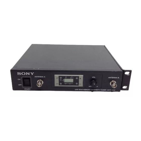
- Page 5 Record the serial number in the space provided below. including the levels of the reception channels, RF allocated for UHF TV broadcasting. Refer to them whenever you call upon your Sony dealer information and transmitter battery condition. Trade Name :...
- Page 6 2 AF (audio frequency) level indications To go to a lower group or channel, press this button while The unit can be used with a Sony UHF synthesized wireless holding the GP or CH button. The indicator lights and the indications appear when the microphone or UHF synthesized transmitter among the audio output level is higher than the reference level.
- Page 7 3 m (9 feet 11 inches). selected. • When adding the WRR-802A by cascade connection to a • The number of wireless microphone channels actually tuner system containing the WD-820A UHF Antenna usable in a multi-channel system may be smaller than the –...
- Page 8 ON. All indications momentarily appear, then go off. uno de los grupos originales de Sony, es decir, los número Les autres groupes sont inclus pour satisfaire aux “OFF” is then displayed. This procedure cancels all three 00, 11, 12, 13, A1, A2, A3, L1, L2, H1 o H2.
- Page 9 Group 11: 11-channel group Group 12: 8-channel group Group 13: 8-channel group Group L1: 7-channel group Group L2: 7-channel group Group H1: 7-channel group Group H2: 7-channel group Use when both TV channels 68 and 69 Use when TV channel 69 is open. Use when TV channel 68 is open.
- Page 10 Group 12: 8-channel gruop Group 13: 8-channel group Group L1: 7-channel group Group L2: 7-channel group Group H1: 7-channel group Group H2: 7-channel group Group 11: 11-channel group Use when TV channel 67 is open. Use when TV channel 66 is open. Use when TV channel 66 is Use when TV channel 66 is Use when TV channel 67 is...
- Page 11 Group 11: 11-channel group Group 12: 8-channel group Group 13: 8-channel group Group L1: 7-channel group Group L2: 7-channel group Group H1: 7-channel group Group H2: 7-channel group Use when both TV channels 64 and 65 Use when TV channel 64 is open. Use when TV channel 65 is open.
-
Page 13: Service Overview
RE-176 Tuner Unit VR-261 DP-305 RF-92 2-2. Error Messages The following error messages will appear if an error is detected by the built-in self diagnostics function of the WRR-802A. Error message Comments Countermeasure Err 01 Error the backup memory Because data is initialized, perform the group setting, channel setting again. -
Page 14: Setting / Release Of Muting Function
2-3. Setting / Release of Muting Function Set or release the following functions by operating the button on the front panel of the WRR-802A. Function Setting / Release . Muting OFF by RF signal input level Muting OFF mode setting: . -
Page 15: Tuner Unit Checking
2-4-2. Tuner Unit Checking The following procedures describe how to prove the tuner unit of WRR-802A (repair unit) whether it needs to be repaired or not. Equipment Required : MB-806A (quality unit) WRU-806A (quality unit) (1) Install the repair tuner unit to be examined in a quality MB-806A. -
Page 17: Electrical Alignment
(sine wave) can be generated. Mic amp Gain: 0 dB to 70 dB (with A weighted filter) — Oscilloscope Frequency: DC to 30 MHz — Tools Name Part No. Remarks Adjuster (0.4 x 1.3 mm) 7-721-052-81 For adjustment WRR-802A (U) -
Page 18: Adjustment
Adjust the output of 100 dBu the signal generator (SSG) so that the = _113 dBm 0 dBuV 50 Z meter reads 50 mV. (EMF = Electromotive force) 50 Z 50 mV 0 dBm = 1 mW at 50 Z loaded WRR-802A (U) - Page 19 3. Remove the upper side case lid of the tuner unit, and (1) Connect the signal generator to the ANTENNA A IN insert the tuner unit to the slot of the WRR-802A. connector. (2) Turn OFF the WRR-802A POWER switch.
- Page 20 (21)Indication on the LCD appears as follows: (A C3 L) LCD: (12)Set the FREQUENCY (carrier frequency) of the signal B C3 L generator as follow. FREQUENCY (carrier frequency) (B C3 L) U64 model; 780.000 MHz U66 model; 792.000 MHz U68 model; 804.000 MHz WRR-802A (U)
- Page 21 2. Remove the tuner unit from the WRR-802A. LCD: 3. Remove the upper side case lid of the tuner unit, and insert the tuner unit to the slot of the WRR-802A. • U64 model Equipment and Tools . DC power supply: +9 Vdc .
- Page 22 5. Attach the lower side case lid to the tuner unit, and (4) Connect the signal generator to the ANTENNA B IN insert the tuner unit to the slot of the WRR-802A. connector. (5) Adjustment (ANTENNA B IN side adjustment)
- Page 23 Procedure Step 3. Step 1: S/N check After completing adjustment, turn off the WRR-802A Perform the “ 2. S/N Check ” of Section 3-2-2. Overall power switch and perform the followings. Characteristics Check. (1) Remove the tuner unit from the WR-802A.
-
Page 24: Overall Characteristics Check
↓ 1. Output level check 3. Frequency characteristic check ↓ Procedure 4. Distortion check (1) Set the WRR-802A as follows; ↓ Channel setting: 5. RF Level indicator check U64 model; Group 00, 6501 channel (776.125 MHz) ↓ U66 model; Group 00, 6701 channel (788.125 MHz) 6. - Page 25 (13)Connect the audio analyzer to the TUNER OUTPUT (TRS type) connector via the MIC amp (Amplification Procedure gain 0 dB). (1) Set the WRR-802A as follows; (14)Perform the procedures (5) through (12). Channel setting: (15)Connect the signal generator to the ANTENNA B IN U64 model;...
- Page 26 3. Frequency characteristic check 4. Distortion ratio check Procedure Procedure (1) Set the WRR-802A as follows; (1) Set the WRR-802A as follows; Channel setting: Channel setting: U64 model; Group 00, 6501 channel (776.125 MHz) U64 model; Group 00, 6501 channel (776.125 MHz) U66 model;...
- Page 27 1 and 2 below. Procedure Perform the procedures (1) to (9) above, for each (1) Set the WRR-802A as follows; channel setting (1 and 2). Channel setting: 1 Channel setting: U64 model; Group 00, 6501 channel (776.125 MHz) U64 model: Group 00, 6401 channel (770.125 MHz)
- Page 28 1 and 2 below. Procedure Perform the procedures (2) through (5) above, for each (1) Set the WRR-802A as follows; channel setting (1 and 2). Channel setting: 1 Channel setting: U64 model; Group 00, 6501 channel (776.125 MHz) U64 model: Group 00, 6401 channel (770.125 MHz)
- Page 29 (9) Set the channel setting and FREQUENCY (carrier frequency) of the signal generator as shown 1 and 2 Procedure below. (1) Set the WRR-802A as follows; Perform the procedures (1) to (8) above, for each channel setting (1 and 2). Channel setting: 1 Channel setting: U64 model;...
- Page 30 8. BATT (Battery) indicator check 9. Tone squelch check Procedure Procedure (1) Set the WRR-802A as follows; (1) Set the WRR-802A as follows; Channel setting: Channel setting: U64 model; Group 00, 6501 channel (776.125 MHz) U64 model; Group 00, 6501 channel (776.125 MHz) U66 model;...
- Page 31 S-80735SN-DZ-T1 ... 4-5 S-81250SGUP-DQD-T1 ... 4-5 UMX2NTL ......4-2 SA575DK-T ...... 4-5 UN9213 ......4-2 TA31161FN(EL) ....4-5 TA78L05F-TE12L .... 4-4 TA8122AF ......4-5 TA8122AF(J.TP2) .... 4-5 TC4S69F ......4-6 TC4S69F(TE85R) .... 4-6 TC74HC4053AFT(EL) ..4-6 UPC4574G2-E2 ....4-6 WRR-802A (U)
- Page 32 —TOP VIEW— 2SB1202FAT-TL DTC323TK (R1=2.2 k) DTC323TKT146 EC10QS-04 EC10QS04-TE12L5 —TOP VIEW— MTD20N06HDLT4 2SC4726LN-TLPQ 2SC4738-YGR-TE85L 2SC4915-O-TE85L 2SD1048-X7 2SD1048X6-TB —TOP VIEW— 2SD2216-Q (TOSHIBA) HZU5.6B2TRF HZU6.8B2TRF —TOP VIEW— 2SJ377(TE16L) RN1104-TE85L UN9213 —TOP VIEW— RB411D RB411D-T146 SB07-03C SB07-03C-TB —TOP VIEW— UMX2NTL 3SK239AXRTL WIDE WRR-802A (U)
- Page 33 = 3.5V to 36V (SINGLE-SUPPLY TYPE) = 1.5V to 33V —TOP VIEW— ) = 1.26x (1+ ) (V) ( R1 = 4.3K , V = 1.26V) NJM4558V-TE2 (JRC) NJM4560M (JRC) NJM4560M-TE2 NJM5532M(TE2) (JRC) DUAL OPERATIONAL AMPLIFIERS (DUAL-SUPPLY TYPE) —TOP VIEW— WRR-802A (U)
- Page 34 OLA, B 14-BIT LATCH (REFERENCIAL DIVISION) P3/fr2 SELECTOR P1/fp1 P2/fp2 POWER SAV- 17-BIT LATCH (COMPARISONAL DIVISION) MAIN COUNTER PHASE CHARGE fin2 PLL2 P1, 2, 3 OLA, B 10-BIT LATCH CR1, 2 LATCH SELECTOR Data SHIFT REGISTER (21-BIT) Clock WRR-802A (U)
- Page 35 C OB C OB C OB C OB C OB C OB C OB C OB GAIN CELL GAIN CELL LATCH SOUT C OB C OB C OB C OB C OB C OB C OB C OB WRR-802A (U)
- Page 36 1 : HIGH LEVEL TC74HC4053AFT(EL) (TOSHIBA) C-MOS TRIPLE 2-CHANNEL ANALOG MULTIPLEXER/DEMULTIPLEXER —TOP VIEW— OPEN OPEN OPEN CONTROL INPUTS SELECT ON CHANNEL : LOW LEVEL : HIGH LEVEL OPEN : DON’T CARE UPC4574G2-E2 (NEC) QUAD OPERATIONAL AMPLIFIER —TOP VIEW— WRR-802A (U)
- Page 37 CH operation button PE5/PWM0 + operation button PE6/T0/ADJ _ operation button PD4/SEG20 SQL SET RSSI learning mode setting PD5/SEG21 Reset (L: ON) PD6/SEG22 PD7/SEG23 PE1/INT1 Connect to GND PE4/RMC Connect to GND Connect to GND — Connect to GND WRR-802A (U)
-
Page 39: Spare Parts
Therefore, specified parts should be used in the case of replacement. 2. Standardization of Parts Some repair parts supplied by Sony differ from those used for the unit. These are because of parts common- ality and improvement. Parts list has the present standardized repair parts. -
Page 40: Exploded Views
2-545-442-01 s GASKET (T1) (PUR) 2-545-443-01 s GASKET (T2) (PUR) 2-545-450-01 o INSULATING SHEET (CN) 2-545-768-01 o SHEET (REAR) 4-382-854-01 s SCREW +PSW 3X8 (STEEL) 4-942-568-41 s EMBLEM (N0.5), SONY 9-911-844-99 s SHEET, SPONGE Accessory 1-501-952-11 s ANTENNA Screws/Washers 7-682-246-09 s SCREW +K 3X5 (EP-FE/ZNBK/CM2) - Page 41 BVTT 3x6 BTP 3x8 BVTT 3x6 BVTT 3x6 K 3x5 BVTT 2.6x5 K 3x5 BVTT BVTT 3x6 K 3x5 BVTT 2 x 4 BVTT2 x 4 WRR-802A (U)
-
Page 42: Electrical Parts List
1-216-797-11 s RESISTOR,CHIP 10 1/16W 1608 R2117 1-216-803-11 s RESISTOR,CHIP 33 1/16W 1608 R2118 1-216-800-11 s RESISTOR,CHIP 18 1/16W 1608 R2119 1-216-803-11 s RESISTOR,CHIP 33 1/16W 1608 R2301 1-216-864-11 s RESISTOR,CHIP 0 1/16W (1608) R2401 1-216-864-11 s RESISTOR,CHIP 0 1/16W (1608) WRR-802A (U) - Page 43 C1121 1-136-153-00 s CAPACITOR,FILM 0.01MF/50V C1125 1-164-218-11 s CAPACITOR,CERAMIC 180PF/50V CH C1201 1-128-548-11 s CAPACITOR,ELECT 4700MF/25V C1202 1-164-004-11 s CAPACITOR,CERAMIC 0.1MF/25V C1203 1-164-004-11 s CAPACITOR,CERAMIC 0.1MF/25V C1204 1-113-981-11 s CAPACITOR TANTALUM 22MF/20V C1205 1-113-981-11 s CAPACITOR TANTALUM 22MF/20V WRR-802A (U)
- Page 44 1-216-821-11 s RESISTOR,CHIP 1.0K 1/16W 1608 L1006 1-424-618-11 s FILTER,NOISE R1206 1-216-105-91 s RESISTOR,CHIP 220K 1/10W(2125) R1207 1-216-833-11 s RESISTOR,CHIP 10K 1/16W 1608 Q1001 8-729-822-84 s TRANSISTOR 2SB1202FAST R1307 1-218-718-11 s RESISTOR CHIP 12K 1/16W (1608) Q1002 8-729-041-36 s TRANSISTOR MTD20N06HDLT4 WRR-802A (U)
- Page 45 1-107-826-11 s CAPACITOR,CHIP CERAMIC 0.1MF C186 1-162-920-11 s CAPACITOR,CERAMIC 27PF/50V CH C187 1-162-915-11 s CAPACITOR,CERAMIC 10PF/50V CH C200 1-107-826-11 s CAPACITOR,CHIP CERAMIC 0.1MF C201 1-135-177-21 s CAPACITOR TANTALUM 1MF/25V C202 1-117-919-11 s CAPACITOR, CHIP TANTALUM10MF C203 1-162-927-11 s CAPACITOR,CERAMIC 100PF/50V CH WRR-802A (U)
- Page 46 1-162-964-11 s CAPACITOR,CERAMIC 1000PF/50V B C291 1-104-851-11 s CAPACITOR,TANTALUM 10MF/10V C461 1-107-826-11 s CAPACITOR,CHIP CERAMIC 0.1MF C292 1-104-851-11 s CAPACITOR,TANTALUM 10MF/10V C462 1-107-826-11 s CAPACITOR,CHIP CERAMIC 0.1MF C302 1-162-907-11 s CAPACITOR,CERAMIC 2PF/50V(CK) C463 1-107-826-11 s CAPACITOR,CHIP CERAMIC 0.1MF WRR-802A (U)
- Page 47 1-104-851-11 s CAPACITOR,TANTALUM 10MF/10V IC203 8-759-278-58 s IC NJM4558V (TE2) C756 1-162-970-11 s CAPACITOR CERAMIC 0.01MF/25V B C757 1-162-927-11 s CAPACITOR,CERAMIC 100PF/50V CH IC204 8-759-278-58 s IC NJM4558V (TE2) C780 1-162-919-11 s CAPACITOR,CERAMIC 22PF/50V CH IC205 8-759-278-58 s IC NJM4558V (TE2) WRR-802A (U)
- Page 48 1-412-979-21 s INDUCTOR (SMALL TYPE) R210 1-216-827-11 s RESISTOR, CHIP 3.3K 1/16W 1608 L653 1-412-979-21 s INDUCTOR (SMALL TYPE) R211 1-216-832-11 s RESISTOR,CHIP 8.2K 1/16W 1608 L654 1-414-470-31 s INDUCTOR, CHIP (J) 39NH R212 1-216-821-11 s RESISTOR,CHIP 1.0K 1/16W 1608 5-10 WRR-802A (U)
- Page 49 1-216-825-11 s RESISTOR,CHIP 2.2K 1/16W 1608 R427 1-216-797-11 s RESISTOR,CHIP 10 1/16W 1608 R275 1-216-854-11 s RESISTOR, CHIP 560K 1/16W R428 1-216-814-11 s RESISTOR,CHIP 270 1/16 1608 R276 1-216-833-11 s RESISTOR,CHIP 10K 1/16W 1608 R429 1-216-825-11 s RESISTOR,CHIP 2.2K 1/16W 1608 5-11 WRR-802A (U)
-
Page 50: Accessories Supplied
SWF401 1-760-028-11 s FILTER, SAW T101 1-406-784-21 s TRANSFORMER, IF T102 1-406-782-21 s TRANSFORMER, IF T103 1-411-494-11 s DETECTOR COIL (MPX) T401 1-406-784-21 s TRANSFORMER, IF T402 1-406-782-21 s TRANSFORMER, IF T403 1-411-494-11 s DETECTOR COIL (MPX) 5-12 WRR-802A (U) -
Page 51: Block Diagrams
. DP-305 board The DP-305 board is composed of display block and operation The WRR-802A is composed of tuner unit (RF-92, DP-305 board), control block. The display block has the LCD which indicates the various status of group and channels and the AF indicator power supply block, audio block, and following boards. -
Page 52: Overall Block Diagram
CN1102 Q2101 CN1102 RF Block MUTE CN111 IC1101 J1101 IC1101 IC1303 IC1302 AF Block RF Block IC1004 IC1005 Q2201 REG. REG. J1701 IC1001 +12V -12V L1006 J1001 DC-DC DC 9V IN ±15V CONVERTER CN1001 POWER SWITCH Overall Block Diagram WRR-802A... -
Page 53: Dp-305 Board (Tuner Unit)
AF (B) – 150.75MHz 10.7MHz CN101 FL101 Q101 FL102 SWF101 CF101 Q106 CF102 IC102 CF103 IC101 Ant. IN (5/5) Q104,105 Q102,103 RF Amp 1st Mixer SAWF 2nd Mixer IF Amp Discriminator BPF(CF) IF Amp BPF(CF) BPF(CF) Tuner Unit Block Diagram WRR-802A... - Page 55 CN-1922, CN-1923 CN-1922, CN-1923 Section 7 Board Layouts CN-1923 -A SIDE- 1-674-358-11 CN-1922 -A SIDE- 1-674-357-11 CN-1923 -B SIDE- 1-674-358-11 CN-1922 -B SIDE- 1-674-357-11 WRR-802A (U)
- Page 56 MB-872, RE-176, VR-261 MB-872, RE-176, VR-261 RE-176 RE-176 -A SIDE- -B SIDE- 1-674-360-11 1-674-360-11 MB-872 -A SIDE- 1-674-356-11 VR-261 VR-261 -A SIDE- -B SIDE- 1-674-359-11 1-674-359-11 MB-872 -B SIDE- 1-674-356-11 WRR-802A (U)
- Page 57 DP-305, RF-92 DP-305, RF-92 Tuner Unit FOR BOARD NO. SUFFIX:-12 RF-92 -A SIDE- 1-674-364-11 DP-305 -A SIDE- 1-674-365-11 FOR BOARD NO. SUFFIX:-12 DP-305 RF-92 -B SIDE- -B SIDE- 1-674-365-11 1-674-364-11 WRR-802A (U)
-
Page 59: Schematic Diagrams
CE69 AU66 Ref.No. C2102,C2202 C2111,C2211 L2103,L2203 8.2nH 8.2nH 8.2nH 6.8nH 6.8nH 8.2nH 8.2nH CN-1922 BOARD NO.1-674-357-11 NOTE • DC Voltage are taken with digital multimeter (input impedance 1 MΩ or more) under no-signal conditions. CN-1922 BOARD NO. 1-674-357-11 WRR-802A (U) - Page 60 IN_A IN_A Q1202 2SC4738-YG 14.4V 2SC4738-YG 6.2V 14.4V 0.7V C1208 C1207 R1206 C1206 C1201 C1203 220k C1202 4700 C1204 C1205 NOTE • DC Voltage are taken with digital multimeter (input impedance 1 MΩ or more) under no-signal conditions. WRR-802A (U)
- Page 61 • For measuring points (A to F), see the schematic diagram. 0.5% R1316 Q1302 BOARD NO. 1-674-358-11 DTC323TKT1 R1314 C1313 RE-176 5.1k 0.5% C1315 R1308 6.3V TP1012 0.5% IC1303(2/2) NJM5532M(T D1302 BOARD NO. 1-674-360-11 1SS362-TE8 IC1302(2/2) NJM4560M-T R1323 VR-261 MB-872 BOARD N0.-1-674-356-11 BOARD NO. 1-674-359-11 WRR-802A (U)
-
Page 62: Board (Tuner Unit)
8.2nH 8.2nH 6.8nH 8.2nH 8.2nH When C416 is removed. L401,L402 Receiving frequency +150.75MHz L103,L403 10nH 10nH 10nH 10nH 8.2nH 10nH 10nH L104,L404 6.8nH 6.8nH 6.8nH 6.8nH 5.6nH 6.8nH 6.8nH NM:NO MOUNT RF-92 (1/2) Tuner unit BOARD NO. 1-674-364-11 WRR-802A (U) - Page 63 CXP83416-050Q CXP83416-050Q CXP83416-050Q CXP83416-051Q CXP83416-051Q CXP83416-051Q CXP83416-050Q SR751 0Ω SR752 0Ω SR753 0Ω 0Ω RF-92 (2/2) SR754-757 SR758 0Ω 0Ω 0Ω SR759 0Ω 0Ω 0Ω 0Ω Tuner unit SR760 0Ω SR761 0Ω 0Ω BOARD NO. 1-674-364-11 NM:NO MOUNT WRR-802A (U)
- Page 64 C806 C808 AF_LED 0.01 0.01 0.01 0.01 C803 C805 C807 RF_LED 0.01 0.01 0.01 COM0 S801 S802 S803 S804 COM1 C801 COM2 0.01 COM3 TO/FROM CN702,RF-92 BOARD COM1 COM2 ND801 COM0 COM3 DP-305 Tuner unit BOARD NO. 1-674-365-11 WRR-802A (U)