Yamaha STAGEPAS 500 Service Manual
Hide thumbs
Also See for STAGEPAS 500:
- User manual ,
- Service manual (70 pages) ,
- Owner's manual (4 pages)
Table of Contents
Advertisement
STAGEPAS 500
SERVICE MANUAL
Speaker
Mixer
Speaker
CONTENTS(目次)
Specifications(総合仕様) ............................................... 3
Panel Layout(パネルレイアウト) .................................. 4
Dimensions(寸法図) ......................................................... 4
Circuit Board Layout(ユニットレイアウト) .............. 5
Disassembly Procedure(分解手順) ........................... 6
Lsi Pin Description(LSI端子機能表) ............................ 16
Ic Block Diagram(ICブロック図)................................. 18
Circuit Boards(シート基板図) ..................................... 19
Inspections(検査) ......................................................... 27
(アンプユニットの調整) ..................................................... 30
Factory Setting(出荷時の設定) .................................. 30
Trouble Shooting(トラブルシューティング) ............ 31
BLOCK DIAGRAM(ブロックダイアグラム)
Circuit Diagram(回路図)
PA
011840
200612-155400
HAMAMATSU, JAPAN
1
Copyright (c) Yamaha Corporation. All rights reserved. PDF
'07.01
Advertisement
Table of Contents

Related Manuals for Yamaha STAGEPAS 500


Summary of Contents for Yamaha STAGEPAS 500
- Page 1 CIRCUIT BOARDS(シート基板図) ........19 INSPECTIONS(検査) ............27 ADJUSTMENT OF AMPLIFIER UNIT (アンプユニットの調整) ............. 30 FACTORY SETTING(出荷時の設定) ........30 TROUBLE SHOOTING(トラブルシューティング) .... 31 PARTS LIST BLOCK DIAGRAM(ブロックダイアグラム) CIRCUIT DIAGRAM(回路図) 011840 200612-155400 HAMAMATSU, JAPAN Copyright (c) Yamaha Corporation. All rights reserved. PDF ’07.01...
- Page 2 IMPORTANT NOTICE This manual has been provided for the use of authorized Yamaha Retailers and their service personnel. It has been assumed that basic service procedures inherent to the industry, and more specifically Yamaha Products, are already known and understood by the users, and have therefore not been restated.
-
Page 3: Specifications
STAGEPAS 500 総合仕様 SPECIFICATIONS 一般仕様 General Specifications Maximum Output Power 最大出力 250 W+250 W (±10 %)/4 Ω @10 % THD at 1 kHz (SPEAKER L/R) 250W+250W(±10%)/4Ω @10% THD at 1kHz (SPEAKERS L/R) 200 W+200 W/4 Ω @1 % THD at 1 kHz (SPEAKER L/R) ≧200W+200W/4Ω... -
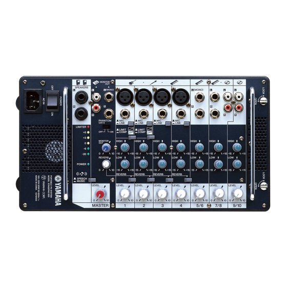
Page 4: Panel Layout
STAGEPAS 500 PANEL LAYOUT(パネルレイアウト) MASTER 9/10 q [AC IN] jack ([AC IN]端子) !0 [LIMIT/COMP] switches ([LIMIT/COMP]スイッチ) w [POWER] switch ([POWER]スイッチ) !1 Equalizer [HIGH]/[LOW] (EQ(イコライザー)) !2 [REVERB] switches ([REVERB]スイッチ) e [SPEAKERS L/R] jacks (for included speakers (500S) only) !3 [REVERB] control ([REVERB]コントロール) ([SPEAKERS L/R]端子(付属のスピーカ(500S)専用)) -
Page 5: Circuit Board Layout
STAGEPAS 500 CIRCUIT BOARD LAYOUT(ユニットレイアウト) Front view Right side view Speaker HF <Tweeter> (スピーカHF <ツィーター>) NETWORK POWER NETWORK CONTROL1 (1/3) CONTROL2 (2/3) CONTROL3 (3/3) JACK Speaker LF <Woofer> (スピーカLF <ウーファー>) Rear view POWER CONTROL2 (2/3) CONTROL1 (1/3) CONTROL3 (3/3) JACK... -
Page 6: Disassembly Procedure
STAGEPAS 500 (分解手順) DISASSEMBLY PROCEDURE フロントグリル Ass'y Front Grille Assembly (所要時間:約 1 分) (Time required: About 1 minute) [190]のネジ4本を外して、 フロントグリルAss'yを Remove the four (4) screws marked [190]. The front 外します。 (図 1) grille assembly can then be removed. (Fig. 1) スピーカLF (... - Page 7 STAGEPAS 500 Speaker LF (Woofer) Speaker HF (Tweeter) (スピーカLF(ウーファー)) (スピーカHF(ツィーター)) Wire LF (Red) Wire LF (Black) (束線LF(赤)) (束線LF(黒)) Wire HF (Yellow) Wire HF (Blue) (束線HF(黄)) (束線HF(青)) Photo 1 ( 写真 1) Photo 2 ( 写真 2) スピーカHF ( ツィーター) Speaker HF (Tweeter) (...
- Page 8 STAGEPAS 500 ミキサー Ass'y、カバーモールド Ass'y Mixer Assembly, Cover Mold Assembly (所要時間:約 1 分) (Time required: About 1 minute) Rotate the two (2) straight slots on the fastener コインドライバーまたはマイナスドライバーで、 heads with a coin driver or minus driver until each フ ァ ス ナ ー ヘ ッ ド の マ イ ナ ス 形 溝 2 箇 所 を...
- Page 9 STAGEPAS 500 リアケース Rear Case (所要時間:約 2 分) (Time required: About 2 minutes) ミキサー Ass'y を外します。 (6 項参照) Remove the mixer assembly. (See procedure 6) [400]のネジ 8本を外して、 ミキサー Ass'y からリア Remove the eight (8) screws marked [400]. The rear ケースを外します。 (写真 7)...
- Page 10 STAGEPAS 500 DSP シート DSP Circuit Board (所要時間:約 2 分) (Time required: About 2 minutes) 11-1 ミキサー Ass'y を外します。 (6 項参照) 11-1 Remove the mixer assembly. (See procedure 6) 11-2 リアケースを外します。 (8 項参照) 11-2 Remove the rear case. (See procedure 8) 11-3 シールドブラケット...
- Page 11 STAGEPAS 500 [260A] [260B] [260C] [260A] CONTROL3 (3/3) Phone bracket (ホーンブラケット) [260A], [260B], [260C]: Bind Head Tapping Screw-B(B タイト+ BIND)3.0X8 CR3 (AAX61980) Photo 13 ( 写真 13) Shield Bracket 1 Assembly シールドブラケット 1 Ass'y (所要時間:約 4 分) (Time required: About 4 minutes) 13-1 Remove the mixer assembly.
- Page 12 STAGEPAS 500 13-6 Disconnect the connectors CN801, CN802 and 13-6 POWER シートの CN801、CN802、CN803 と CN803 of the POWER circuit board and the connector CONTROL3 (3/3)シートの CN542 のコネクターを CN542 of the CONTROL3 (3/3) circuit board. The 抜いて、 シールドブラケット1 Ass'y (AMPシート、 shield bracket 1 assembly (including AMP circuit CONTROL3 (3/3)シート、...
- Page 13 STAGEPAS 500 14-6 Remove the CONTROL1 (1/3) circuit board from 14-6 CONTROL2 (2/3)シートのCN21、 CN26のコネクター the connectors CN21 and CN26 of the CONTROL2 から CONTROL1 (1/3)シートを外します。 (写真 20) ※ [120]のプッシュボタン 4 個と[130]のプッシュス (2/3) circuit board. (Photo 20) ペーサ4個は、 CONTROL1 (1/3)シートの構成部品 The four (4) push buttons marked [120] and four ではありません。...
- Page 14 STAGEPAS 500 15-8 Remove the five (5) screws marked [110]. The 15-8 [110]のネジ 5 本を外して、CONTROL2 (2/3)シー CONTROL2 (2/3) circuit board can then be トを外します。 (写真 23) ※ 以下の各部品は、 CONTROL2 (2/3)シートの構成部 removed. (Photo 23) 品ではありません。 CONTROL2 (2/3)シートを交換 The following parts are not parts of the す...
- Page 15 STAGEPAS 500 Soldering (半田付け) Power switch Panel (パネル) (電源スイッチ) Connector assembly (1P) (brown) (束線 1P (茶)) Earth wire (green) (アース線 (緑)) AC inlet (ACインレット) (blue) Soldering (brown) Power switch (半田付け) (青) (茶) (電源スイッチ) Connector assembly (2P) (束線 2P) Panel (パネル) Fig.3 ( 図...
- Page 16 STAGEPAS 500 (LSI端子機能表) LSI PIN DESCRIPTION YMW767-VTZ (X6055A00) CPU (SWL01B) DSP: IC1007 NAME FUNCTION NAME FUNCTION Ground Ground Input for TEST Power supply +3.3 V TESTN PLLBPN PLL bypass select External memory lower-byte enable / Port F LBN/LWRN/PF6 PLLV PLL Power supply +2.5 V...
- Page 17 STAGEPAS 500 AK5381VT (X8575A00) ADC (Analog to Digital Converter) DSP: IC1004 DAC1A: IC401 NAME FUNCTION NAME FUNCTION AINR Rch Analog input pin SDTO Audio serial data output pin AINL Lch Analog input pin LRCK Output channel clock pin CKS1 Mode select 1 pin...
-
Page 18: Ic Block Diagram
STAGEPAS 500 (ICブロック図) IC BLOCK DIAGRAM FA3641N (X8570A00) PWM Control POWER: IC803 6.5 A 0.82V~0.68V 15.5V – UVLO 15.5V 5V REF 0.9mA – RTRch – – 16.5V/9V 8.5V~7.9V 0.8V IS(+)/IS(-) 3.0V – OUTPUT – – – Dmax RM RT 0.24V –... -
Page 19: Circuit Boards
STAGEPAS 500 (シート基板図) CIRCUIT BOARDS AMP Circuit Board (4200-30) ..............26 CONTROL1 (1/3) Circuit Board (6486-30) ..........24 CONTROL2 (2/3) Circuit Board (6486-30) ......... 22/23 CONTROL3 (3/3) Circuit Board (6486-30) ..........25 DSP Circuit Board (1043-40) ..............19 JACK Circuit Board (5254B-30) ............... 25 NETWORK Circuit Board (5254A-30) ............ - Page 20 STAGEPAS 500 POWER Circuit Board Component side(部品側) 444598 (J, U, C), 444744 (B, H, O)
- Page 21 STAGEPAS 500 POWER Circuit Board Pattern side(パターン側) 444598 (J, U, C), 444744 (B, H, O)
- Page 22 STAGEPAS 500 CONTROL2 (2/3) Circuit Board Component side(部品側) 444603...
- Page 23 STAGEPAS 500 CONTROL2 (2/3) Circuit Board Pattern side(パターン側) 444603...
- Page 24 STAGEPAS 500 CONTROL1 (1/3) Circuit Board Component side(部品側) Pattern side(パターン側) 444603...
- Page 25 STAGEPAS 500 CONTROL3 (3/3) Circuit Board to CONTROL2 (2/3)-CN24 to POWER-CN804 Pattern side(パターン側) Component side(部品側) JACK Circuit Board to NETWORK-CN8 Component side(部品側) CONTROL3 (3/3): 444603 JACK: 445546...
- Page 26 STAGEPAS 500 AMP Circuit Board Pattern side(パターン側) to CONTROL3 (3/3)-CN544 (L ch) CONTROL3 (3/3)-CN546 (R ch) to CONTROL3 (3/3)-CN543 (L ch) CONTROL3 (3/3)-CN545 (R ch) Component side(部品側) NETWORK Circuit Board Component side(部品側) AMP: 444611 NETWORK: 445546...
- Page 27 STAGEPAS 500 (検査) INSPECTIONS Test Conditions(試験条件) Measuring Voitage(測定電圧): AC 100 V 50/60 Hz (J) AC 120 V 60 Hz (U, C) AC 230 V 50 Hz (B, H) AC 220 V 50 Hz (O) 4 Ω Load(負荷): Input(入力): 1 KHz MASTER LEVEL VR(マスターレベル...
- Page 28 STAGEPAS 500 ITEM INPUT CONDITIONS OUTPUT CONDITIONS NOMINAL LIMIT (項目) (入力条件) (出力条件) (標準値) (限界値) INPUT SENSITIVITY INPUT 1, 2, 3, 4 (Each) SP OUT: L, R -23 dBu -23 dBu±2 dB (入力感度) INPUT=XLR REF: 200 W OUTPUT INPUT-SW=LINE MONITOR OUT: -30 dBu -30 dBu±2 dB...
- Page 29 STAGEPAS 500 ITEM INPUT CONDITIONS OUTPUT CONDITIONS NOMINAL LIMIT (項目) (入力条件) (出力条件) (標準値) (限界値) CROSSTALK INPUT 1, 2, 3, 4, 5, 6, 7, 8 to SP OUT: 75 dB >70 dB (クロストーク) Adjacent INPUT REF: 1 KHz, 200 W OUTPUT (隣接...
- Page 30 STAGEPAS 500 Limiter Indication(リミッタ−表示の確認) The product shall be set to 32 dBu output on SP OUT. Then, LIMITER LED(RED) should light on and all LEDs of LEVEL meter should light on. (SP OUT に 32 dBu を出力させた時、LIMITER 表示 LED(赤色)が点灯し(一瞬でも可) 、LEVEL 表示 LED が全て...
-
Page 31: Trouble Shooting
STAGEPAS 500 (トラブルシューティング) TROUBLE SHOOTING ∗ ∗ ∗ ∗ ∗ Points marked by “ ” to “ ” in the figure of circuit board are the points to be checked as indicated by the same marks in the flowchart on the next page or after. - Page 32 STAGEPAS 500 Trouble Shooting (POWER circuit board) Note: Check and repair must be done carefully, otherwise the electrical shock may be caused. [ 注意:感電するおそれがありますので、注意して作業を行ってください。] START < Fuse: Primary > F801 (Fuse) OPEN ? < Power Supply: +VB > CN804: 1 pin <+VB>...
- Page 33 STAGEPAS 500 < Signal Path > < FAN > < Power LED > Connect the circuit boards("CONTROL1 (1/3)", "DSP", "CONTROL2 (2/3):CN542-CN24") and a fan. "CONTROL1(1/3)シート"、"DSPシート"、"CONTROL2(2/3)シート:CN542-CN24" 及び FAN を接続 Power LED=BLINKING [点滅] POWER switch: OFF Power LED=BLINKING [点滅] ( Q549: ON ) Power LED = ON [点灯]...
-
Page 34: Parts List
PARTS LIST CONTENTS(目次) OVERALL ASSEMBLY(総組立) ........2 MIXER ASSEMBLY(ミキサー Ass'y) ......5 ELECTRICAL PARTS(電気部品) ......8-26 Notes : DESTINATION ABBREVIATIONS A : Australian model M : South African model B : British model O : Chinese model C : Canadian model Q : South-east Asia model D : German model T : Taiwan model... - Page 35 STAGEPAS 500 OVERALL ASSEMBLY(総組立) ∗ [With mixer] Rear cabinet unit Bracket fastner 1 assembly Mixer assembly: (リアキャビネット部) (ブラケットファスナー1 Ass'y) See page 5. (ミキサーAss'y) J,B,H,O Bracket fastner 2 assembly models (ブラケットファスナー2 Ass'y) B,H models only U,C models only Rear cabinet assembly (リアキャビネットAss'y)...
- Page 36 STAGEPAS 500 PART NO. DESCRIPTION 部 品 名 REMARKS REF NO. QTY RANK OVERALL ASSEMBLY 総 組 立 STAGEPAS 500 Overall Assembly 総 組 立 J 440373 Overall Assembly 総 組 立 U,C 440374 Overall Assembly 総 組 立 B...
- Page 37 STAGEPAS 500 PART NO. DESCRIPTION 部 品 名 REMARKS REF NO. QTY RANK Mount Bracket Assembly マ ウ ン ト B A s s ’ y WJ329600 Mount Bracket マ ウ ン ト ブ ラ ケ ッ ト 451344 WJ559600 Cushion 20X20X2 ク...
- Page 38 STAGEPAS 500 MIXER ASSEMBLY(ミキサー Ass'y) 140b 140a P100 P120 P70e P110 P70f P70b P70d P110 P70c P70a AC-IN connector assembly (ACインレットAss'y) 240a AC-IN connector assembly (ACインレットAss'y) Rear view P70f P70b P70e Panel assembly P70d (パネルAss'y) 180 190 P70c P70a 200a...
- Page 39 REMARKS REF NO. QTY RANK MIXER ASSEMBLY ミ キ サ ー A s s ’ y STAGEPAS 500 Mixer Assembly ミ キ サ ー A s s ’ y J Mixer Assembly ミ キ サ ー A s s ’ y U,C Mixer Assembly ミ...
- Page 40 STAGEPAS 500 PART NO. DESCRIPTION 部 品 名 REMARKS REF NO. QTY RANK Label ラ ベ ル O 454780 Panel Assembly パ ネ ル A s s ’ y J,U,C Panel Assembly パ ネ ル A s s ’ y B,H Panel Assembly パ...
- Page 41 DESCRIPTION 部 品 名 REMARKS REF NO. QTY RANK ELECTRICAL PARTS 電 気 部 品 STAGEPAS 500 WJ337100 Circuit Board A M P シ ー ト (4200-30) 444611 WJ336500 Circuit Board CONTROL1 (1/3) C O N T R O L 1 シ ー ト...
- Page 42 STAGEPAS 500 AMP and CONTROL1 (1/3)/CONTROL2 (2/3)/CONTROL3 (3/3) PART NO. DESCRIPTION 部 品 名 REMARKS REF NO. QTY RANK 3123 AAX62810 Carbon Resistor (chip) 1K J チ ッ プ 抵 抗 067495 3124 WJ600000 Carbon Resistor (chip) 10 J チ...
- Page 43 STAGEPAS 500 CONTROL1 (1/3)/CONTROL2 (2/3)/CONTROL3 (3/3) PART NO. DESCRIPTION 部 品 名 REMARKS REF NO. QTY RANK C117 AAX63360 Electrolytic Cap. 10/50V ケ ミ コ ン 407785 C118 AAX62970 Electrolytic Cap. (chip) 47/25V チ ッ プ ケ ミ コ ン...
- Page 44 STAGEPAS 500 CONTROL1 (1/3)/CONTROL2 (2/3)/CONTROL3 (3/3) PART NO. DESCRIPTION 部 品 名 REMARKS REF NO. QTY RANK C313 AAX62720 Ceramic Capacitor (chip) 47P 50V J チ ッ プ セ ラ コ ン 065490 C314 AAX63360 Electrolytic Cap. 10/50V ケ ミ...
- Page 45 STAGEPAS 500 CONTROL1 (1/3)/CONTROL2 (2/3)/CONTROL3 (3/3) PART NO. DESCRIPTION 部 品 名 REMARKS REF NO. QTY RANK C554 AAX62730 Ceramic Capacitor (chip) 0.01 50V K チ ッ プ セ ラ コ ン 368353 C555 WJ587800 Mylar Capacitor 0.0018 50V J マ...
- Page 46 STAGEPAS 500 CONTROL1 (1/3)/CONTROL2 (2/3)/CONTROL3 (3/3) PART NO. DESCRIPTION 部 品 名 REMARKS REF NO. QTY RANK C900 AAX62730 Ceramic Capacitor (chip) 0.01 50V K チ ッ プ セ ラ コ ン 368353 C902 AAX62730 Ceramic Capacitor (chip) 0.01 50V K チ...
- Page 47 STAGEPAS 500 CONTROL1 (1/3)/CONTROL2 (2/3)/CONTROL3 (3/3) PART NO. DESCRIPTION 部 品 名 REMARKS REF NO. QTY RANK D604 AAX64020 LED Yellow SEL6710Y D LF L E D 黄 0 411468 D605 AAX64030 LED Green SEL6410G D LF L E...
- Page 48 STAGEPAS 500 CONTROL1 (1/3)/CONTROL2 (2/3)/CONTROL3 (3/3) PART NO. DESCRIPTION 部 品 名 REMARKS REF NO. QTY RANK Q544 AAX63710 Transistor (chip) 2SA1037AK QRS T146 ト ラ ン ジ ス タ 068590 Q545 AAX45980 Transistor (chip) 2SC2412K QRS T146 ト ラ...
- Page 49 STAGEPAS 500 CONTROL1 (1/3)/CONTROL2 (2/3)/CONTROL3 (3/3) PART NO. DESCRIPTION 部 品 名 REMARKS REF NO. QTY RANK R175 AAX64100 Carbon Resistor (chip) 1.2K J チ ッ プ 抵 抗 067503 R176 AAX63160 Carbon Resistor (chip) 120K J チ ッ プ...
- Page 50 STAGEPAS 500 CONTROL1 (1/3)/CONTROL2 (2/3)/CONTROL3 (3/3) PART NO. DESCRIPTION 部 品 名 REMARKS REF NO. QTY RANK R279 AAX62910 Carbon Resistor (chip) 15K J チ ッ プ 抵 抗 067509 R283 AAX62880 Carbon Resistor (chip) 10K J チ ッ プ...
- Page 51 STAGEPAS 500 CONTROL1 (1/3)/CONTROL2 (2/3)/CONTROL3 (3/3) PART NO. DESCRIPTION 部 品 名 REMARKS REF NO. QTY RANK R433 AAX63130 Carbon Resistor (chip) 3.9K J チ ッ プ 抵 抗 067539 R434 AAX62800 Carbon Resistor (chip) 47K J チ ッ プ...
- Page 52 STAGEPAS 500 CONTROL1 (1/3)/CONTROL2 (2/3)/CONTROL3 (3/3) PART NO. DESCRIPTION 部 品 名 REMARKS REF NO. QTY RANK R577 AAX62880 Carbon Resistor (chip) 10K J チ ッ プ 抵 抗 067497 -580 AAX62880 Carbon Resistor (chip) 10K J チ ッ プ...
- Page 53 STAGEPAS 500 CONTROL1 (1/3)/CONTROL2 (2/3)/CONTROL3 (3/3) and DSP PART NO. DESCRIPTION 部 品 名 REMARKS REF NO. QTY RANK R862 AAX63790 Carbon Resistor (chip) 22K J チ ッ プ 抵 抗 067520 R880 AAX64090 Carbon Resistor (chip) 0.00 J チ...
- Page 54 STAGEPAS 500 PART NO. DESCRIPTION 部 品 名 REMARKS REF NO. QTY RANK C130 WJ588200 Mylar Capacitor 0.01 50V J マ イ ラ コ ン 064906 C150 AAX62990 Electrolytic Cap. (chip) 10/35V チ ッ プ ケ ミ コ ン 412428...
- Page 55 STAGEPAS 500 PART NO. DESCRIPTION 部 品 名 REMARKS REF NO. QTY RANK C1061 AAX63450 Ceramic Capacitor (chip) 0.1 25V Z チ ッ プ セ ラ コ ン 065469 C1067 AAX61820 Ceramic Capacitor (chip) 10P 50V J チ ッ プ セ ラ コ ン...
- Page 56 STAGEPAS 500 DSP and JACK and NETWORK PART NO. DESCRIPTION 部 品 名 REMARKS REF NO. QTY RANK R281 AAX62840 Carbon Resistor (chip) 68K J チ ッ プ 抵 抗 067559 R282 AAX64060 Carbon Resistor (chip) 27K J チ ッ...
- Page 57 STAGEPAS 500 NETWORK and POWER PART NO. DESCRIPTION 部 品 名 REMARKS REF NO. QTY RANK Wire Blue - HF SP-TW 110N 束 線 H F 青 436037 P.SW WJ611800 Protector Switch RXEF065 LF ポ リ ス イ ッ...
- Page 58 STAGEPAS 500 POWER PART NO. DESCRIPTION 部 品 名 REMARKS REF NO. QTY RANK D816 WJ594800 Diode AG01ZV0 T ダ イ オ ー ド 358078 -819 WJ594800 Diode AG01ZV0 T ダ イ オ ー ド 358078 D820 AAX42550 Diode 1SS133 T-77 ダ...
- Page 59 STAGEPAS 500 POWER PART NO. DESCRIPTION 部 品 名 REMARKS REF NO. QTY RANK R829 WJ600300 Carbon Resistor (chip) 5.6 J チ ッ プ 抵 抗 444633 R830 WJ600300 Carbon Resistor (chip) 5.6 J チ ッ プ 抵 抗 444633...
- Page 60 CIRCUIT DIAGRAM CONTENTS(目次) BLOCK DIAGRAM (ブロックダイアグラム) ......3 CIRCUIT DIAGRAM (回路図) AMP ................... 11 CONTROL1 (1/3) ..............6 CONTROL2 (2/3) 1/2 ............7 CONTROL2 (2/3) 2/2 ............8 CONTROL3 (3/3) ..............5 DSP 1/2 ................9 DSP 2/2 ................10 JACK ..................
- Page 61 STAGEPAS 500 STAGEPAS 500 BLOCK DIAGRAM(ブロックダイアグラム) CH1: IC102 2/2 PHANTOM CONTROL2 (2/3) +15V CONTROL3 (3/3) CONTROL1 (1/3) CH2: IC202 2/2 JACK NETWORK S901 CH1: IC102 1/2 (8P) Gain IC102, 104–106, 108 CH2: IC202 1/2 L ch IC202, 203, 205, 206...
- Page 62 STAGEPAS 500 STAGEPAS 500 CIRCUIT DIAGRAM 1/9 (POWER) POWER to B-2 CONTROL Power Transformer POWER Primary ON/OFF to B-3 Secondary AC IN to B-3 to B-3 from D-4 REGULATOR +5V REGULATOR +15V from B-3 to CONTROL2 (2/3)-CN1 Power Transformer from G-1...
- Page 63 STAGEPAS 500 STAGEPAS 500 CIRCUIT DIAGRAM 2/9 (CONTROL3 (3/3)) See Page 11. See Page 11. (L ch) (R ch) CONTROL3 (3/3) 1101 (Page 11: B-3) 1100 (Page 11: B-1) 1101 (Page 11: B-3) 1100 (Page 11: B-1) OP AMP OP AMP...
- Page 64 STAGEPAS 500 STAGEPAS 500 CIRCUIT DIAGRAM 3/9 (CONTROL1 (1/3)) OP AMP CONTROL1 (1/3) LINE LINE L (MONO) CH 5/6 OP AMP OP AMP OP AMP LINE LINE CH 7/8 OP AMP OP AMP OP AMP LINE LINE CH 9/10 OP AMP...
- Page 65 STAGEPAS 500 STAGEPAS 500 CIRCUIT DIAGRAM 4/9 (CONTROL2 (2/3) 1/2) CONTROL2 (2/3) LIMIT OP AMP OP AMP COMP OP AMP OP AMP OP AMP LEVEL ORANGE HIGH CH 5/6 to DSP-CN28 OP AMP OP AMP (Page 9: A-4) OP AMP...
- Page 66 STAGEPAS 500 STAGEPAS 500 CIRCUIT DIAGRAM 5/9 (CONTROL2 (2/3) 2/2) CONTROL2 (2/3) SPEECH MUSIC OP AMP OP AMP MONITOR from Page 7: G-4 ORANGE OP AMP MONITOR from Page 7: G-4 OP AMP LEVEL (MASTER) LIMITER AC/DC VOLTAGE LEVEL METER...
- Page 67 STAGEPAS 500 STAGEPAS 500 CIRCUIT DIAGRAM 6/9 (DSP 1/2) SYSTEM RESET MASK ROM (SWL01B) from Page 10: OP AMP OP AMP OP AMP OP AMP to Page 10: F-2 to Page 10: F-2 to Page 10: F-2 to Page 10: F-2 REGULATOR +3.3V...
- Page 68 STAGEPAS 500 STAGEPAS 500 CIRCUIT DIAGRAM 7/9 (DSP 2/2) OP AMP from Page 9: A-4 from Page 9: A-4 OP AMP from Page 9: A-4 to Page 9: B-3 from Page 9: A-4 OP AMP OP AMP OP AMP OP AMP...
- Page 69 STAGEPAS 500 STAGEPAS 500 CIRCUIT DIAGRAM 8/9 (AMP) to CONTROL3 (3/3)- CN544 (L ch) (Page 5: D-1) CN546 (R ch) (Page 5: F-1) to CONTROL3 (3/3)- CN543 (L ch) (Page 5: C-1) CN545 (R ch) (Page 5: E-1) ZA1G3A00804 1SS370 (WJ595400)
- Page 70 STAGEPAS 500 STAGEPAS 500 CIRCUIT DIAGRAM 9/9 (JACK, NETWORK) JACK (R ch) NETWORK (R ch) CK-6.35-29A (4PIN) Speaker LF SPEAKER INPUT (WOOFER) to CONTROL3 (3/3)-JK541 BLACK (Page 5: G-4) S2P-VH B2P-VH R ch YELLOW ZA1G3A00904 Speaker HF (TWEETER) BLUE ZA1G3A00904...
- Page 71 http://320volt.com/ Elektronik ve biraz daha fazlası Print to PDF without this message by purchasing novaPDF (http://www.novapdf.com/)