Table of Contents
Advertisement
HCD-GNZ333D/GNZ444D
QQ
3 7 63 1515 0
SERVICE MANUAL
Ver. 1.4 2008.09
• HCD-GNZ333D/GNZ444D are the tuner,
deck, DVD and amplifier section in
MHC-GNZ333D/GNZ333DL/GNZ444D.
TE
L 13942296513
Amplifier section
The following are measured at AC 120, 127,
220, 240V 50/60 Hz
Front speaker:
Power output (rated)
72 W + 72 W (at 6 Ω, 1 kHz, 1%
THD)
RMS output power (reference)
120 W + 120 W (per channel at 6 Ω,
1 kHz, 10% THD)
Subwoofer (HCD-GNZ444D only):
RMS output power (reference)
150 W (at 6 Ω, 80 Hz, 10% THD)
Inputs
AUDIO IN (stereo mini jack):
Voltage 700 mV, impedance
47 kilohms
Outputs
DIGITAL OUT (square optical connector
jack):
Wavelength 650 nm
VIDEO OUT (phono jack):
Max. output level 1 Vp-p, unbalanced,
Sync. negative load impedance 75 Ω
PHONES (stereo mini jack):
accepts headphones of 8 Ω or more
www
.
Sony Corporation
9-887-709-05
Audio&Video Business Group
2008I04-1
Published by Sony Techno Create Corporation
© 2008.09
http://www.xiaoyu163.com
x
ao
u163
y
i
http://www.xiaoyu163.com
2 9
8
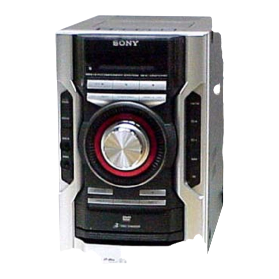
(Photo: HCD-GNZ444D)
Model Name Using Similar Mechanism
DVD
Section
Optical Pick-up Name
Tape Deck Model Name Using Similar Mechanism
Section
Tape Transport Mechanism Type
SPECIFICATIONS
Q Q
3
6 7
1 3
1 5
SUBWOOFER OUT (HCD-GNZ444D
only)
Power consumption:
190 W
Dimensions (w/h/d):
Approx. 200 × 306 × 410 mm
Mass:
Approx. 8.0 kg
Disc player section
System
Compact disc and digital audio and
video system
Laser
Semiconductor laser (DVD:
λ=650 nm, CD: λ=790 nm)
Emission duration: continuous
Frequency response
DVD (PCM 48 kHz): 2 Hz – 22 kHz
(±1dB)
CD: 2 Hz – 20 kHz (±0.5 dB)
Video color system format
NTSC and PAL
Tape deck section
Recording system: 4-track 2-channel, stereo
co
.
9 4
2 8
E Model
NEW
KHM-313CAB
HCD-EC55/EC77
CS-21SC-901TP
0 5
8
2 9
9 4
2 8
– Continued on next page –
m
DVD DECK RECEIVER
9 9
9 9
Advertisement
Table of Contents

Related Manuals for Sony HCD-GNZ333D


Summary of Contents for Sony HCD-GNZ333D
- Page 1 HCD-GNZ333D/GNZ444D 3 7 63 1515 0 SERVICE MANUAL E Model Ver. 1.4 2008.09 • HCD-GNZ333D/GNZ444D are the tuner, deck, DVD and amplifier section in MHC-GNZ333D/GNZ333DL/GNZ444D. (Photo: HCD-GNZ444D) Model Name Using Similar Mechanism Section Optical Pick-up Name KHM-313CAB Tape Deck Model Name Using Similar Mechanism...
- Page 2 COMPONENTS IDENTIFIED BY MARK 0 OR DOTTED LINE WITH MARK 0 ON THE SCHEMATIC DIAGRAMS AND IN THE PARTS LIST ARE CRITICAL TO SAFE OPERATION. REPLACE THESE COMPONENTS WITH SONY PARTS WHOSE PART NUMBERS APPEAR AS SHOWN IN THIS MANUAL OR IN SUPPLEMENTS PUBLISHED BY SONY.
- Page 3 HCD-GNZ333D/GNZ444D Ver. 1.2 3 7 63 1515 0 Notes on chip component replacement NOTES ON LASER DIODE EMISSION CHECK • Never reuse a disconnected chip component. The laser beam on this model is concentrated so as to be focused on •...
- Page 4 HCD-GNZ333D/GNZ444D 3 7 63 1515 0 MODEL IDENTIFICATION • Abbreviation : 240 V AC area in E model – BACK PANEL – E12 : 220-240 V AC area in E model E13 : Russian model E15 : Iran model...
-
Page 5: Table Of Contents
HCD-GNZ333D/GNZ444D 3 7 63 1515 0 TABLE OF CONTENTS SERVICING NOTES 7-4. Block Diagram – Display Section – ........ 34 ..........6 7-5. Printed Wiring Boards – Main Section – ......36 7-6. Schematic Diagram – Main Section (1/3) – ....37 GENERAL 7-7. -
Page 6: Servicing Notes
HCD-GNZ333D/GNZ444D SECTION 1 SERVICING NOTES 3 7 63 1515 0 1. CDM SERVICE POSITION CDM mechanism block DMB16 board J-2501-077-A (1.25m/13P/300L) L 13942296513 2. OPENING THE CD TRAY MANUAL 1 Turn the bottom rib (not the gear) with a flathead screwdriver in the direction of arrow A, with the lever pushed up, draw out the door (CD) by the hand. - Page 7 HCD-GNZ333D/GNZ444D 3 7 63 1515 0 3. NOTE FOR HANDLING THE BU Perform solder bridging to prevent damage by electrostatic discharge when handling the BU as a single unit. L 13942296513 4. ARRANGEMENT OF THE CORD cordes are fixed u163 http://www.xiaoyu163.com...
-
Page 8: General
HCD-GNZ333D/GNZ444D SECTION 2 This section is extracted from instruction manual. GENERAL 3 7 63 1515 0 L 13942296513 u163 http://www.xiaoyu163.com... - Page 9 HCD-GNZ333D/GNZ444D 3 7 63 1515 0 L 13942296513 u163 http://www.xiaoyu163.com...
- Page 10 HCD-GNZ333D/GNZ444D 3 7 63 1515 0 L 13942296513 u163 http://www.xiaoyu163.com...
- Page 11 HCD-GNZ333D/GNZ444D 3 7 63 1515 0 L 13942296513 u163 http://www.xiaoyu163.com...
- Page 12 HCD-GNZ333D/GNZ444D 3 7 63 1515 0 L 13942296513 u163 http://www.xiaoyu163.com...
- Page 13 HCD-GNZ333D/GNZ444D 3 7 63 1515 0 L 13942296513 u163 http://www.xiaoyu163.com...
- Page 14 HCD-GNZ333D/GNZ444D 3 7 63 1515 0 L 13942296513 u163 http://www.xiaoyu163.com...
-
Page 15: Disassembly
HCD-GNZ333D/GNZ444D SECTION 3 DISASSEMBLY 3 7 63 1515 0 Note: Disassemble the unit in the order as shown below. 3-1. SIDE PANEL (R), SIDE PANEL (L) (Page 16) 3-2. TOP PANEL SECTION (Page 16) 3-3. DOOR (CD) 3-6. DC FAN 3-5. -
Page 16: Side Panel (R), Side Panel (L)
HCD-GNZ333D/GNZ444D 3 7 63 1515 0 Note: Follow the disassembly procedure in the numerical order given. 3-1. SIDE PANEL (R), SIDE PANEL (L) 7 two screws 8 three screws (case 3 TP2) (+BVTP 3 × 10) 3 four screws 5 side panel (R) (+BVTP 3 ×... -
Page 17: Door (Cd)
HCD-GNZ333D/GNZ444D 3 7 63 1515 0 3-3. DOOR (CD) 4 door (CD) 3 Turn the bottom rib (not the gear) with a flathead screwdriver in the direction of arrow A, with the lever pushed up, draw out the door (CD) by the hand. -
Page 18: Main Board
HCD-GNZ333D/GNZ444D 3 7 63 1515 0 3-5. MAIN BOARD 2 wire (flat type) (9 core) qs REG board (connector) 4 tuner (FM/AM) (TN001) qj CN105 (3P) 3 two screws qa screw (+BVTP 2.6 × 8) (+BVTP 3 × 10) -
Page 19: Rear Panel
HCD-GNZ333D/GNZ444D 3 7 63 1515 0 3-7. REAR PANEL 5 rear panel section 1 cord bushing (2104) 2 two screws (+BVTP 3 × 10) 3 two screws (+BVTP 3 × 10) 4 two screws (+BVTP 3 × 10) L 13942296513 3-8. -
Page 20: Pt Board
HCD-GNZ333D/GNZ444D 3 7 63 1515 0 3-9. PT BOARD 2 two screws (+BVTT 4 × 6) 1 two screws (+BVTT 4 × 6) 3 PT board L 13942296513 3-10. COVER (CDM) 3 screw (+BV 3 (3-CR)) 4 FFC HOLD board... -
Page 21: Cd Mechanism Section
HCD-GNZ333D/GNZ444D 3 7 63 1515 0 3-11. CD MECHANISM SECTION 6 two screws 5 two screws (+BV 3 (3-CR)) (+BV 3 (3-CR)) 0 CD mechanism section 3 bracket (PT) 9 bracket (CDM) 2 two screws (+BVTP 3 × 10) 8 two screws (+BVTP 3 ×... -
Page 22: Belt (Dlm3A)
HCD-GNZ333D/GNZ444D 3 7 63 1515 0 3-13. BELT (DLM3A) 1 two screws 2 two screws 3 cover 4 belt (DLM3A) 5 belt (DLM3A) L 13942296513 3-14. OPTICAL PICK-UP 2 floating screw (+PTPWHM 2.6) 3 sheet (bottom) qs insulator 1 floating screw 7 two screws (+PTPWHM 2.6) -
Page 23: Mechanism Deck
HCD-GNZ333D/GNZ444D 3 7 63 1515 0 3-15. MECHANISM DECK 2 four screws (+BVTP 2.6 × 8 ) 1 Open the cassette box. 5 connector (CN501) 6 DECK board 7 mechanical deck 3 two screws (+BVTP 3 × 6 ) -
Page 24: Test Mode
HCD-GNZ333D/GNZ444D SECTION 4 TEST MODE 3 7 63 1515 0 [PANEL TEST MODE] [DVD SHIP MODE] • This mode is used to check the LCD display, LEDs, keys, • This mode can run the DVD sled motor optionally. Use this VOLUME jog and OPERATION DIAL jog, model, mode, for instance, when cleaning the optical pick-up. - Page 25 HCD-GNZ333D/GNZ444D Ver. 1.1 3 7 63 1515 0 [DVD SHIP AND COLD RESET] • Procedure to enter to DVD Service Mode: Procedure: 1. Press button to turn on the system. 1. Press the button to turn the power on.
- Page 26 HCD-GNZ333D/GNZ444D Ver. 1.1 3 7 63 1515 0 3. Select “6. Iop:” by pressing [6] button on the remote • Error Code commander. 4. Wait until a hexadecimal number appears in the on-screen Example of Error code display as below: 1.
- Page 27 HCD-GNZ333D/GNZ444D Ver. 1.1 3 7 63 1515 0 To clear the Laser Hour To return to the Top Menu of Remocon Diagnosis Menu Press [DISPLAY] button and then press [CLEAR] button. The data Press [0] button on the remote commander.
-
Page 28: Mechanical Adjustments
HCD-GNZ333D/GNZ444D SECTION 5 SECTION 6 MECHANICAL ADJUSTMENTS ELECTRICAL ADJUSTMENTS 3 7 63 1515 0 • Precaution DECK SECTION 0 dB=0.775 V 1. Clean the following parts with a denatured-alcohol-moistened swab : 1. Demagnetize the record/playback head with a head... - Page 29 HCD-GNZ333D/GNZ444D 3 7 63 1515 0 Adjustment Location: Record/Playback/Erase Head TUNER SECTION [FM TUNE LEVEL CHECK] signal generator OUTPUT (75 Ω ) Procedure: 1. Turn on the set. 2. Input the following signal from signal generator to FM antenna input directly.
- Page 30 HCD-GNZ333D/GNZ444D Ver. 1.1 3 7 63 1515 0 Checking Location: DMB16 board (Side A) DVD SECTION DMB16 BOARD When the optical pick-up assy is replaced, perform the “Execute CN105 pin 3 (GND) (SIDE A) CN105 pin 6 (RFMON) IOP Measurement”.
-
Page 31: Diagrams
HCD-GNZ333D/GNZ444D SECTION 7 3 7 6 3 1 5 1 5 0 DIAGRAMS 7-1. BLOCK DIAGRAM – RF/SERVO Section – CN105 RFMON TEST PIN V2REFO V2REFO DVDRFIP DVDA DVDB DETECTOR DVDC DVDD 8 NA 9 NB CD/DVD RF AMP,... -
Page 32: Block Diagram - Video Section
HCD-GNZ333D/GNZ444D 3 7 6 3 1 5 1 5 0 7-2. BLOCK DIAGRAM – VIDEO Section – VIDEO OUT BUFFER IC701 J701 4 IN YUV3 VIDEO 1 PS OPTICAL SPDIF TRANSMITTER DIGITAL IC555 D/A CONVERTER IC301 VIDEO MUTE MAIN... -
Page 33: Block Diagram - Main Section
HCD-GNZ333D/GNZ444D 3 7 6 3 1 5 1 5 0 7-3. BLOCK DIAGRAM – MAIN Section – RV261 MIC AMP LEVEL AMP-ON IC261 R-CH HP-DETECT J261 –IN J252 PHONES INPUT FUNCTION MIC MUTE CONTROL Q261 IC101 MIC MIX IC103 BASS BOOST –IN... -
Page 34: Block Diagram - Display Section
HCD-GNZ333D/GNZ444D 3 7 6 3 1 5 1 5 0 7-4. BLOCK DIAGRAM – DISPLAY Section – SYSTEM CONTROL LCD DISPLAY DRIVER IC401 (3/3) IC301 KEY1 FUNCTION KEY 67 I-KEY1 O-LCD-DATA 72 S351,352 O-LCD-CLK 70 SEG1 83 I-KEY-WAKE-UP O-LCD-CE 71 ND301 •... - Page 35 HCD-GNZ333D/GNZ444D 3 7 6 3 1 5 1 5 0 • Note for Printed Wiring Boards and Schematic Diagrams • Circuit Boards Location Note on Printed Wiring Board: Note on Schematic Diagram: • X : parts extracted from the component side.
-
Page 36: Printed Wiring Boards - Main Section
HCD-GNZ333D/GNZ444D • See page 35 for Circuit Boards Location. 7-5. PRINTED WIRING BOARDS – MAIN Section – : Uses unleaded solder. 3 7 6 3 1 5 1 5 0 AMP BOARD MAIN BOARD W751 (Page 48) TN001 TUNER UNIT... -
Page 37: Schematic Diagram - Main Section (1/3)
HCD-GNZ333D/GNZ444D • See page 58 for Waveforms. • See page 61 for IC Block Diagrams. 7-6. SCHEMATIC DIAGRAM – MAIN Section (1/3) – 3 7 6 3 1 5 1 5 0 MAIN BOARD (1/3) CN104 CN102 R049 PB-L... -
Page 38: Schematic Diagram - Main Section (2/3)
HCD-GNZ333D/GNZ444D 3 7 6 3 1 5 1 5 0 7-7. SCHEMATIC DIAGRAM – MAIN Section (2/3) – (Page 37) (Page 37) MAIN BOARD (1/3) MAIN BOARD (1/3) REG BOARD MAIN IC801 IC553 IC552 IC554 +9V REG BOARD C557... -
Page 39: Schematic Diagram - Main Section (3/3)
HCD-GNZ333D/GNZ444D • See page 58 for Waveforms. • See page 62 for IC Block Diagram. 3 7 6 3 1 5 1 5 0 • See page 63 for IC Pin Description of IC401. 7-8. SCHEMATIC DIAGRAM – MAIN Section (3/3) –... -
Page 40: Printed Wiring Board - Dmb16 Section (1/2)
HCD-GNZ333D/GNZ444D 3 7 6 3 1 5 1 5 0 • See page 35 for Circuit Boards Location. 7-9. PRINTED WIRING BOARD – DMB16 Section (1/2) – : Uses unleaded solder. DMB16 BOARD (SIDE A) PH,SP,TH MODELS C109 R212... -
Page 41: Printed Wiring Board - Dmb16 Section (2/2)
HCD-GNZ333D/GNZ444D Ver. 1.2 3 7 6 3 1 5 1 5 0 When IC103 on the DMB16 board are damaged, exchange the • See page 35 for Circuit Boards Location. 7-10. PRINTED WIRING BOARD – DMB16 Section (2/2) –... -
Page 42: Schematic Diagram - Dmb16 Section (1/6)
HCD-GNZ333D/GNZ444D 3 7 6 3 1 5 1 5 0 7-11. SCHEMATIC DIAGRAM – DMB16 Section (1/6) – DMB16 DMB16 BOARD (1/6) (Page 43) SW+5V BOARD (2/6) DMB16 (Page 44) SW+5V BOARD (3/6) DMB16 (Page 46) SW+5V BOARD CN401... -
Page 43: Schematic Diagram - Dmb16 Section (2/6)
HCD-GNZ333D/GNZ444D 3 7 6 3 1 5 1 5 0 • See page 58 for IC Block Diagrams. 7-12. SCHEMATIC DIAGRAM – DMB16 Section (2/6) – DMB16 BOARD (2/6) R3781 R3783 R3508 100 1.5k 3.9k ART- SCORE DMB16 R3507 100... -
Page 44: Schematic Diagram - Dmb16 Section (3/6)
HCD-GNZ333D/GNZ444D • See page 58 for IC Block Diagram. 7-13. SCHEMATIC DIAGRAM – DMB16 Section (3/6) – 3 7 6 3 1 5 1 5 0 DMB16 BOARD (3/6) DMB16 (Page 47) BOARD RF+3.3V RF+3.3V (6/6) DMB16 (Page 42) -
Page 45: Schematic Diagram - Dmb16 Section (4/6)
HCD-GNZ333D/GNZ444D • See page 58 for Waveforms. • See page 65 for IC Pin Description of IC102. 7-14. SCHEMATIC DIAGRAM – DMB16 Section (4/6) – 3 7 6 3 1 5 1 5 0 (Page 43) (Page 43) (Page 47) (Page 46) -
Page 46: Schematic Diagram - Dmb16 Section (5/6)
HCD-GNZ333D/GNZ444D Ver. 1.2 3 7 6 3 1 5 1 5 0 When IC103 on the DMB16 board are damaged, exchange the • See page 58 for IC Block Diagrams. 7-15. SCHEMATIC DIAGRAM – DMB16 Section (5/6) – new DMB16 board for the DMB16 board which IC damaged. -
Page 47: Schematic Diagram - Dmb16 Section (6/6)
HCD-GNZ333D/GNZ444D 3 7 6 3 1 5 1 5 0 7-16. SCHEMATIC DIAGRAM – DMB16 Section (6/6) – DMB16 BOARD (6/6) (Page 44) REG01 DMB16 BOARD REG02 (3/6) R231 0.5% FCS- FCS- R234 FCS+ DMB16 FCS+ DMB16 TRK+ BOARD... -
Page 48: Printed Wiring Board - Amp Section
HCD-GNZ333D/GNZ444D 3 7 6 3 1 5 1 5 0 • See page 35 for Circuit Boards Location. 7-17. PRINTED WIRING BOARD – AMP Section – : Uses unleaded solder. AMP BOARD R765 IC751 R761 C774 R788 C760 R794... -
Page 49: Schematic Diagram - Amp Section
HCD-GNZ333D/GNZ444D 3 7 6 3 1 5 1 5 0 • See page 60 for IC Block Diagram. 7-18. SCHEMATIC DIAGRAM – AMP Section – AMP BOARD IC B/D IC751 STK433-100-M-E IC751 POWER AMP R783 R781 R775 2.2k -0.4... -
Page 50: Printed Wiring Board - Deck Section
HCD-GNZ333D/GNZ444D 3 7 6 3 1 5 1 5 0 • See page 35 for Circuit Boards Location. 7-19. PRINTED WIRING BOARD – DECK Section – : Uses unleaded solder. DECK BOARD R527 C531 C525 R529 C529 C527 R525... -
Page 51: Schematic Diagram - Deck Section
HCD-GNZ333D/GNZ444D 3 7 6 3 1 5 1 5 0 • See page 58 for Waveform. 7-20. SCHEMATIC DIAGRAM – DECK Section – DECK BOARD C515 R509 R543 C545 R513 R515 100k R503 2.2k R545 C509 C513 S501 (REC/PB) -
Page 52: Printed Wiring Boards - Mic/Jack Section
HCD-GNZ333D/GNZ444D 3 7 6 3 1 5 1 5 0 • See page 35 for Circuit Boards Location. 7-21. PRINTED WIRING BOARDS – MIC/JACK Section – : Uses unleaded solder. J261 RV261 MIC BOARD MIC LEVEL R283 R277 R278... -
Page 53: Schematic Diagram - Mic/Jack Section
HCD-GNZ333D/GNZ444D 3 7 6 3 1 5 1 5 0 7-22. SCHEMATIC DIAGRAM – MIC/JACK Section – MIC BOARD R274 W262 MAIN MIC_SW BOARD (1/3) MIC_OUT CN103 C277 R275 A_GND (Page 37) R284 2.2k R282 100k C278 IC261 MIC AMP... -
Page 54: Printed Wiring Boards - Panel Section
HCD-GNZ333D/GNZ444D 3 7 6 3 1 5 1 5 0 • See page 35 for Circuit Boards Location. 7-23. PRINTED WIRING BOARDS – PANEL Section – : Uses unleaded solder. PANEL BOARD D303 IC302 (LCD BACK LIGHT) Q301 ND301... -
Page 55: Schematic Diagram - Panel Section
HCD-GNZ333D/GNZ444D 3 7 6 3 1 5 1 5 0 • See page 62 for IC Block Diagram. 7-24. SCHEMATIC DIAGRAM – PANEL Section – PANEL BOARD IC302 NJL24H400A IC302 REMOTE CONTROL RECEIVER ND301 LIQUID CRYSTAL DISPLAY PANEL R310... -
Page 56: Printed Wiring Board - Power Section
HCD-GNZ333D/GNZ444D 3 7 6 3 1 5 1 5 0 • See page 35 for Circuit Boards Location. 7-25. PRINTED WIRING BOARD – POWER Section – : Uses unleaded solder. AC IN PT BOARD EXCEPT E13 MODEL JW998 RY002... -
Page 57: Schematic Diagram - Power Section
HCD-GNZ333D/GNZ444D 3 7 6 3 1 5 1 5 0 7-26. SCHEMATIC DIAGRAM – POWER Section – PT BOARD D004 RY002 1SS133T-77 T002 POWER TRANSFORMER (SUB) EXCEPT EA MODEL EXCEPT E3 MODEL S001 VOLTAGE JW004 SELECTOR 120V JW009 D003... - Page 58 HCD-GNZ333D/GNZ444D 3 7 6 3 1 5 1 5 0 • Waveforms • IC Block Diagrams IC301 AK4358VQ-L (DMB16 Board (2/6)) – DMB16 Board – – MAIN Board – – DECK Board – (FL) IC701 2 (OUT) (DVD PLAY)
- Page 59 HCD-GNZ333D/GNZ444D 3 7 63 1515 0 IC101 MX29LV320CBTC70-CBA4-0701CE (DMB16 Board (5/6)) IC101 MX29LV320CBTC70-CBA4-0701GA (DMB16 Board (5/6)) BYTE DQ15/A–1 CONTROL WRITE INPUT PROGRAM/ERASE STATE LOGIC HIGH VOLTAGE DQ14 MACHINE (WSM) DQ13 DQ12 FLASH X–DECODER ADDRESS RESET ARRAY STATE ARRAY LATCH...
- Page 60 HCD-GNZ333D/GNZ444D 3 7 63 1515 0 IC106 NJM2387ADL3(TE2) (DMB16 Board (5/6)) CURRENT LIMIT OVERVOLTAGE THERMAL PROTECTION PROTECTION BANDGAP REFERENCE CONTROL VOUT VADJ L 13942296513 IC751 STK433-100-M-E (AMP Board) Pre Driver Pre Driver (CH1) (CH2) Bias Circuit 1 2 3...
- Page 61 HCD-GNZ333D/GNZ444D 3 7 63 1515 0 IC101 R2S15904SP (MAIN Board (1/3)) TUNER-R CD-R INPUT AUDIO-R SELECTOR L-OUT TAPE-R MUTE R-OUT TAPE-L A-GND MODE AUDIO-L SELECTOR INPUT SELECTOR TUNER-L CD-L INPUT GAIN CONTROL MUTE OUT-L DATA 0 - +12dB /2dB step...
- Page 62 HCD-GNZ333D/GNZ444D 3 7 63 1515 0 IC402 RST3429UL (MAIN Board (3/3)) Vref IC301 LC7827E-E (PANEL Board) 54 53 52 51 L 13942296513 VLCD1 VLCD2 COMMON DRIVER CLOCK GENERATOR SEG48 SEG12 SEG11 SEG1 1 O-BACKLIGHT-LED ADDRESS DETECTOR u163 http://www.xiaoyu163.com...
- Page 63 HCD-GNZ333D/GNZ444D 3 7 63 1515 0 • IC Pin Descriptions IC401 µPD78F1164GF(S)-301-GAS-AX (SYSTEM CONTROL) (MAIN BOARD (3/3)) Pin No. Pin Name Pin Description 1 to 9 — Not used I-AC-CUT AC off detection signal input 11, 12 — Not used...
- Page 64 HCD-GNZ333D/GNZ444D 3 7 63 1515 0 Pin No. Pin Name Pin Description I-KEY2 Key signal input (A/D input) I-KEY1 Key signal input (A/D input) O-LED-STBY Standby-LED drive signal output O-LCD-INH Inhibit signal output to LCD Driver O-LCG-CLK Serial clock signal output to LCD Driver...
- Page 65 HCD-GNZ333D/GNZ444D 3 7 63 1515 0 IC102 CXD9849R (CD/DVD RF AMP, FOCUS/TRACKING ERROR AMP, DVD SYSTEM PROCESSOR, DIGITAL SERVO PROCESSOR) (DMB16 BOARD (4/6)) Pin No. Pin Name Pin Description AGND — Ground DVDA AC coupled input path A DVDB...
- Page 66 HCD-GNZ333D/GNZ444D 3 7 63 1515 0 Pin No. Pin Name Pin Description SPFG Motor Hall sensor signal input DSEL Select signal output Not used in this set. (Open) WIDE Wide signal output Not used in this set. Volume control signal output...
- Page 67 HCD-GNZ333D/GNZ444D 3 7 63 1515 0 Pin No. Pin Name Pin Description DQMO DQM0 signal output to SD-RAM MREQ DQM signal input Data bus 7 from SD-RAM DVSS — Ground 117, 118 RD 6, 5 Data bus 6, 5 from SD-RAM DVSS —...
- Page 68 HCD-GNZ333D/GNZ444D 3 7 63 1515 0 Pin No. Pin Name Pin Description OCSW SEN signal input from System Controller/OCSW signal input Not used. (Open) — Not used in this set. (Open) CKSW CKSW signal input Not used in this set. (Open) —...
- Page 69 HCD-GNZ333D/GNZ444D 3 7 63 1515 0 Pin No. Pin Name Pin Description RFVDD18 — Power Supply (+1.8 V) XTALO Oscillator signal output (27 MHz) XTALI Oscillator signal input (27 MHz) JITFO RF jitter meter output JITFN Negative input of operation amplifier for RF jigger meter PLLVSS —...
-
Page 70: Exploded Views
HCD-GNZ333D/GNZ444D SECTION 8 EXPLODED VIEWS 3 7 63 1515 0 NOTE: The components identified by mark • The mechanical parts with no reference • Abbreviation 0 or dotted line with mark 0 are number in the exploded views are not supplied. -
Page 71: Front Panel Section
HCD-GNZ333D/GNZ444D 3 7 63 1515 0 8-2. FRONT PANEL SECTION not supplied not supplied (KEY LEFT board) (JACK HOLD board) not supplied not supplied (JACK board) ND301 not supplied (KEY RIGHT board) not supplied L 13942296513 not supplied not supplied... -
Page 72: Main Board Section
HCD-GNZ333D/GNZ444D 3 7 63 1515 0 8-3. MAIN BOARD SECTION TN001 not supplied (F HOLD B board) not supplied not supplied (FFC HOLD board) (F HOLD A board) FC001 IC801 not supplied L 13942296513 (REG board) not supplied not supplied Ref. -
Page 73: Rear Panel Section
HCD-GNZ333D/GNZ444D 3 7 63 1515 0 8-4. REAR PANEL SECTION T001 FC002 not supplied not supplied (PT board) not supplied (WIRE BIND board) not supplied not supplied F004 (AMP board) F003 F002 F001 not supplied (HOLD A board) not supplied... -
Page 74: Chassis Section
HCD-GNZ333D/GNZ444D Ver. 1.2 3 7 63 1515 0 8-5. CHASSIS SECTION CD mechanism deck section not supplied not supplied not supplied not supplied not supplied L 13942296513 not supplied (WIRE PROTECT board) not supplied Ref. No. Part No. Description Remark Ref. -
Page 75: Top Panel Section
HCD-GNZ333D/GNZ444D 3 7 63 1515 0 8-6. TOP PANEL SECTION not supplied not supplied not supplied not supplied L 13942296513 not supplied Ref. No. Part No. Description Remark Ref. No. Part No. Description Remark 2-649-131-21 BOX, CASSETTE A-1223-698-A DECK BOARD, COMPLETE... -
Page 76: Dvd Mechanism Deck Section
HCD-GNZ333D/GNZ444D 3 7 63 1515 0 8-7. DVD MECHANISM DECK SECTION supplied not supplied not supplied supplied supplied not supplied L 13942296513 not supplied not supplied Ref. No. Part No. Description Remark Ref. No. Part No. Description Remark u163... -
Page 77: Electrical Parts List
HCD-GNZ333D/GNZ444D SECTION 9 ELECTRICAL PARTS LIST 3 7 63 1515 0 NOTE: When indicating parts by reference • Due to standardization, replacements in the • SEMICONDUCTORS In each case, u : µ, for example: number, please include the board. - Page 78 HCD-GNZ333D/GNZ444D DECK 3 7 63 1515 0 Ref. No. Part No. Description Remark Ref. No. Part No. Description Remark A-1223-698-A DECK BOARD, COMPLETE < JUMPER RESISTOR > ********************* JR501 1-216-864-11 SHORT CHIP < CAPACITOR > JR502 1-216-864-11 SHORT CHIP...
- Page 79 HCD-GNZ333D/GNZ444D Ver. 1.2 DECK DMB16 3 7 63 1515 0 Ref. No. Part No. Description Remark Ref. No. Part No. Description Remark R546 1-216-817-11 METAL CHIP 1/10W C156 1-162-970-11 CERAMIC CHIP 0.01uF C158 1-162-970-11 CERAMIC CHIP 0.01uF < SWITCH >...
- Page 80 HCD-GNZ333D/GNZ444D Ver. 1.2 DMB16 3 7 63 1515 0 Ref. No. Part No. Description Remark Ref. No. Part No. Description Remark C403 1-126-786-11 ELECT 47uF FB1502 1-400-244-11 BEAD, FERRITE (CHIP) (1608) C3701 1-107-826-11 CERAMIC CHIP 0.1uF FB3501 1-400-244-11 BEAD, FERRITE (CHIP) (1608)
- Page 81 HCD-GNZ333D/GNZ444D DMB16 3 7 63 1515 0 Ref. No. Part No. Description Remark Ref. No. Part No. Description Remark R127 1-216-809-11 METAL CHIP 1/10W R1110 1-216-826-11 METAL CHIP 2.7K 1/10W R136 1-216-835-11 METAL CHIP 1/10W R1123 1-216-864-11 SHORT CHIP...
- Page 82 HCD-GNZ333D/GNZ444D DMB16 JACK KEY CD KEY LEFT KEY RIGHT 3 7 63 1515 0 Ref. No. Part No. Description Remark Ref. No. Part No. Description Remark R3726 1-216-821-11 METAL CHIP 1/10W < JACK > R3727 1-216-821-11 METAL CHIP 1/10W...
- Page 83 HCD-GNZ333D/GNZ444D MAIN 3 7 63 1515 0 Ref. No. Part No. Description Remark Ref. No. Part No. Description Remark A-1223-667-A MAIN BOARD, COMPLETE (GNZ333D:EA) C129 1-165-908-11 CERAMIC CHIP A-1223-668-A MAIN BOARD, COMPLETE (GNZ333D:PH,SP,TH) C130 1-165-908-11 CERAMIC CHIP A-1223-669-A MAIN BOARD, COMPLETE (GNZ333D:E3,E15)
- Page 84 HCD-GNZ333D/GNZ444D Ver. 1.4 MAIN 3 7 63 1515 0 Ref. No. Part No. Description Remark Ref. No. Part No. Description Remark C554 1-126-961-11 ELECT 2.2uF D018 8-719-063-79 DIODE 1N4002B C555 1-126-947-11 ELECT 47uF D019 8-719-063-79 DIODE 1N4002B C556 1-126-947-11 ELECT...
- Page 85 HCD-GNZ333D/GNZ444D MAIN 3 7 63 1515 0 Ref. No. Part No. Description Remark Ref. No. Part No. Description Remark IC701 6-600-495-01 IC MM1671XNRE Q101 8-729-120-28 TRANSISTOR 2SC1623-L5L6 Q102 8-729-120-28 TRANSISTOR 2SC1623-L5L6 < JACK > Q103 8-729-120-28 TRANSISTOR 2SC1623-L5L6 Q104...
- Page 86 HCD-GNZ333D/GNZ444D MAIN 3 7 63 1515 0 Ref. No. Part No. Description Remark Ref. No. Part No. Description Remark R055 1-216-826-11 METAL CHIP 2.7K 1/10W R136 1-216-838-11 METAL CHIP 1/10W R056 1-216-825-11 METAL CHIP 2.2K 1/10W R137 1-216-841-11 METAL CHIP...
- Page 87 HCD-GNZ333D/GNZ444D MAIN 3 7 63 1515 0 Ref. No. Part No. Description Remark Ref. No. Part No. Description Remark R192 1-216-841-11 METAL CHIP 1/10W R426 1-216-829-11 METAL CHIP 4.7K 1/10W R193 1-216-846-11 METAL CHIP 120K 1/10W (E3,E12,E15,EA) R194 1-216-846-11 METAL CHIP...
- Page 88 HCD-GNZ333D/GNZ444D MAIN 3 7 63 1515 0 Ref. No. Part No. Description Remark Ref. No. Part No. Description Remark R484 1-216-837-11 METAL CHIP 1/10W R601 1-249-403-11 CARBON 1/4W R485 1-216-837-11 METAL CHIP 1/10W R602 1-249-403-11 CARBON 1/4W R486 1-216-837-11 METAL CHIP...
- Page 89 HCD-GNZ333D/GNZ444D PANEL 3 7 63 1515 0 Ref. No. Part No. Description Remark Ref. No. Part No. Description Remark C281 1-162-953-11 CERAMIC CHIP 100PF C304 1-165-176-11 CERAMIC CHIP 0.047uF C282 1-162-927-11 CERAMIC CHIP 100PF C305 1-162-964-11 CERAMIC CHIP 0.001uF...
- Page 90 HCD-GNZ333D/GNZ444D 3 7 63 1515 0 Ref. No. Part No. Description Remark Ref. No. Part No. Description Remark PT BOARD MISCELLANEOUS ********* *************** 1-533-217-41 HOLDER, FUSE 1-831-755-21 CABLE, FLEXIBLE FLAT (5 CORE) < CONNECTOR > 1-828-895-51 WIRE (FLAT TYPE) (15 CORE)
- Page 91 HCD-GNZ333D/GNZ444D 3 7 63 1515 0 MEMO L 13942296513 u163 http://www.xiaoyu163.com...
- Page 92 HCD-GNZ333D/GNZ444D 3 7 63 1515 0 REVISION HISTORY Clicking the version allows you to jump to the revised page. Also, clicking the version at the top of the revised page allows you to jump to the next revised page.