Yamaha RX-V1500 Service Manual
Av receiver/av amplifier
Hide thumbs
Also See for RX-V1500:
- Product catalog (44 pages) ,
- Owner's manual (104 pages) ,
- Owner's manual (700 pages)
Table of Contents
Advertisement
Quick Links
RX-V1500/DSP-AX1500
This manual has been provided for the use of authorized YAMAHA Retailers and their service personnel.
It has been assumed that basic service procedures inherent to the industry, and more specifically YAMAHA Products, are already
known and understood by the users, and have therefore not been restated.
WARNING:
IMPORTANT:
The data provided is believed to be accurate and applicable to the unit(s) indicated on the cover. The research, engineering, and
service departments of YAMAHA are continually striving to improve YAMAHA products. Modifications are, therefore, inevitable
and specifications are subject to change without notice or obligation to retrofit. Should any discrepancy appear to exist, please
contact the distributor's Service Division.
WARNING:
IMPORTANT:
I CONTENTS
To Service Personnel .......................................... 2
FRONT PANELS ........................................................ 3~4
Rear Panels .......................................................... 4~7
Remote Control ...................................................... 7
Specifications .................................................... 8~11
Internal View ......................................................... 12
..................................... 17~18
1 0 0 9 1 9
AV RECEIVER/AV AMPLIFIER
IMPORTANT NOTICE
Failure to follow appropriate service and safety procedures when servicing this product may result in personal
injury, destruction of expensive components, and failure of the product to perform as specified. For these reasons,
we advise all YAMAHA product owners that any service required should be performed by an authorized
YAMAHA Retailer or the appointed service representative.
The presentation or sale of this manual to any individual or firm does not constitute authorization, certification or
recognition of any applicable technical capabilities, or establish a principle-agent relationship of any form.
Static discharges can destroy expensive components. Discharge any static electricity your body may have
accumulated by grounding yourself to the ground buss in the unit (heavy gauge black wires connect to this buss).
Turn the unit OFF during disassembly and part replacement. Recheck all work before you apply power to the unit.
......... 13~16
19~43
SERVICE MANUAL
Display Data ..................................................... 46~47
Ic Data ................................................................. 48~57
Block Diagram ................................................. 58~59
Printed Circuit Board .................................. 60~74
Pin Connection Diagram .............................. 75~76
Schematic Diagram ........................................ 77~85
PARTS LIST ......................................................... 87~123
REMOTE CONTROL .......................................... 124~125
44~45
P.O.Box 1, Hamamatsu, Japan
'04.09
Advertisement
Table of Contents

Related Manuals for Yamaha RX-V1500


Summary of Contents for Yamaha RX-V1500
-
Page 1: Service Manual
This manual has been provided for the use of authorized YAMAHA Retailers and their service personnel. It has been assumed that basic service procedures inherent to the industry, and more specifically YAMAHA Products, are already known and understood by the users, and have therefore not been restated. -
Page 2: To Service Personnel
RX-V1500/DSP-AX1500 I TO SERVICE PERSONNEL AC LEAKAGE WALL EQUIPMENT TESTER OR 1. Critical Components Information OUTLET UNDER TEST EQUIVALENT Components having special characteristics are marked s and must be replaced with parts having specifications equal to those originally installed. 2. Leakage Current Measurement (For 120V Models Only) -
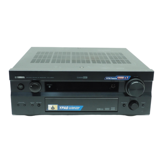
Page 3: Front Panels
I FRONT PANELS RX-V1500 (U, C, A models) RX-V1500 (R, T, K, L models) RX-V1500 (B, G models) -
Page 4: Rear Panels
RX-V1500/DSP-AX1500 DSP-AX1500 (J model) REAR PANELS RX-V1500 (U, C models) RX-V1500 (R model) - Page 5 RX-V1500/DSP-AX1500 RX-V1500 (T model) RX-V1500 (K model) RX-V1500 (A model)
- Page 6 RX-V1500/DSP-AX1500 RX-V1500 (B model) RX-V1500 (G model) RX-V1500 (L model)
-
Page 7: Remote Control
RX-V1500/DSP-AX1500 DSP-AX1500 (J model) I REMOTE CONTROL RX-V1500 (U, C, R, T, K, A, L models) RX-V1500 (B, G models) DSP-AX1500 (J models) -
Page 8: Specifications
RX-V1500/DSP-AX1500 Residual Noise (IHF-A network) I SPECIFICATIONS FRONT L/R SP OUT ..........150µV or less Channel Separation I Audio Section (STEREO) PHONO (Input shorted, 1 kHz/10 kHz) ...... 60dB or more/55dB or more Minimum RMS Output Power (Power Amp. Section) CD, etc. - Page 9 ..... 435 x 171 x 433.5 mm (17-1/8" x 6-3/4" x 17-1/16") Weight RX-V1500/DSP-AX1500 ......15.5 kg (34 lbs. 3 oz.) Finish RX-V1500 ......Gold color (R, T, K, L) models 7ch Stereo Parameter Unit Black color (U, C, R, A, G) models CT.
- Page 10 RX-V1500/DSP-AX1500...
- Page 11 RX-V1500/DSP-AX1500...
-
Page 12: Internal View
RX-V1500/DSP-AX1500 I INTERNAL VIEW 4 5 6 7 8 9 1 POWER (5) P.C.B. 2 POWER (4) P.C.B. (R, L models only) 3 MAIN (1) P.C.B. 4 POWER (7) P.C.B. (U, C, A, B, G models only) 5 MAIN (5) P.C.B. -
Page 13: Disassembly Procedures
RX-V1500/DSP-AX1500 I DISASSEMBLY PROCEDURES * The description below uses RX-V1500 (G model) as a representative model. (Remove parts in the order as numbered.) Disconnect the power cable from the AC outlet. 1. Removal of Top Cover a. Remove 2 screws (1), 4 screws (2) and 5 screws (3). - Page 14 RX-V1500/DSP-AX1500 5. Removal of VIDEO (2) P.C.B. a. Remove 1 screw (B). (Fig. 2) b. Remove CB554, CB555 and CB558. (Fig. 3) c. Remove the VIDEO (2) P.C.B. which is connected directly to the lower P.C.B. with connectors. (Fig. 2) VIDEO (2) P.C.B.
- Page 15 RX-V1500/DSP-AX1500 6. Removal of VIDEO (1) ~ (3), (5) ~ (8), FUNCTION, CONVERSION P.C.B.s and Tuner a. Remove 26 screws (C). (Fig. 4) b. Remove VIDEO (1) ~ (3), (5) ~ (8), FUNCTION, CONVERSION P.C.B.s and Tuner. (Fig. 5) When checking the P.C.B.: •...
- Page 16 RX-V1500/DSP-AX1500 7. Removal of Fan a. Remove 4 push rivets (D) and then remove the Cover. (Fig. 6) b. Remove 2 screws (E) and 2 screws (F). (Fig. 6) c. Remove the Fan together with the frame by lifting them up.
-
Page 17: Updating Firmware
RX-V1500/DSP-AX1500 I UPDATING FIRMWARE After replacing the IC512 on the FUNCTION P.C.B. with the service part (X4678A00), update the firmware according to the following procedure. Equipment required • PC with RS-232C serial port (OS: Windows98/2000/ Me/XP) • Firmware loading program (YAVBoot_V518.exe) •... - Page 18 RX-V1500/DSP-AX1500 2. After executing the firmware loading program, select the program type and port settings as follows: Program Type Select COM > SETTING Menu Port Setting Dialog 3. Turn on the power to the unit. 4. To connect the line, click the CONNECT button or the COM menu, then click the CONNECT.
- Page 19 RX-V1500/DSP-AX1500 I SELF DIAGNOSIS FUNCTION (DIAG) There are 18 DIAG menu items, each of which has sub- menu items. Listed in the table below are menu items and sub-menu items. No DIAG menu sub-menu DA601-YSS930 1. YSS 0dB 2. YSS FULL BIT BYPASS 1.
- Page 20 RX-V1500/DSP-AX1500 No DIAG menu sub-menu 12 AD DATA CHECK 1. DC/PS (protection) /FAN TEST 2. THM/FAN OUT 3. REC-OUT 4. IMP SW/POWER LIMIT 5. K0/K1 (panel key) 6. FAN DRIVE TEST: HIGH 7. FAN DRIVE TEST: MID 8. FAN DRIVE TEST: LOW 13 V CONV STATUS 1.
- Page 21 RX-V1500/DSP-AX1500 • Starting DIAG Press the “STANDBY/ON” key while simultaneously pressing those two keys of the main unit as indicated in the figure below. Keys of main unit Turn on the power while pressing these keys. • Starting DIAG in the protection cancel...
- Page 22 RX-V1500/DSP-AX1500 • Display provided when DIAG started When the monitor is connected, DIAGNOSTIC MENU appears on its screen as shown in the figure. (It remains on display until DIAG is cancelled.) The FL display of the main unit displays the protection function history data and the version (1 alphabet) and the DIAG menu [sub-menu (YSS 0dB) of DIAG menu No.1...
- Page 23 RX-V1500/DSP-AX1500 When there is a history of protection function due to abnormal voltage in the power supply section Version (1 alphabet) Voltage display in % Cause: The voltage in the power supply section is abnormal. Supplementary information: The abnormal voltage is displayed in % based on 5V as 100%.
- Page 24 RX-V1500/DSP-AX1500 • History of protection function When the protection function has worked, its history is stored in memory with a backup. Even if no abnormality is noted while servicing the unit, an abnormality which has occurred previously can be defined as long as the backup data has been stored.
- Page 25 RX-V1500/DSP-AX1500 • Functions in DIAG mode In addition to the DIAG menu items, functions as listed below are available. • Input selection, Multi channel input • Center/Surround/Surround Back/Sub-woofer level adjustment • Muting • Speaker relay A/B • Power on/off • Master volume * Functions related to the tuner and the set menu are not available.
- Page 26 RX-V1500/DSP-AX1500 • Details of DIAG menu With full-bit output specified in some modes, it is possible to execute 0dBFS output without head margin in each channel. 1. DA601-YSS930 This function is for YSS930 only. Main DSP of YSS930 is selected for FRONT output.
- Page 27 RX-V1500/DSP-AX1500 2. BYPASS ANALOG BYPASS Reference data INPUT: DVD ANALOG SUBWOOFER: 50Hz, Others: 1kHz PRE OUTPUT Input level Volume FRONT CENTER SURROUND SURROUND BACK SUBWOOFER - ∞ - ∞ - ∞ - ∞ Both ch, -20 dBm +6.5 dB -15.7 dBm...
- Page 28 RX-V1500/DSP-AX1500 3. RAM THROUGH Using the sub-menu, it is possible to select the full-bit output at 0dB output level. RAM 0dB Reference data INPUT: DVD ANALOG SUBWOOFER: 50Hz, Others: 1kHz PRE OUTPUT Input level Volume FRONT CENTER SURROUND SURROUND BACK SUBWOOFER Both ch, -20 dBm +6.5 dB...
- Page 29 RX-V1500/DSP-AX1500 4. PRO LOGIC / NEO6 PRO LOGIC I Reference data INPUT: DVD ANALOG SUBWOOFER: 50Hz, Others: 1kHz PRE OUTPUT Input level Volume FRONT CENTER SURROUND SURROUND BACK SUBWOOFER - ∞ - ∞ - ∞ - ∞ Each ch, -20 dBm +6.5 dB...
- Page 30 RX-V1500/DSP-AX1500 5. SPEAKERS SET The input signal is automatically identified in the order of dts → DOLBY DIGITAL → AAC→ PCM → Analog. There are seven sub-menu items as follows. The signals output from the DSP block are the same as 1.
- Page 31 RX-V1500/DSP-AX1500 6. EXTERNAL INPUT It is possible to select the 6ch/8ch input and 6_/8_ by using the SUB menu. 6CH_INPUT_6OHMS 6CH_INPUT_8OHMS 8CH_INPUT_6OHMS 8CH_INPUT_8OHMS Reference data INPUT: DVD ANALOG SUBWOOFER: 50Hz, Others: 1kHz PRE OUTPUT Sub-menu Input level Volume FRONT CENTER SURROUND SURROUND BACK SUBWOOFER - ∞...
- Page 32 RX-V1500/DSP-AX1500 8. EFFECT OFF / DISPLAY CHECK This program is used to check the FL display section. The display condition varies as shown below according to the sub-menu operation. The signals are processed using EFFECT OFF (The L/R signal is output using ANALOG MAIN BYPASS.)
- Page 33 RX-V1500/DSP-AX1500 9. MANUAL TEST The noise generator with a built-in DSP outputs the test noise through the channels specified by the sub-menu. The noise frequency for LFE is 35 to 250 Hz. Other than that, the center frequency is 800Hz.
- Page 34 RX-V1500/DSP-AX1500 10. RS-232C This menu is used to check transmission of the data and the flow port of the hardware. With the power turned off, short between pins No.2 (RxD) and No.3 (TxD), and between pins No.7 (RTS) and No.8 (CTS) of the RS-232C terminal. (Be sure to turn off the power when shorting the pins.)
- Page 35 RX-V1500/DSP-AX1500 11. FACTORY PRESET This menu is used to reserve and inhibit initialization of the back-up RAM. The signals are processed using EFFECT OFF. (The L/R signal is output using ANALOG MAIN BYPASS.) PRESET INHIBIT (Initialization inhibited) / RAM initialization is not executed. Select this sub-menu to protect the values set by the user.
- Page 36 RX-V1500/DSP-AX1500 12. AD DATA CHECK / FAN TEST This menu is used to display the A/D conversion value of the main CPU which detects panel keys of the main unit and protection functions in % using the sub-menu. During signal processing, the condition before execution is maintained.
- Page 37 RX-V1500/DSP-AX1500 IMP SW/POWER LIMIT (Impedance/power limiter detection) IMP: Not applied to this model. PL: Power limiter detection value The voltage value of pin No. 135 of IC520 is displayed, using 5V/256 as standard. Based on the input voltage value of pin No.135 of IC520, the output of pins No.6 (LC1) and No.7 (LC2) of...
- Page 38 RX-V1500/DSP-AX1500 FAN DRIVE TEST (For models so equipped) 13. V CONV STATUS The data received from the video conversion IC (TA1270) is displayed. LOW BYTE DATA The status information of TA1270 is displayed in the binary notation. HIGH BYTE DATA...
- Page 39 RX-V1500/DSP-AX1500 14. IF STATUS (Input function status) Using the sub-menu, the status data is displayed one after another in the hexadecimal notation. During signal processing, the status before execution of this menu is maintained. * Numeric values in the figure example are for reference.
- Page 40 RX-V1500/DSP-AX1500 <5th byte> Signal processing status information *2: With digital signals other than 32kHz, 44.1kHz and 48kHz, through processing method is used for reproducible signals. bit7 MUTE request bit3 – bit6 Red dts flashing bit2 Through & bypass (*2) bit5 6.1/EX processing...
- Page 41 RX-V1500/DSP-AX1500 15. DSP RAM CHECK This menu is used to self-diagnose whether or not the bus connection for the YSS930 and the external RAM is made properly. During signal processing, the status before execution of this menu is maintained. The address bus and the data bus are checked and the connection condition is displayed.
- Page 42 RX-V1500/DSP-AX1500 17. SOFT SW This menu is used to switch the function settings on P.C.B. through the software so as to activate the product. The protection function follows the P.C.B. settings. When connected to AC or in the maker preset state, the unit is initialized to the P.C.B.
- Page 43 RX-V1500/DSP-AX1500 18. MICROPROCESSOR INFORMATION The version, checksum and the port specified by the microprocessor are displayed. The signal is processed using EFFECT OFF. The checksum is obtained by adding the data at every 16 bits for each program area and expressing the result as a 4-figure hexadecimal data.
-
Page 44: Amp Adjustment
RX-V1500/DSP-AX1500 I AMP ADJUSTMENT Confirmation of Idling Current of Amp Unit • Right after power is turned on, confirm that the voltage across the terminals of R319 (Main Lch), R320 (Main Rch), R325 (Center), R326 (SURROUND Lch), R327 (SURROUND Rch), R321 (SURROUND BACK Lch), R322 (SURROUND BACK Rch) are between 0.1mV... - Page 45 RX-V1500/DSP-AX1500 MAIN (2) P. C. B. MAIN (3) P. C. B. POWER (3) P. C. B. MAIN (4) P. C. B.
-
Page 46: Display Data
RX-V1500/DSP-AX1500 I DISPLAY DATA G V901 : 17-BT-23GNK (WD507500) PATTERN AREA G PIN CONNECTION Pin No. Connection Pin No. Connection Note : 1) F1, F2 ..Filament 2) NP ..No pin 3) NC ..No connection 4) NX ..No extened Pin 5) 1G ~ 17G .. - Page 47 RX-V1500/DSP-AX1500 G ANODE CONNECTION 14G~2G – – – – – – – – – – – – – –...
- Page 48 RX-V1500/DSP-AX1500 I IC DATA IC509: LC89057W-VF4-E (DSP P.C.B) Digital Audio Interface Transceiver SDIN SLRCK SBCK RDATA XMODE RLRCK DGND DVDD LC89057W-VF4-E DVDD DGND TMCK/PIO0 RBCK TBCK/PIO1 RMCK TLRCK/PIO2 AGND TDATA/PIO3 AVDD TXO/PIOE *: Pull-down resistor internal RXOUT Microcontroller Cbit, Ubit...
- Page 49 RX-V1500/DSP-AX1500 IC509: LC89057W-VF4-E (DSP P.C.B) Digital Audio Interface Transceiver Name Function 1) Input/output I or O = -0.3 to 3.6V, Is = -0.3 to 5.5V 2) Pins 32 and 33 are latch address setting input pins when pin 41 = "L".
- Page 50 RX-V1500/DSP-AX1500 IC512: D601A002PYP180 (DSP P.C.B) Decoder Digital Signal Processors EMIF32 L2 Cache/ L1P Cache Memory Direct Mapped 4 Banks McASP1 4K Bytes Total 64K Bytes Total McASP0 (4-Way) C67x McBSP1 Control Instruction Fetch Registers McBSP0 Instruction Dispatch Control Instruction Decode...
- Page 51 RX-V1500/DSP-AX1500 IC512: D601A002PYP180 (DSP P.C.B) Decoder Name Function 12C0 clock 12C0 data 1.2V power supply 3.3V power supply Ground 1.2V power supply 3.3V power supply Ground Ground 1.2V power supply 1.2V power supply Ground 1.2V power supply Ground 3.3v power supply...
- Page 52 RX-V1500/DSP-AX1500 IC512: D601A002PYP180 (DSP P.C.B) Decoder Name Function For external memory, Address 17 For external memory, Address 19 For external memory, Address 20 For external memory area, Enable 0 For external memory area, Enable 1 1.2V power supply 1.2V power supply Ground 3.3V power supply...
- Page 53 RX-V1500/DSP-AX1500 IC512: D601A002PYP180 (DSP P.C.B) Decoder Name Function 1.2V power supply Ground General purpose I/O0 port 8 HPI data pin 8 McASP1 reception MCLK 3.3V power supply Ground General purpose I/O0 port 3 General purpose I/O0 port 9 General purpose I/O0 port 10...
- Page 54 RX-V1500/DSP-AX1500 IC516, 518: YSS930 (DSP P.C.B.) VDD2 RAMA11 RAMD9 RAMA12 RAMD8 RAMA13 RAMD7 RAMA14 RAMD6 RAMA15 RAMD5 RAMA16 RAMD4 RAMA17 RAMD3 VDD1 RAMD2 RAMD1 RAMD0 VDD1 IOPORT19 IOPORT18 SDWCK IOPORT17 SDBCK IOPORT16 SDI7 SDO7 SDI6 SDO6 SDI5 SDO5 SDI4 SDO4...
- Page 55 RX-V1500/DSP-AX1500 IC516, 518: YSS930 (DSP P.C.B.) IC516, 518: YSS930 (DSP P.C.B.) Name Function Name Function Digital ground terminal Data input/output terminal 14 for external memory Terminal for connecting crystal oscillator Data input/output terminal 15 for external memory Terminal for connecting crystal oscillator...
- Page 56 RX-V1500/DSP-AX1500 IC520 : M30805SGP (FUNCTION P.C.B) IC520 : M30805SGP (FUNCTION P.C.B) 16bit µ-COM (Main CPU) 16bit µ-COM (Main CPU) Pin Pin function Function Name Detail of function Backup P96/ANEX1/TxD4/SDA4/SRxD4 TxD4 TXDR 232C TX data / YDC TX data P95/ANEX0/CLK4 CLK4...
- Page 57 RX-V1500/DSP-AX1500 IC520 : M30805SGP (FUNCTION P.C.B) IC520 : M30805SGP (FUNCTION P.C.B) 16bit µ-COM (Main CPU) 16bit µ-COM (Main CPU) Pin Pin function Function Name Detail of function Backup Pin Pin function Function Name Detail of function Backup P53/BCLK/ALE/CLKout BCLK BCLK...
- Page 58 RX-V1500/DSP-AX1500 I BLOCK DIAGRAM (1/2) • See page 77~78 → SCHEMATIC DIAGRAM • See page 79~80 → SCHEMATIC DIAGRAM FUNCTION 39,40 IC502,506 SDO4 SDO3 Input Selector 125,126 SW920 TID0 38,39 REC 1,2 SDO5 136,137 IC529 32,33 IC519 SDO4 SW901-903 SW905-908,911...
- Page 59 RX-V1500/DSP-AX1500 I BLOCK DIAGRAM (2/2) • See page 84 → SCHEMATIC DIAGRAM • See page 82 → SCHEMATIC DIAGRAM IC703 MAIN Input Selector SOURCE VIDEO D246 IC607 IC601 2/2 Y/C Mix. Selector IC811 IC701 IC607 IC23 IC601 1/2 IC24 IC603...
- Page 60 RX-V1500/DSP-AX1500 I PRINTED CIRCUIT BOARD (Foil side) • Semiconductor Location Ref. No. Location D501 D502 D509 DSP P.C.B. (Side A) Lead Solder Used D512 D513 FUNCTION D515 OPERATION (3) FUNCTION D516 FUNCTION D518 POWER (3) D520 D521 IC501 IC502 IC503...
- Page 61 RX-V1500/DSP-AX1500 I PRINTED CIRCUIT BOARD (Foil side) • Semiconductor Location Ref. No. Location D510 D514 D517 DSP P.C.B. (Side B) Lead Free Solder Used D519 D524 D525 D528 D529 D530 J505 D531 D532 D533 D534 D535 D536 D537 D538 D539...
- Page 62 RX-V1500/DSP-AX1500 I PRINTED CIRCUIT BOARD (Foil side) FUNCTION P.C.B. (Side A) Lead Solder Used VIDEO (2) POWER (3) OPERATION (1) MAIN (1) (PLAY) OPERATION (2) MD/TAPE (REC) KEY1B +5M2 /RES BOOT (PLAY) CD-R (REC) HPMT /MIC +5M2 OPERATION (3) PHONO...
- Page 63 RX-V1500/DSP-AX1500 I PRINTED CIRCUIT BOARD (Foil side) FUNCTION P.C.B. (Side B) Lead Free Solder Used Circuit No. U, C T, K B, G • Semiconductor Location C513, 533, 561, 562, 564, 566, 568, Ref. No. Location Ref. No. Location Ref. No. Location Ref.
- Page 64 RX-V1500/DSP-AX1500 I PRINTED CIRCUIT BOARD (Foil side) • Semiconductor Location Ref. No. Location D901 D902 OPERATION (1) P.C.B. (Side A ) D903 FUNCTION D904 D905 POWER(2) IC901 Q901 Q902 Q903 Q904 Q905 Q908 Q909 Q910 Q913 INPUT PURE DIRECT STANDBY/ON...
- Page 65 RX-V1500/DSP-AX1500 I PRINTED CIRCUIT BOARD (Foil side) • Semiconductor Location Ref. No. Location D906 D907 OPERATION (2) P.C.B. OPERATION (3) P.C.B. (Side A ) D908 IC902 (Side A) IC903 VOLUME VIDEO (1) IC904 FUNCTION Q911 Q912 EVQ11A FUNCTION KEY1B +5D2...
- Page 66 RX-V1500/DSP-AX1500 I PRINTED CIRCUIT BOARD (Foil side) Lead Free Solder Used MAIN (1) P.C.B. SURROUND / SURROUND BACK – – PRESENCE / ZONE 2 MAIN (4) MAIN (2) P.C.B. MAIN (5) SPA+ SPA- SPB+ SPB- MAIN (3) SPE+ SPE- SPSb...
- Page 67 RX-V1500/DSP-AX1500 I PRINTED CIRCUIT BOARD (Foil side) Lead Free Solder Used • Semiconductor Location Ref. No. Location D206 D209 D210 MAIN (3) P.C.B. MAIN (5) P.C.B. D211 D212 D213 FRONT A/B D216 CENTER D217 – – – D218 D219 D220...
- Page 68 RX-V1500/DSP-AX1500 I PRINTED CIRCUIT BOARD (Foil side) Lead Free Solder Used • Semiconductor Location Ref. No. Location POWER (4) P.C.B. POWER (1) P.C.B. FUNCTION R, L models Power Transformer IC21 IC22 IC23 IC24 Power Transformer IC25 Power Transformer IC26 VOLTAGE SELECTOR...
- Page 69 RX-V1500/DSP-AX1500 I PRINTED CIRCUIT BOARD (Foil side) Lead Free Solder Used POWER (5) P.C.B. POWER (6) P.C.B. MAIN (2) Power Transformer AC IN • Semiconductor Location Ref. No. Location OUTLETS MAIN (3) FUNCTION Circuit No. U, C T, K CB2, 4, 5, 10, 11...
- Page 70 RX-V1500/DSP-AX1500 I PRINTED CIRCUIT BOARD (Foil side) VIDEO (7) VIDEO (8) VIDEO (1) P.C.B. (Side B) VIDEO (1) P.C.B. (Side A) Lead Free Solder Used MONITOR CD-R DVR/ VCR 2 S VIDEO VCR 1 /SAT VIDEO (2) OPERATION (3) • Semiconductor Location Ref.
- Page 71 RX-V1500/DSP-AX1500 I PRINTED CIRCUIT BOARD (Foil side) • Semiconductor Location Ref. No. Location D551 VIDEO (2) P.C.B. (Side A) IC551 IC552 VIDEO (3) P.C.B. (Side A) IC701 +5.6V +5.6V +5.6V IC703 CMP0 VSEL SCKN IC705 CMP1 SDTN +5.6C CONVERSION YCSEP...
- Page 72 RX-V1500/DSP-AX1500 I PRINTED CIRCUIT BOARD (Foil side) FUNCTION VIDEO (2) VIDEO (4) P.C.B. VIDEO (4) P.C.B. (Side A) (Siide B) Lead Free Solder Used POWER (3) 9kHz 10kHz FREQUENCY STEP RS-232C SURROUND SUB WOOFER SURROUND FRONT (U, C, A, B, G models only)
- Page 73 RX-V1500/DSP-AX1500 I PRINTED CIRCUIT BOARD (Foil side) VIDEO (5) P.C.B. (Side A) VIDEO (6) P.C.B. VIDEO (7) P.C.B. VIDEO (8) P.C.B. AUDIO DVR/ FUNCTION FUNCTION VCR 1 VCR 2 ZONE 2 ZONE 3 OUTPUT OUTPUT VIDEO (1) VIDEO (1) CBL/SAT...
- Page 74 RX-V1500/DSP-AX1500 I PRINTED CIRCUIT BOARD (Foil side) • Semiconductor Location Ref. No. Location D801 D802 CONVERSION P.C.B. (Side A) Lead Solder Used CONVERSION P.C.B. (Side B) Lead Free Solder Used D803 D804 VIDEO (2) D805 D806 IC801 IC802 IC803 IC804...
- Page 75 RX-V1500/DSP-AX1500 I PIN CONNECTION DIAGRAM • ICs µPC29M33T-E1 LM61CIZ AN78N05 NJM79M05FA NJM78L05UA PQ012FZ01ZP NJM7805FA NJM79M12FA PQ025EZ5MZP NJM7812FA 3: IN 1: OUTPUT 3: GND 3: IN 3: COM 2: COM 2: GND 1: OUT 1: OUT 3: INPUT 2: Vout 1: OUT...
- Page 76 RX-V1500/DSP-AX1500 • Diodes 1N4002S MTZJ3.0B 1SS355 1SS133 MTZJ4.7C 1SS380 Anode 1SS244 MTZJ5.1A MA8051-M Anode MTZJ6.2C MA8056-M MTZJ7.5C MA8068-L MTZJ9.1C MA8100-L Cathode MTZJ10.0B RB501V-40 Cathode MTZJ12.0C UDZ 3.6BTE-17 MTZJ15.0A UDZS5.6BTE-17 MTZJ16.0A UDZ5.1B MTZJ16.0C MTZJ24.0C MTZJ30.0A MTZJ33.0B D2SBA20 D15XB20 – – • Transistors...
- Page 77 RX-V1500/DSP-AX1500 SCHEMATIC DIAGRAM (DSP 1/2) Page 81 Page 83 Page 79 to OPERATION (3) to POWER (3) to FUNCTION IC515: W981616BH-7 512K x 2 Banks x 16 Bits SDRAM REGULATOR CLK 35 CLOCK BUFFER CKE 34 COLUMN DECODER CONTROL SIGNAL...
- Page 78 RX-V1500/DSP-AX1500 SCHEMATIC DIAGRAM (DSP 2/2) Page 80 Page 80 to FUNCTION to FUNCTION IC533 NJM78L05UA 11.5 390P 11.5 4.7K D/A CONVERTER -11.6 -11.6 4.7K -11.9 -11.6 ANALOG IN A/D CONVERTER SELECTOR 390P -11.9 11.5 390P DRAM 390P C812 -11.9 0.1/16...
- Page 79 RX-V1500/DSP-AX1500 SCHEMATIC DIAGRAM (FUNCTION 1/2) Page 84 Page 84 Page 77 Page 82 Page 81 Page 81 to VIDEO (2) to VIDEO (2) to DSP to MAIN (1) to OPERATION (1) to OPERATION (2) 11.5 EXTEND PORT EPROM 10.9 10.9 -11.8...
- Page 80 RX-V1500/DSP-AX1500 SCHEMATIC DIAGRAM (FUNCTION 2/2) Page 78 Page 83 Page 81 Page 81 to DSP to POWER (3) to OPERATION (3) to OPERATION (3) DIGITAL IN SELECTOR VOLUME 11.5 11.5 -11.8 -11.8 -11.8 -11.8 -11.8 -11.8 -11.9 -11.9 FRONT L 11.5...
- Page 81 RX-V1500/DSP-AX1500 SCHEMATIC DIAGRAM (OPERATION) Page 79 to FUNCTION OPE(3) FL DISPLAY INPUT SELECTOR -25.7 -30.5 -33.3 -28.5 -28.7 -25.6 -28.6 -26.1 -26.1 5.1 0 -33.1 -28.2 -30.7 FL DRIVER -33.1 -23.9 -28.3 REMOTE -23.9 -28.3 -26.1 -21.6 -33.1 -23.6 -33.1 -21.3...
- Page 82 RX-V1500/DSP-AX1500 SCHEMATIC DIAGRAM (MAIN) MAIN(2) FRONT L POWER AMP 58.3 58.3 58.0 -1.0 -0.5 -0.5 FRONT L -1.0 -1.0 -58.3 -55.9 -58.3 -56.5 -57.1 CENTER FRONT R POWER AMP 58.3 58.3 58.0 -1.0 -0.5 -0.5 -1.0 -1.0 -58.3 -58.3 -55.9 25.4...
- Page 83 RX-V1500/DSP-AX1500 SCHEMATIC DIAGRAM (POWER) POWER(6) SURROUND BACK L 57.3 FRONT L 57.3 56.8 56.7 FRONT L PRE AMP 56.8 57.4 56.8 56.7 -0.5 -0.5 -0.6 SURROUND BACK L -0.6 POWER(7) PRE AMP 57.3 57.3 56.8 56.7 SURROUND BACK R FRONT R PRE AMP 57.4...
- Page 84 RX-V1500/DSP-AX1500 SCHEMATIC DIAGRAM (VIDEO) ★ All voltages are measured with a 10MΩ/V DC electronic volt meter. ★ Components having special characteristics are marked s and must be replaced with parts having specifications equal to those originally installed. ★ Schematic diagram is subject to change without notice.
- Page 85 RX-V1500/DSP-AX1500 SCHEMATIC DIAGRAM (CONVERSION) # All voltages are measured with a 10MΩ/V DC electronic volt meter. # Components having special characteristics are marked s and must be replaced with parts having specifications equal to those originally installed. # Schematic diagram is subject to change without notice.
-
Page 86: Parts List
RX-V1500/DSP-AX1500 PARTS LIST I ELECTRICAL PARTS I WARNING Components having special characteristics are marked s and must be replaced with parts having specifications equal to those originally installed. ABBREVIATIONS IN THIS LIST ARE AS FOLLOWS: C.A.EL.CHP : CHIP ALUMI.ELECTROLYTIC CAP L.EMIT... - Page 87 RX-V1500/DSP-AX1500 P.C.B. DSP ✻ New Parts...
- Page 88 RX-V1500/DSP-AX1500 P.C.B. DSP ✻ New Parts...
- Page 89 RX-V1500/DSP-AX1500 P.C.B. DSP ✻ New Parts...
- Page 90 RX-V1500/DSP-AX1500 P.C.B. DSP ✻ New Parts...
- Page 91 RX-V1500/DSP-AX1500 P.C.B. DSP & P.C.B. FUNCTION ✻ New Parts...
- Page 92 RX-V1500/DSP-AX1500 P.C.B. FUNCTION ✻ New Parts...
- Page 93 RX-V1500/DSP-AX1500 P.C.B. FUNCTION ✻ New Parts...
- Page 94 RX-V1500/DSP-AX1500 P.C.B. FUNCTION ✻ New Parts...
- Page 95 RX-V1500/DSP-AX1500 P.C.B. FUNCTION ✻ New Parts...
- Page 96 RX-V1500/DSP-AX1500 P.C.B. FUNCTION ✻ New Parts...
- Page 97 RX-V1500/DSP-AX1500 P.C.B. FUNCTION & P.C.B. OPERATION ✻ New Parts...
- Page 98 RX-V1500/DSP-AX1500 P.C.B. OPERATION ✻ New Parts...
- Page 99 RX-V1500/DSP-AX1500 P.C.B. OPERATION & P.C.B. MAIN ✻ New Parts...
- Page 100 RX-V1500/DSP-AX1500 P.C.B. MAIN ✻ New Parts...
- Page 101 RX-V1500/DSP-AX1500 P.C.B. MAIN ✻ New Parts...
- Page 102 RX-V1500/DSP-AX1500 P.C.B. MAIN ✻ New Parts...
- Page 103 RX-V1500/DSP-AX1500 P.C.B. MAIN ✻ New Parts...
- Page 104 RX-V1500/DSP-AX1500 P.C.B. MAIN ✻ New Parts...
- Page 105 RX-V1500/DSP-AX1500 P.C.B. MAIN & P.C.B. POWER ✻ New Parts...
- Page 106 RX-V1500/DSP-AX1500 P.C.B. POWER ✻ New Parts...
- Page 107 RX-V1500/DSP-AX1500 P.C.B. POWER ✻ New Parts...
- Page 108 RX-V1500/DSP-AX1500 P.C.B. POWER ✻ New Parts...
- Page 109 RX-V1500/DSP-AX1500 P.C.B. POWER ✻ New Parts...
- Page 110 RX-V1500/DSP-AX1500 P.C.B. POWER & P.C.B. VIDEO ✻ New Parts...
- Page 111 RX-V1500/DSP-AX1500 P.C.B. VIDEO ✻ New Parts...
- Page 112 RX-V1500/DSP-AX1500 P.C.B. VIDEO ✻ New Parts...
- Page 113 RX-V1500/DSP-AX1500 P.C.B. VIDEO ✻ New Parts...
- Page 114 RX-V1500/DSP-AX1500 P.C.B. VIDEO & P.C.B. CONVERSION ✻ New Parts...
- Page 115 RX-V1500/DSP-AX1500 P.C.B. CONVERSION ✻ New Parts...
- Page 116 RX-V1500/DSP-AX1500 Chip Parts Chip Parts ✻ New Parts ✻ New Parts...
- Page 117 RX-V1500/DSP-AX-1500 I EXPLODED VIEW U, C, T, K, A, B, G, J models R, L models K model U, C, A, B, 200-1 U, C, A, B, G models G models U, C, R, T, L, J models 202 K, A, B, G models...
- Page 118 RX-V1500/DSP-AX1500 I MECHANICAL PARTS ✻ New Parts ✻ New Parts...
- Page 119 RX-V1500/DSP-AX-1500 I FRONT PANEL & SUB CHASSIS UNIT 2-52 2-52 2-52 2-15 2-52 2-52 2-25 2-49 2-14 2-52 2-27 2-52 2-52 2-1 (2) 2-52 2-52 2-52 2-56 2-24 2-13 2-47 2-11 2-55 2-52 2-52 2-33 2-38 2-36 2-30 2-52 2-55...
- Page 120 RX-V1500/DSP-AX1500 I FRONT PANEL & SUB CHASSIS UNIT ✻ New Parts...
- Page 121 RX-V1500/DSP-AX1500 I AMP UNIT 3-25 3-20 3-32 3-25 3-23 3-21 3-22 3-33 7 (6) 3-32 3-33 3-1 (3) 3-33 7 (1) 3-108 3-107 3-34 3-32 3-34 3-26 3-22 3-22 3-25 3-34 3-20 3-25 3-34 3-22 3-25 3-32 3-25 3-107 3-25...
- Page 122 RX-V1500/DSP-AX1500 Parts List for Carbon Resistors Value 1/4W Type Part No. 1/6W Type Part No. Value 1/4W Type Part No. 1/6W Type Part No. 1.0 Ω 3100 3100 10 kΩ 7100 7100 HJ35 HF85 HF45 HF45 1.8 Ω ❊ 3180 11 kΩ...
- Page 123 RX-V1500/DSP-AX1500 I REMOTE CONTROL RAV350, RAV351 RAV350 (U, C, R, T, K, A, L, J models) RAV351 (B, G models) 1; These code are transmitted when "ZONE" is set-up as AMP library. 2; "MAIN" is shown on LCD for 2 second, then return to previous status.
- Page 124 RX-V1500/DSP-AX1500 AMP Library AMP Library:AMP1Z TUNER LABEL AMP1 MAIN ZONE2 ZONE3 SYSTM TUNER Yamaha1 STANDBY 7A-1E 7E-7F 7E-BB 7A-EE 7A-1E SYSTEM POWER 7A-1D 7E-7E 7E-BA 7A-ED 7A-1D INPUT MODE 7A-C3 7A-C3 SLEEP 7A-57 7A-57 PHONO 7A-14 7A-14 7A-D0 7A-F1 TUNER...
- Page 125 RX-V1500/DSP-AX1500...