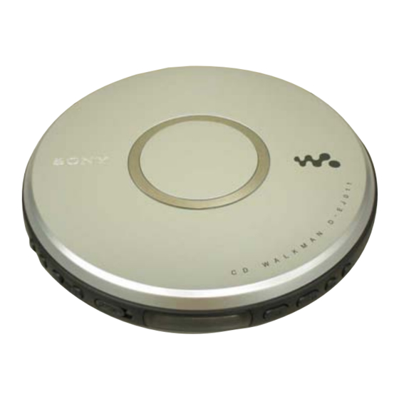
Sony D-EJ011 Service Manual
Portable cd player
Hide thumbs
Also See for D-EJ011:
- Operating instructions (2 pages) ,
- Specification sheet (2 pages) ,
- Operating instructions (1 page)
Table of Contents
Advertisement
SERVICE MANUAL
Ver. 1.0 2006.12
System: Compact disc digital audio system
Laser diode properties
Emission duration: Continuous
Laser output: Less than 44.6 µW (This output is the
value measured at a distance of 200 mm from the
objective lens surface on the optical pick-up block
with 7 mm aperture.)
Power requirements
• Two LR6 (size AA) batteries: 1.5 V DC × 2
Dimensions (w/h/d) (without projecting parts and controls)
Approx. 139.8 × 27.9 × 139.8 mm
Mass (excluding accessories)
Approx.188 g
Operating temperature 5°C - 35°C (41°F - 95°F)
Sony Corporation
9-887-511-01
Personal Audio Division
2006L02-1
Published by Sony Techno Create Corporation
© 2006.12
D-EJ011
Model Name Using Similar Mechanism
CD Mechanism Type
Optical Pick-up Name
SPECIFICATIONS
Battery life* (approx. hours)
(When the CD player is used on a flat and stable
place.)
Playing time varies depending on how the CD player
is used.
G-PROTECTION
Two Sony alkaline batteries LR6 (SG)
(produced in Japan)
* Measured value by the standard of JEITA (Japan
Electronics and Information Technology Industries
Association).
• The indicator sections of
remaining battery power. One section does not
always indicate one-fourth of the battery power.
Design and specifications are subject to change
without notice.
Supplied accessories
Headphones (1)
E Model
D-EJ010
CDM-3525A
DAX-25E
G-on
G-off
16
11
roughly show the
PORTABLE CD PLAYER
Advertisement
Table of Contents

Related Manuals for Sony D-EJ011


Summary of Contents for Sony D-EJ011
- Page 1 G-PROTECTION G-on G-off with 7 mm aperture.) Two Sony alkaline batteries LR6 (SG) Power requirements (produced in Japan) • Two LR6 (size AA) batteries: 1.5 V DC × 2 * Measured value by the standard of JEITA (Japan...
-
Page 2: Table Of Contents
COMPONENTS IDENTIFIED BY MARK 0 OR DOTTED LINE WITH MARK 0 ON THE SCHEMATIC DIAGRAMS AND IN THE PARTS LIST ARE CRITICAL TO SAFE OPERATION. REPLACE THESE COMPONENTS WITH SONY PARTS WHOSE PART NUMBERS APPEAR AS SHOWN IN THIS MANUAL OR IN SUPPLEMENTS PUBLISHED BY SONY. -
Page 3: Servicing Notes
D-EJ011 SECTION 1 SERVICING NOTES • Method: NOTES ON HANDLING THE OPTICAL PICK-UP Emission of the laser diode is visually checked. BLOCK OR BASE UNIT 1. Open the upper lid. The laser diode in the optical pick-up block may suffer electrostatic 2. -
Page 4: Disassembly
D-EJ011 SECTION 3 DISASSEMBLY • This set can be disassembled in the order shown below. 3-1. DISASSEMBLY FLOW 3-2. CABINET (INNER) ASSY, CABINET (LOWER) ASSY (Page 4) 3-3. OPTICAL PICK-UP (CDM-3525A), MAIN BOARD (Page 5) Note: Follow the disassembly procedure in the numerical order given. -
Page 5: Optical Pick-Up (Cdm-3525A), Main Board
D-EJ011 3-3. OPTICAL PICK-UP (CDM-3525A), MAIN BOARD 3 optical pick-up CDM-3525A 1 CN501 2 Unsolder four lead wires 4 MAIN board To/From Optical device CDM-3525A MAIN Board (side A) cabinet (lower) assy... -
Page 6: Electrical Adjustment
D-EJ011 SECTION 4 ELECTRICAL ADJUSTMENTS The CD section adjustments are done automatically in this set. Procedure: 1. Make a solder bridge to short SL801 (OPEN) on the MAIN Adjusting Procedure: board side B. 1. Perform check in the order given. - Page 7 D-EJ011 SECTION 5 DIAGRAMS • Note for Printed Wiring Boards and Schematic Diagrams Note on Printed Wiring Boards. Note on Schematic Diagrams. • All capacitors are in µF unless otherwise noted. (p: pF) • X : parts extracted from the component side.
-
Page 8: Diagrams 5-1. Block Diagram
D-EJ011 5-1. BLOCK DIAGRAM IC602 SDRAM(16M) DQ0-15 A0-11 2,3,5,6,8,9,11,12,39, 19-24,27-32 17 16 15 14 36 35 34 40,42,43,45,46,48,49 IC301 Q602 HEADPHONE AMP OPTICAL DEVICE 43-32 80 79 47-62 44 45 46 28 29 (CDM-3525A) LDACO OUT1 MEMORY CONTROLLER OP IC... -
Page 9: Main Board (Side A)
D-EJ011 :Uses unleaded solder. 5-2. PRINTED WIRING BOARD – MAIN BOARD (SIDE A) – MAIN BOARD (SIDE A) • Semiconductor R205 Location R206 R106 C208 Ref. No. Location C306 D401 R201 D403 C303 D803 C630 IC301 R616 IC601 R104 R103... -
Page 10: Printed Wiring Board - Main Board (Side B), Jack Board
D-EJ011 :Uses unleaded solder. 5-3. PRINTED WIRING BOARD – MAIN BOARD (SIDE B) – MAIN BOARD (SIDE B) • Semiconductor Location C110 SL801 S811 Ref. No. Location C627 (OPEN) (OPEN) D404 X601 IC401 L301 IC602 IC602 R626 IC801 R625 R107... -
Page 11: Schematic Diagram - Main Board (1/2)
D-EJ011 5-4. SCHEMATIC DIAGRAM – MAIN BOARD (1/2) – • See page 7 for Waveforms. • See page 13, 14 for IC Block Diagrams. IC B/D IC B/D M121616A-7T(J) IC B/D D-EJ011... - Page 12 D-EJ011 5-5. SCHEMATIC DIAGRAM – MAIN BOARD (2/2) – • See page 7 for Waveforms. • See page 15 for IC Pin Function Description. D-EJ011...
-
Page 13: Ic Block Diagrams
D-EJ011 • IC Block Diagrams IC301 BH3544F-FE2 BIAS MUTE IC401 BH6575FV-E2 VSYS – CONV VSYS PRE-DR PRE-DR DETECT – DC/DC – CONVERTER MUTE1 SYSTEM PRE-DR PRE-DR MUTE34 RESET SYSTEM... - Page 14 D-EJ011 IC601 BU9352KV 60 DQ10 AVDD1 59 DQ11 1 BIT DAC 58 DQ12 VBIAS 57 DQ13 AC_GAIN 56 DQ14 BD_GAIN 16K SRAM 55 DQ15 x8 OVER SAMPLING 54 DQ00 DIGITAL FILTER 53 DQ01 52 DQ02 DIGITAL DIGITAL 51 DQ03 SIGNAL...
-
Page 15: Ic Pin Function Description
D-EJ011 5-6. IC PIN FUNCTION DESCRIPTION • IC801 BU1377KS2 (SYSTEM CONTROLLER) Pin No. Pin name Description 1 to 18 SEG0 to SEG17 LCD segment output SEL_CHG Not used (fixed at “L”) SEL_CEX Destination select (fixed at “L”) CHARGE_CTL Not used (OPEN) - Page 16 D-EJ011 Pin No. Pin name Description – Power supply for CPU and I/O DC_IN DC IN voltage monitoring input BATT+ Batt+ terminal voltage monitoring input BATT– Connect to GND KEY1 Connect to GND TEST MODE Test mode terminal WREM Wired remotecontroler key detection input. Not used (fixed at “H”)
-
Page 17: Exploded Views
D-EJ011 SECTION 6 EXPLODED VIEWS NOTE: The components identified by mark 0 or • -XX and -X mean standardized parts, so they • Color Indication of Appearance Parts dotted line with mark 0 are critical for safety. may have some difference from the original Example: one. -
Page 18: Electrical Parts List
D-EJ011 SECTION 7 MAIN ELECTRICAL PARTS LIST NOTE: The components identified by mark • Items marked “*” are not stocked since they • Due to standardization, replacements in the 0 or dotted line with mark 0 are parts list may be different from the parts are seldom required for routine service. - Page 19 D-EJ011 MAIN Ref. No. Part No. Description Remark Ref. No. Part No. Description Remark < IC > R403 1-216-821-11 METAL CHIP 1/10W R404 1-216-809-11 METAL CHIP 1/10W IC301 8-759-588-61 IC BH3544F-FE2 IC401 6-704-047-01 IC BH6575FV-E2 R405 1-218-873-11 METAL CHIP 0.5%...
- Page 20 D-EJ011 MAIN Ref. No. Part No. Description Remark Ref. No. Part No. Description Remark < SWITCH > S801 1-786-865-11 SWITCH, KEYBOARD (u) S802 1-786-865-11 SWITCH, KEYBOARD (>) S803 1-786-865-11 SWITCH, KEYBOARD (.) S804 1-786-865-11 SWITCH, KEYBOARD (VOL –) S805 1-786-865-11 SWITCH, KEYBOARD (VOL +)
- Page 21 D-EJ011 MEMO...
-
Page 22: Revision History
D-EJ011 REVISION HISTORY Clicking the version allows you to jump to the revised page. Also, clicking the version at the upper right on the revised page allows you to jump to the next revised page. Ver. Date Description of Revision...