Table of Contents
Advertisement
Quick Links
This service manual provides a variety of service
information.
It contains the mechanical structure of the CD-
R/RW Drive and the electronic circuits in
schematic form. This CD-R/RW Drive was
manufactured and assembled under our strict
quality control standards and meets or exceeds
industry specifications and standards.
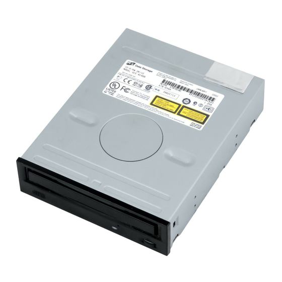
This CD-R/RW drive is an internal drive unit
designed for use with IBM PC, HP Vectra, or
1. General
1) Enhanced IDE interface.
2) Internal 5.25 inch, halfheight CD-R/RW Drive.
3) 8 Mbytes buffer memory.
4) Audio CD like tray loading of a disc without using a caddy.
5) Power loading and power ejecting of a disc. The disc can also be ejected manually.
6) Supports Power saving mode and Sleep mode.
7) Vertical and Horizontal operation.
8) ExacLink Function.
2. Supported disc formats
1) Reads and writes data in each CD-ROM, CD-ROMXA, CD-I FMV, Video CD, and CD-EXTRA
2) Reads data in Photo CD (Single and Multi session).
3) Reads and writes standard CD-DA.
4) Reads and writes CD-R discs conforming to "Orange Book Part 2".
5) Reads and writes CD-RW discs conforming to "Orange Book Parts 3".
3. Supported write method
1) Disc at once (DAO), Session at once (SAO), Track at once (TAO), Variable packet, Fixed packet, and
Multi-session.
4. Performance
1) Random 110 ms average access time.
2) CD-R Record speed : 8X, 12X, 16X, 16-24X Z CLV.
3) CD-RW Record speed : 2X, 4X, 10X.
4) CD-ROM : Max 6,000 KB/s(Max 40x) Sustained Transfer rate.
5) Supports real time error correction and real time layered error correction at each speed.
6) PIO Mode 4, Multi DMA Mode 2 .
7) Multimedia MPC-3 Spec compliant.
8) Support CD-TEXT read/write.
5. Audio
1) Output 16 bit digital data over ATA interface.
2) 8 Times Digital Filter for CD Audio
3) Software Volume Control
4) Equipped with audio line output and headphone jack for audio CD playback.
5) Front panel Volume Control for Headphone Output.
INTRODUCTION
compatible computer. It can write as much as 700
Mbytes of digital data into CD-R/RW disc, and can
read as much as 650 Mbytes of digital data stored
in a CD-ROM, CD-R and CD-RW disc.
This CD-R/RW Drive can easily meet the
upcoming MPC level 3 specification, and its
Enhanced Intelligent Device Electronics (E-IDE)
and ATAPI interface allows Plug and play
integration in the majority of today's PCs without
the need of an additional interface card.
FEATURES
3
Advertisement
Table of Contents

Related Manuals for LG GCE-8240B


Summary of Contents for LG GCE-8240B
- Page 1 INTRODUCTION compatible computer. It can write as much as 700 This service manual provides a variety of service Mbytes of digital data into CD-R/RW disc, and can information. read as much as 650 Mbytes of digital data stored It contains the mechanical structure of the CD- in a CD-ROM, CD-R and CD-RW disc.
-
Page 2: System Requirements
SPECIFICATIONS 1. SYSTEM REQUIREMENTS -CPU: IBM Compatible Pentium 350MHZ (or faster) (For 24X Write speed, 500MHz or faster recommended.) -64MB Memory or greater 2. SUPPORTING OPERATING SYSTEM • DOS 3.1 or Higher • Solaris Ver 2.4 or higher • Windows 95/98/2000/ME/XP •... -
Page 3: Drive Performance
Separation Frequency + 2dB + 3 dB 20Hz~20KHz 0 dB No Filter at 47 kΩ Response * GCE-8240B FUNCTION TABLE MODEL Funtion GCE-8240B • CD-R Writing speed 8x/12x/16x/16x-24x ZCLV Data writing • CD-RW Writing speed 2x/4x/10x Data writing • CD-ROM Reading speed... -
Page 4: Location Of Customer Controls
LOCATION OF CUSTOMER CONTROLS Front Panel Emergency Eject Hole Disc Tray Stop/Eject Button Volume Control Drive Activity Indicators Headphone Jack 1. Disc tray 5. Headphone jack This is the tray for the disc. Place the disc on the This jack is for connecting headphones or mini- ejected disc tray, then lightly push the tray (or speakers. -
Page 5: Rear Panel
Rear Panel IDE Interface Connector Analog Audio Output Connector Jumper Connector Power Connector Digital Audio Output Connector 1. Power Connector 3. Jumper Connector Connects to the power supply (5-and 12-V DC) of This jumper determines whether the drive is the host computer. configured as a master or slave. -
Page 6: Cabinet And Circuit Board Disassembly
DISASSEMBLY 1. CABINET and CIRCUIT BOARD 1-3. Cabinet and Main Circuit Board A. Remove the Cabinet in the direction of arrow (4). DISASSEMBLY (See Fig. 1-3) 1-1. Bottom Chassis B. Release 2 hooks (a) and remove the CD Tray A. Release 4 screws (A) and remove the Bottom Chassis drawing forward. - Page 7 2-2. Pick-up A. Release 2 screws (C) and remove the Pick-up. Pick-up Unit Pick-up Fig. 2-2...
- Page 8 GLOSSARY ATIP Absolute Time in Pre-groove. With an additional modulation of the “Wobble”, the “Groove” contains a time code information. Wobble The pre-groove in the Disc is not a perfect spiral but is wobbled. With : – A typical amplitude of 30 nm –...
-
Page 9: The Differences Of Cd-R/Cd-Rw Discs And General Cd-Rom
The differences of CD-R/CD-RW discs and General CD-ROM 1. Recording Layer Recordable CD has a wobbled pre-groove on the surface of disc for laser beam to follow track. Track pitch(p) a=30nm Read-only Disc CD-ROM (READ-ONLY DISC) Radial Direction Radial Error Signal 0.4~0.5 um Groove Land... -
Page 10: Disc Materials
3. Disc Materials 1) CD-ROM disc • It is composed of Silver _ colored aluminum plate and Reflective layer. • Groove (Pit) of aluminum plate make a track. • Laser wavelength : 780 nm, Laser Power (Read): 0.5mW • Signal is detected by the difference of reflective beam intensity between “pit”... -
Page 11: Reading Process Of Optical Disc
3) CD-RW Disc Label Printing Protective Layer Dielectric Layer(TL) Reflective Layer Dielectric Layer(UL) Substrate (Polycarbonate) Groove Laser Beam • It is composed of polycarbonate layer, alloy(silver, arsenic) layer, aluminum reflectivity layer, protective layer. • An crystalized alloy layer is transformed into noncrystalized by the laser heat. Therefore, writing and reading is enabled by the difference of reflectivity. -
Page 12: Writing Process Of Cd-R Disc
5. Writing Process of CD-R Disc Incident (Write) Laser Power (Read) (Read) Laser Spot a b c d e f Position (Time) Laser Below "ORP"– Mark Too Short Spot Reflected At Optimum Record Power ("ORP") Light Signal Above "ORP" – Mark Too Long Recorded Mark Time... - Page 13 7. Organization of the PCA, PMA and Lead-in Area 1) Layout of CD-ROM disc Disc Center Diameter 120 mm Diameter 46 mm Diameter 15 mm Center hole Clamping and Label Area Information Area Read Only Disc Lead-in Area Program Area Lead-out Area 2) Layout of CD-R/RW disc Disc Center...
-
Page 14: Function Of Pca And Pma Area
8. Function of PCA and PMA area 1) PCA (Power Calibration Area) • PCA area is used to determine the correct Laser Power for a disc. – Method 1 : PCA area is divided by a track. – Method 2 : The previous Calibration value is referred. –... -
Page 15: Writing Process Of Disc
2) ROPC (Running Optimum Power Control) • Variable primary factor of Optimum Power – Change of Power sensitivity on the Disc. (limited to 0.05 *Po) – Wavelength shift of the laser diode due to the operating temperature change. – Change of the Spot aberration due to the Disc skew, Substrate thickness, Defocus. -
Page 16: Internal Structure Of The Pick-Up
INTERNAL STRUCTURE OF THE PICK-UP 1. KRS-310B Circuit Diagram 2 Axis Actuator FCS + FCS - TRK + TRK - PDIC RF SUM PDGND PDVC PDVCC FPDO IC2 FPDIC FPDVCC FPDGND FPDVC LDVCC LDVCC VRDC VWDC1 VWDC2 LDGND LDGND VOUT PDIN VREF OSCEN... -
Page 17: Signal Detection Of The P/U
2. Signal detection of the P/U Infrared Iaser Pick-Up module Focusing Tracking Photo Diode 1) Focus Error Signal ==> (A+C)-(B+D) This signal is generated in RF IC (IC401 : CXA2638R) and controls the pick-up’s up and down to focus on Disc. -
Page 18: Alpc (Automatic Laser Power Control) Circuit
DESCRIPTION OF CIRCUIT 1. ALPC (Automatic Laser Power Control) Circuit 1-1. ALPC Loop Circuit 3.3V R422 FPDVC C456 R423 IC403 C455 PN401 FPDO IC401 CXA2638R MPXOUT (Read) (testmode) RFPDG VRDCN 20dB/26dB FPDO R410 VRDC VRDC A:OFF C433 B:ON RREFSE R247 H:RREF RFPDSH L:OPEN... - Page 19 1-2. ALPC(Automatic Laser Power Control) Circuit Operation This circuit consists of Feedback Loop to maintain light output of the Laser Diode(FPDO). Feedback signal, output voltage from PD(Photo Detector) of P/U, is used monitor the light power of Laser Diode. 1) Read Loop RREF(Read Reference Voltage) of IC401(CXA2638R) Pin 96, which is from DAC(IC403) Pin 18, is the reference level of the Read Loop part of this ALPC Circuit.
- Page 20 2. RF Amplifier Circuit Block Diagram...
-
Page 21: Focus/Tracking/Sled Servo Circuit
3. Focus/Tracking/Sled Servo Circuit 3-1. Focus, Tracking & Sled Servo Process Focus, Tracking Servo IC401 CXA2638R Pick- up Focus Error Detector A,B,C,D A,B,C,D,E,F,G,H Track Error Detector A,B,C,D E,F,G,H Tracking Focusing Actuator IC201 Servo Control OTI9797 LEVEL SHIFT LEVEL SHIFT Low freq Gain Filter Ditital EQ IC501 BD7902C... -
Page 22: Focus Servo
3-2. Focus Servo The aim of Focus Servo is to maintain the distance between object lens of P/U and disc surface, so that the detected RF signals (A, B, C, D) can be maximized. Focus Servo is based on focus error (FE) signal which is generated from focus error detection block in CXA2638R(IC401) using Astigmatism Method. -
Page 23: Spindle Servo Circuit
4. Spindle Servo Circuit 4-1. Spindle Servo Process IC401 CXA2638R Pick- up ATFG Wobble Signal Generator EQRFP Spindle Motor IC201 OTI9797 IC501 BD7902C Hall Sensor CD-DSP/SERV O CD EFM CLV Decode PLL CAV x32 Frequency Controller LOCK FILTER DEFS MOTOR SPEED ATIP CLV, FG CONTROLLER IC 301... -
Page 24: Major Ic Internal Block Diagram And Pin Description
MAJOR IC INTERNAL BLOCK DIAGRAM AND PIN DESCRIPTION IC401 (CXA2638R) : CD-R/RW Analog Signal Processor Block Diagram 74 73 72 71 70 69 68 67 66 65 64 63 62 61 60 59 58 57 56 55 54 53 52 51 PHC1 50 XTAND BHC1... -
Page 25: Pin Assignment
• Pin Assignment Pin no Symbol Description FVREF Reference voltage of APC input signal Input of Main beam signal(A) Input of Main beam signal(B) Input of Main beam signal(C) Input of Main beam signal(D) HAVC Reference Voltage of Main and Side beams Input of Side beam signal (E) Input of Side beam signal (F) Input of Side beam signal (G) - Page 26 Pin no Symbol Description XTOK Output of Out-of -Track Amplitude Detection signal DVCC Digital power Chip power save control (H: power ON, L: Power OFF) RFCTC2 External Capacitor connection of Peak Hold Time Constant for RFRP signal RFCTC1 External Capacitor connection of Bottom Hold Time Constant for RFRP signal TOK2C External Capacitor connection for Retriggerable mono multi Time Constant TOK1C...
- Page 27 IC201(OTI-9797) : CD-R/RW Encoder/Decoder/Write Strategy Chip Block Diagram...
- Page 28 CLOCK Pin Name Pin # Type Description Crystal In: System clock XOUT Crystal Out: System Clock ATIPCK / ATIP Clock Out WBLCLK ENCLK Encoder Clock Input CLKOUT / General Purpose Clock Output ARST# CD-ENCODER INTERFACE 2.4.2 CD-ENCODER INTERFACE Pin Name Pin # Type Description...
- Page 29 Pin Name Pin # Type Description EFMNT2 / EFMNT2: EFM pit pattern length indicator / EFMNT2’ / EFMN : Non-Delayed EFM Pit Pattern Length Indicator / ELPBS2 ELPBS2: External Low Pass Filter Band Switch EFMNT3 / EFMNT3: EFM pit pattern length indicator / EFMNT3’...
- Page 30 WOBBLE MOTOR INTERFACE Pin Name Pin # Type Description Reverse Detect Motor Drive: Indicates spindle motor is rotating in reverse REVDET direction FG IN: HG (tachometer) pulse input Motor Drive On: Enables spindle motor drive Short Brake: Stops spindle motor by applying a short pulse to the motor SBRK winding A T IPCK /...
- Page 31 Pin Name Pin # T ype Description RP Zero Crossing: Used for fine search. TE Zero Crossing: Track crossing signal input used in conjunction with RX to perform fine searches. Center Position Error LDON / Laser Diode On / CAV Write N Divider: MUXing of this pin is controlled by bit NDIVOUT ATIPN (18Fh.7).
- Page 32 AUDIO INTERFACES Pin Name Pin # Type Description Multiple I/O 0: MIO0 is used to output several internal test signals. DEFAULT Serial Data: This signal is for 16-bit PCM serial audio data. MIO0 / It can be used to send audio data to an external or internal OTI-9797 DAC. L–...
- Page 33 ATAPI/SCSI PASS-THROUGH HOST INTERFECE Pin Name Pin # Type Description HD15 HD14 HD13 HD12 HD11 HD10 Host Data Bus (ATAPI & SCSI DMA Modes) HD7=I/O ATA Write Strobe (ATAPI Mode): During PIO and DMA transfers, the host uses this signal to write data to the device. ATA Stop Ultra DMA Burst (ATAPI Mode): During Ultra DMA transfers, HWR#/ the host uses this signal to halt a burst transfer.
- Page 34 Pin Name Pin # Type Description HA2 / ATA Address (ATAPI Mode): The host uses the 3-bit ATA address to select an ATAPI control command block register or data port. ATA Address 0 (ATAPI Mode): The host uses the 3-bit ATA address to select an ATAPI control command block register or data port.
- Page 35 Pin Name Pin # Type Descrip tion ATA Interrupt Request (ATAPI Mode): This signal is used to interrupt the host system. HIRQ is controlled by bit HINTRQ (02Eh.3). HIRQ / SIRQ# SCSI Interrupt (SCSI DMA Mode): This signal is asserted by the SCSI Protocol Controller to interrupt the system controller.
- Page 36 SYSTEM CONTROLLER INTERFACE Pin Name Pin # Type Description UA15 UA14 UA13 System Controller Address 15 8 Bus: This bus is the upper 8-bits of the 16- UA12 bit system controller address. In register access mode (UCS0# asserted), UA11 UA15 are not decoded.
- Page 37 Pin Name Pin # Typ e Description System Controller-RAM Transfer Ready: This signal is asserted low to extend a system controller-RAM access until the RAM data is ready to be read or written. If direct-RAM access is used (UCS1# asserted), a system controller with a wait-state insertion input must be used.
- Page 38 BUFFER MEMORY INTERFACE Pin Name Pin # Type Description SDRAM System Clock: RCLK clocks data and commands to/from the RCLK SDRAM. RCLKE SDRAM Clock Enable: RCLKE is asserted high to enable the SDRAM clock. RCS# SDRAM Chip Select: RCS# is asserted low to select the SDRAM. DRAM Row Address 13: Row address 13 in EDO DRAM Mode RAD13 / SDRAM Bank Address 2: When RRCF (0CCh...
- Page 39 Pin Name Pin # Typ e Description RD15 / RAM Data 15 / Drive Jumper: RD15 is bit 15 of the RAM data bus. It is also used as the DJ for the host interface. RD14 RAM Data 14: RD14 is bit 14 of the RAM data bus. RAM Data Bus 13/CPU Type: RD13 is bit 13 of the RAM Data Bus.
- Page 40 Pin Name Pin # Typ e Description DRAM Column Address Strobe High: For dual-CAS# DRAM Mode, RCASH# is the column address strobe for the upper data byte (R RCASH# / DRAM Write Enable High: For dual-WE# DRAM mode, RWEH# enables RWEH# / writing of the upper data byte (RD UDQM...
- Page 41 IC301 (MB90F482) : Micom Block Diagram Clock control X0, X1, RST, circuit X0A, X1A FMC16X series MD2, 1, 0 Interrupt controller PPG0, 1 PPG2, 3 8-/16-bit PPG PPG4, 5 AIN0, 1 BIN0, 1 8-/16-bits U/D counter Prescaler ZIN0, 1 SIN0 UART SOT0 Chip selects...
-
Page 42: Pin Description
•Pin Description Circuit Type LQFP Pin Name Function Oscillator pin Oscillator pin 32 kHz Oscillator pin 32 kHz Oscillator pin RSTX Reset input pin General-purpose I/O ports P00 to P07 A pull-up resistor can be attached using the pull-up resistor setting register (RDR0) (RD07 to RD00 = 1). - Page 43 LQFP Pin Name Circuit Type Function General-purpose I/O ports In the external bus mode, the pin functions as an external address pin. (CMOS/H) AIN0 The pin is an 8-/16-bit up-and-down timer input pin (ch0). General-purpose I/O port In the non-multiplex bus mode, the pin functions as an external address (CMOS/H) pin.
- Page 44 LQFP Pin Name Circuit Type Function General-purpose I/O port In the external bus mode, the pin functions as ALE pin. (CMOS) In the external bus mode, the pin functions as an address capture enable signal (ALE) pin. General-purpose I/O port In the external bus mode, the pin functions as the RDX pin.
- Page 45 LQFP Pin Name Circuit Type Function General-purpose I/O port SOT0 (CMOS) The pin functions as an UART data output pin. General-purpose I/O port SCK0 (CMOS/H) The pin functions as an UART clock I/O pin. General-purpose I/O port (CMOS/H) TIN0 The pin functions as the event input pin of the 16-bit reload timer. General-purpose I/O port TOT0 (CMOS/H)
- Page 46 IC501 (BD7902C): Spindle Motor and 5ch Actuator Driver Block Diagram DVCC FCIN TKIN LDO+ LDO- TKO+ PGND1 TKO- FCO+ SPVM1 FCO- PGND2 AGND SLO1+ SPVM2 SLO1- SPRNF SLO2+ SLO2- CTL1 SLGND CTL2 SLRNF2 SPIN SLRNF1 DGND SLVDD LDIN SLIN2 SLIN1...
- Page 47 • Pin Description Terminal Symbol Terminal function Terminal Symbol Terminal function Hall amp.U positive input DVCC PWM block control power supply Hall amp.U negative input FCIN Focus driver input Hall amp.V positive input TKIN Tracking driver input Hall amp.V negative input BTL pre and Loading power supply Hall amp.W positive input LDO+...
- Page 48 IC402(BU2500FV) 1) The BU2500FV is an integrated circuit semiconductor of CMOS structure with 12 channels of built-in D-A converters with output buffer operational amplifiers. 2) Outputs of 12 channels are used for adjustment/control of servo circuits and references. Block Diagram Ao12 Ao11 12-BIT SHIFT REGISTER...
-
Page 49: Troubleshooting Guide
TROUBLESHOOTING GUIDE Reset or Power Check. Check it after connecting the power cable only on interface cable for NO Reset or Power ON. Are the pin 41 • Check the power(12V, 5V) short. and 44 of PN201 +12V and +5V •... - Page 50 System Check. Load tray without inserting disc. Does Tray operate normally? Go to “Tray operating is abnormal” Go to “Sled operating is abnormal” Does Pick-up move to inside? Does Spindle Motor Go to “Spindle operating is rotate in a moment? abnormal”...
- Page 51 Tray operating is abnormal. Tray open/close doesn’t work. Is the input voltage • Check the connection of IC301 pin 20. 0V at IC301 pin 20 when push the • Replace the SW802(Eject s/w) SW802? • Check the connection of IC402 pin 7. •...
- Page 52 Sled operating is abnormal. • Is there Sled Check the control signal output? Replace the IC301(MICOM). communication line between IC402 (IC402 pin 8, 9) and IC301(MICOM). Replace the IC402(BU2500FV). Aren’t Is there MUTE1 signla “H” Check the connection of IC301 Sled drive voltage output? and MUTE2 signal “H”? (IC501 pin 34, 35, 36, 37)
- Page 53 Spindle operating is abnormal Is there Is there • Check the connection of IC201 pin 2. Spindle control signal input? DMO signal input ? • Replace the IC201(OTI-9797). (IC501 pin 24) (IC503 pin 5) Is there • Check the IC503. Spindle control signal output? •...
- Page 54 Focus Actuator operating is abnormal • Is there Focus Check the connection of IC201 pin 207. • Search control signal input? Check the communication line between (IC501 pin 53) IC201 and IC301. • Replace the IC201 (OTI-9797). Aren’t • Check the connection of IC201 pin Is there Focus MUTE1 signal “H”...
- Page 55 Spindle control is abnormal 2 (CD-ROM Disc) Is there RRF signal output? Go to “RF output is abnormal” (IC401 pin 85) Does Tracking Servo Go to “Track Servo is unstable” operate normally? Is there RECD, signal output normally? Go to “RF output is abnormal” (IC401 pin 37) Replace the IC301(MICOM).
- Page 56 RF output is abnormal Is there PICK UP (A, B, C, D) • Check the PICK UP FFC. output normally? Go to “Laser is abnormal” • Replace the PICK UP. (PN401 pin 7, 8, 15, 16) Is RRF signal output normal? •...
- Page 57 Track Servo is unstable Is TE signal Is PICK UP • Check the PICK UP FFC. output normal in Focusing (E, F, G, H) output normal? • Replace the PICK UP. ON and Tracking OFF? (PN401 pin 6, 9, 14, 17) (IC401 pin 58) Check the IC401(CXA2638R).
- Page 58 Laser is abnormal Execute ‘B.Check ALPC Parameters’ of ‘How to use Test Tool (Dragon)’ Is EEPROM Data valid? Execute ‘D.Laser Inspection’ of Execute ‘C.Laser Power Setup’ of ‘How to use Test Tool(Dragon)’ ‘How to use Test Tool(Dragon)’ OFF LEVEL NG? Normal VRDC NG? VWDC1 NG?
- Page 59 LD CHECK (Not Read) Execute ‘E. ALPC Test for AS’ of ‘How to use Test Tool(Dragon) : ‘VRDC Loop [Read Mode]’ • Check the connection of IC301 pin 12. PN401 Pin 33(ENBL)=H? • Check and replace the IC301(MB90F482). • Check the connection of IC402 Pin 18 •...
- Page 60 LD CHECK (Not Recorded) Execute ‘E.ALPC Test For As’ of ‘How to use Test Tool(Dragon)’: ‘CW Power Test’ • Check the connection of IC301 pin 12. PN401 Pin 32(ENBL) = ‘H’? • Check and replace the IC301(MB90F482). • PN401 Pin 30 Check the connection of IC201 pin 183, 184.
- Page 61 Does the disc if the disc has long width have any Dust, Scratch, Scratch, change it. Fingerprint...? Use LG bundle Software (Write Tool & Version) Is the write Tool(version) - Roxio ECDC 5.1(61), supported by LG CD-RW Direct CD 5.10 (116) Drive? Check disc information on Writng Tool.
- Page 62 Writing Part Check. Refer “Laser is abnormal”. Load tray with CD-R/RW Disc. Run the Writing Tool (Easy CD Creator). Run the Writing with Tool (Easy CD Creator). Do the IC301(MICOM) pin 22 and pin 23 output toggle The blink LED1 when writing started? signals during Writing?
- Page 63 ALPC Logic Circuit Check. Execute ‘E.ALPC Test For AS’ of ‘How to use Test Tool(Dragon)’ : ‘CD-R Rec Mode’ • Check the connection of IC301 pin 5. IC301 Pin 7 (WR/RE) = ‘H’? • Check and replace the IC301. • Check the connection of IC201 pin 166.
- Page 64 Execute ‘E.ALPC Test For AS’ of ‘How to use Test Tool(Dragon)’ : ‘CD-RW Rec Mode’ • Check the connection of IC301 pin 5. IC301 Pin 7 (WR/RE) = ‘H’? • Check and replace the IC301. • Check the connection of IC201 pin 166. IC205 Pin5 (WGATE) = ‘H’? •...
- Page 65 No audio output Insert the audio Disc. AUD_MUTE : ‘L’? (IC301 Pin 73) Do LOUT, ROUT signals output? • Check and replace the IC201. (IC201 Pin 151, 154) Do audio Line signals output? • Check the connection of L/R OUT. (PN201 Pin 51, 54) Adjust H/P volume max.
- Page 66 Confirm the Beta measurement circuit. Insert Test Disk (TCD-T84) and play 1x. • Check the connection of IC401 pin 85. IC401 pin 85(RRF)? • Check and replace IC401 (CXA2638R). • Check the connection of IC401 pin 84. IC401 pin 84(RRFIN)? •...
- Page 67 1. Install GCE-8240B –> PC Power ON –> Execute Windows. 2. Execute Dragon for JE2.exe on Windows (Dragon for JE2.exe & Dragon.cfg should be on same Directory). 3. If you use GCE-8240B, “Dragon(Ver x.xx)” will be displayed on the Window Frame. 4. Select I/F Setup on the menu bar.
- Page 68 C. Laser Power Setup (VWDC1 / VWDC2 re-setup) 1. Remove disc on the tray. 2. Select ALPC/OPC on the menu bar, and then select Laser Power Setup menu. 3. Setup LD Power meter (Frequency : 780nm, Measure Range : 0.01mW unit). 4.
- Page 69 D. Laser Inspection (VRDC/VWDC/FPD Level Check) 1. Remove disc on the Tray. 2. Select ALPC/OPC on the menu bar and select Laser Inspection menu, then Laser Power Test window will appear. 3. Click Trigger button, then the result will displayed with OK or NG separately. 4.
- Page 70 E. ALPC Test for AS 1. Remove disc on the Tray. 2. Select ALPC/OPC on the menu bar and select ALPC Test for AS menu, then window will appear. 3. Select Specific mode of ALPC Test mode and click Trigger button, then LD will be on. 4.
-
Page 71: Functional Block Diagram
BLOCK DIAGRAM FUNCTIONAL BLOCK DIAGRAM X201 33.8688MHz IC201 Cable IC401 OTI-9797 Optical CXA2638R Pick-up RF Amp. DECODER KRS-310B ENCODER Wobble ATIP Demodulator ALPC IC202 Wirte Strategy Data SDRAM Spindle Motor 8M Byte MSDH-R001A/ SLED Motor SSC35A/C-SP IC203 IC301 EEPROM 32 Kbit MB90F482 SERVO/DSP FOCUS... - Page 72 EXPLODED VIEW PBM00 (MAIN C.B.A)