Table of Contents
Advertisement
SERVICE MANUAL
Ver 1.1 2001. 12
• HCD-DX50/RG80 are the tuner,
deck, CD and amplifier section in
MHC-DX50/RG80.
Sony Corporation
9-929-589-12
2001L1600-1
Home Audio Company
© 2001.12
Published by Sony Engineering Corporation
HCD-DX50/RG80
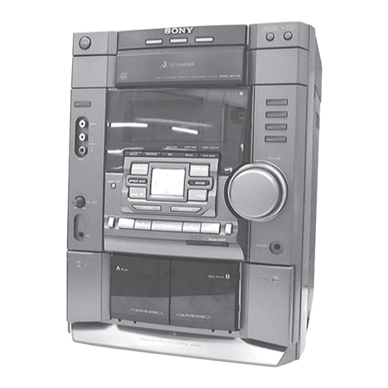
Photo : HCD-DX50
SPECIFICATIONS
Model Name Using Similar Mechanism
CD
CD Mechanism Type
Section
Base Unit Name
Optical Pick-up Name
Tape deck
Model Name Using Similar Mechanism
Section
Tape Transport Mechanism Type
MINI HI-FI COMPONENT SYSTEM
Canadian Model
HCD-RG80
Australian Model
E Model
HCD-DX50
NEW
CDM58E-30BD60
BU-30BD60
A-MAX.3
NEW
TCM-230PWR41C
— Continued on next page —
Advertisement
Table of Contents

Related Manuals for Sony HCD-DX50


Summary of Contents for Sony HCD-DX50
- Page 1 HCD-DX50/RG80 SERVICE MANUAL Canadian Model HCD-RG80 Ver 1.1 2001. 12 Australian Model E Model HCD-DX50 • HCD-DX50/RG80 are the tuner, Photo : HCD-DX50 deck, CD and amplifier section in MHC-DX50/RG80. Model Name Using Similar Mechanism CD Mechanism Type CDM58E-30BD60 Section...
- Page 2 CRITIQUES POUR LA SÉCURITÉ DE FONCTIONNEMENT. NE COMPONENTS WITH SONY PARTS WHOSE PART NUMBERS REMPLACER CES COMPOSANTS QUE PAR DES PIÈSES SONY APPEAR AS SHOWN IN THIS MANUAL OR IN SUPPLEMENTS DONT LES NUMÉROS SONT DONNÉS DANS CE MANUEL OU PUBLISHED BY SONY.
-
Page 3: Table Of Contents
HCD-DX50/RG80 TABLE OF CONTENTS 1. GENERAL ·········································································· 4 SAFETY CHECK-OUT After correcting the original service problem, perform the 2. DISASSEMBLY ······························································· 7 following safety checks before releasing the set to the customer: 3. TEST MODE ···································································· 12 Check the antenna terminals, metal trim, “metallized” knobs, screws, and all other exposed metal parts for AC leakage. -
Page 4: General
HCD-DX50/RG80 SECTION 1 This section is extracted from GENERAL instruction manual. - Page 5 HCD-DX50/RG80...
- Page 6 HCD-DX50/RG80...
-
Page 7: Disassembly
HCD-DX50/RG80 SECTION 2 DISASSEMBLY • The equipment can be removed using the following procedure. Upper case (Top) Loading panel assy Sub trans board and Main trans board Main board and Power board Panel board Leaf SW board, Head (A) board and Head (B) board... - Page 8 HCD-DX50/RG80 2-2. LOADING PANEL ASSY Loading panel CD mechanism deck (CDM58E) 1 Turn the pulley to the direction of arrow. Front panel side pulley 2 Pull-out the disc tray. 2-3. FRONT PANEL SECTION CD mechanism deck (CDM58E) 1 Flat type wire (21 core) 4 Screw (+BVTP 3 ×...
- Page 9 HCD-DX50/RG80 2-4. PANEL BOARD 5 Four screws 7 CD Switch board (+BVTP 2.6 × 8) qa Eight screws (+BVTP 2.6 × 8) qs Pad 6 Four claws switch board 8 Nine screws (+BVTP 2.6 × 8) 9 Two claws q; Panel board qd Five screws (+BVTP 2.6 ×...
- Page 10 HCD-DX50/RG80 2-6. MAIN BOARD AND POWER BOARD 7 Heat sink 4 Three screws (+BVTP 3 × 10) 6 Two screws (+BVTT 3 × 8) Main board 5 Power board 3 Two screws (+BVTP 3 × 16) 2 Main board 1 Two screws (+BVTP 3 × 10) 2-7.
- Page 11 HCD-DX50/RG80 2-8. BASE UNIT 1 Screw (+PTPWH M2.6) 2 Holder assy Base unit qs Two insulators q; Screws (DIA. 12) qs Two insulators 9 Two screws (+PTPWH M2.6) 8 Two stoppers 7 Two screws (+BVTP 2.6 × 8) 6 BD board...
-
Page 12: Test Mode
HCD-DX50/RG80 SECTION 3 TEST MODE [Cold Reset] 7. In the key check mode, the fluorescent indicator tube displays • The cold reset clears all data including preset data stored in the “K0 V0”. Each time a button is pressed, “KEY” value increases. - Page 13 HCD-DX50/RG80 * Tape function [CD Ship Mode (Memory Clear) ] 1. When a tape is inserted in Deck B and recording is started, the • This mode moves the pickup to the position durable to vibra- input source function selects VIDEO automatically.
-
Page 14: Mechanical Adjustments
HCD-DX50/RG80 SECTION 4 SECTION 5 MECHANICAL ADJUSTMENTS ELECTRICAL ADJUSTMENTS Precaution DECK SECTION 0 dB=0.775 V 1. Clean the following parts with a denatured alcohol-moistened swab: 1. Demagnetize the record/playback head with a head record/playback heads pinch rollers demagnetizer. erase head rubber belts 2. - Page 15 HCD-DX50/RG80 2. Turn the adjustment screw and check output peaks. If the peaks DECK B Tape Speed Adjustment do not match for L-CH and R-CH, turn the adjustment screw Note: Start the Tape Speed adjustment as below after setting to the test so that outputs match within 1dB of peak.
- Page 16 HCD-DX50/RG80 DECK B REC Bias Adjustment 4. Mode: Record Procedure: In the MC test mode, the “REC memory mode” is convenient for MD/VIDEO (AUDIO) IN (J101) this adjustment. In the “REC memory mode” , when the REC starts 315 Hz, 50 mV (–23.8 dB) AF OSC the input signal FUNCTION is switched to VIDEO automatically.
- Page 17 HCD-DX50/RG80 TUNER SECTION CD SECTION FM Tuned Level Adjustment Note : 1. CD Block is basically designed to operate without adjustment. FM RF SIGNAL GENERATOR Therefore, check each item in order given. 2. Use LUV-P01 (4-999-032-01) unless otherwise indicated. 75 Ω coaxial 3.
- Page 18 HCD-DX50/RG80 Note : Clear RF signal waveform means that the shape “ ◊ ” can be clearly Adjustment Location: distinguished at the center of the waveform. [BD BOARD] (Conductor Side) RF signal waveform VOLT/DIV : 200mV TIME/DIV : 500ns level : 0.65 ±0.15Vp-p (RFDC) 1.1 ±0.4Vp-p (RFAC)
-
Page 19: Diagrams
HCD-DX50/RG80 SECTION 6 DIAGRAMS THIS NOTE IS COMMON FOR PRINTED WIRING BOARDS AND SCHEMATIC DIAGRAMS. (In addition to this, the necessary note is printed in each block.) Note on Schematic Diagram: Note on Printed Wiring Boards: • All capacitors are in µF unless otherwise noted. pF: µµF •... -
Page 20: Circuit Board Location
HCD-DX50/RG80 6-1. CIRCUIT BOARD LOCATION MOTOR board ADDRESS SENSOR board DRIVER board BD board MAIN TRANS board SENSOR board CD SWITCH board SWITCH board PANEL board SUB TRANS board PAD SWITCH board MAIN board LEAF SW board POWER board HEAD (A) board HEAD (B) board •... -
Page 21: Block Diagrams
HCD-DX50/RG80 6-2. BLOCK DIAGRAMS TUNER/CD SECTION AM/FM IF MPX LPF11 IC11 RF IF BUFFER L-CH • R-CH is omitted due to same as L-CH. ANT IN IF OUT FM IF L OUT • Signal Path FM 75Ω OSC OUT MAIN... - Page 22 HCD-DX50/RG80 MAIN SECTION INPUT SELECT G EQ IC101 IC102 IC501 TM801 L-CH TUNER IN2A VOL OUT2 SECTION POWER SPEAKER Q504,505 Q861 Q821,822 IC106 LOUT Q824,825 RY801 R CH MUTING MUTING MUTING MUTING PROTECT SECTION IN2C RELAY CONT Q103 CONT Q862...
-
Page 23: Schematic Diagram Main Section (1/4)
HCD-DX50/RG80 6-3. SCHEMATIC DIAGRAM MAIN SECTION (1/4) • See page 20 for Wavefoms. • See page 45 for IC Block Diagrams. IC B/D IC B/D... -
Page 24: Schematic Diagram Main Section (2/4)
HCD-DX50/RG80 6-4. SCHEMATIC DIAGRAM MAIN SECTION (2/4) • See page 45 for IC Block Diagrams. • See page 42 for Printed Wiring Board of Switch Board. IC B/D DX50... -
Page 25: Schematic Diagram Main Section (3/4)
HCD-DX50/RG80 6-5. SCHEMATIC DIAGRAM MAIN SECTION (3/4) • See page 20 for Waveforms. • See page 45 for IC Block Diagrams. • See page 37 for Printed Wiring Board of Head Boards. IC B/D... -
Page 26: Schematic Diagram Main Section (4/4)
HCD-DX50/RG80 6-6. SCHEMATIC DIAGRAM MAIN SECTION (4/4) • See page 20 for Waveforms. • See page 42 for IC Pin Function Description. RG80... -
Page 27: Printed Wiring Board Main Section
HCD-DX50/RG80 6-7. PRINTED WIRING BOARD MAIN SECTION • See page 20 for Circuit Boards Location. There are a few cases that the part printed on this diagram isn’t mounted in this model. (Page 29) (Page 39) IC51 IC201 IC202 • Semiconductor Location Ref. -
Page 28: Schematic Diagram Bd Section
HCD-DX50/RG80 6-8. SCHEMATIC DIAGRAM BD SECTION • See page 20 for Waveforms. • See page 46 for IC Block Diagrams. IC B/D... -
Page 29: Printed Wiring Board Bd Section
HCD-DX50/RG80 6-9. PRINTED WIRING BOARD BD SECTION • See page 20 for Circuit Boards Location. There are a few cases that the part printed on this diagram isn’t mounted in this model. (Page 27) IC101 • Semiconductor Location Ref. No. Location... -
Page 30: Schematic Diagram Amp Section
HCD-DX50/RG80 6-10. SCHEMATIC DIAGRAM AMP SECTION C505 C555... -
Page 31: Printed Wiring Board Amp Section
HCD-DX50/RG80 6-11. PRINTED WIRING BOARD AMP SECTION • See page 20 for Circuit Boards Location. There are a few cases that the part printed on this diagram isn’t mounted in this model. (Page 41) (Page 41) (Page 27) (Page 27) •... -
Page 32: Schematic Diagram Panel Section
HCD-DX50/RG80 6-12. SCHEMATIC DIAGRAM PANEL SECTION • See page 20 for Waveforms. • See page 44 for IC Pin Function Description. • See page 46 for IC Block Diagrams. IC B/D... -
Page 33: Printed Wiring Board Panel Section
HCD-DX50/RG80 6-13. PRINTED WIRING BOARD PANEL SECTION • See page 20 for Circuit Boards Location. There are a few cases that the part printed on this diagram isn’t mounted in this model. (Page 35) (Page 42) IC603 IC601 IC616 (Page 27) •... -
Page 34: Schematic Diagram Panel Sw Section
HCD-DX50/RG80 6-14. SCHEMATIC DIAGRAM PANEL SWITCH SECTION... -
Page 35: Printed Wiring Board Panel Sw Section
HCD-DX50/RG80 6-15. PRINTED WIRING BOARD PANEL SWITCH SECTION • See page 20 for Circuit Boards Location. There are a few cases that the part printed on this diagram isn’t mounted in this model. 1-680-263- (11) (Page 33) • Semiconductor Location Ref. -
Page 36: Schematic Diagram Leaf Sw Section
HCD-DX50/RG80 6-16. SCHEMATIC DIAGRAM LEAF SW SECTION • See page 20 for Waveforms. There are a few cases that the part printed on • See page 45 for IC Block Diagrams. this diagram isn’t mounted in this model. -
Page 37: Printed Wiring Board Leaf Sw Section
HCD-DX50/RG80 6-17. PRINTED WIRING BOARD LEAF SW SECTION • See page 20 for Circuit Boards Location. There are a few cases that the part printed on • See page 25 for Schematic Diagram of Head Board. this diagram isn’t mounted in this model. -
Page 38: Schematic Diagram Driver Section
HCD-DX50/RG80 6-18. SCHEMATIC DIAGRAM DRIVER SECTION • See page 46 for IC Block Diagrams. IC B/D... -
Page 39: Printed Wiring Board Driver Section
HCD-DX50/RG80 6-19. PRINTED WIRING BOARD DRIVER SECTION • See page 20 for Circuit Boards Location. There are a few cases that the part printed on this diagram isn’t mounted in this model. IC711 (14) (14) (14) (Page 27) -
Page 40: Schematic Diagram Trans Section
HCD-DX50/RG80 6-20. SCHEMATIC DIAGRAM TRANS SECTION... -
Page 41: Printed Wiring Board Trans Section
HCD-DX50/RG80 6-21. PRINTED WIRING BOARD TRANS SECTION • See page 20 for Circuit Boards Location. There are a few cases that the part printed on this diagram isn’t mounted in this model. (Page 31) • Semiconductor Location Ref. No. Location... -
Page 42: Printed Wiring Board Switch Section
HCD-DX50/RG80 6-22. PRINTED WIRING BOARD SWITCH SECTION • See page 20 for Circuit Boards Location. There are a few cases that the part printed on this diagram isn’t mounted in this model. 6-23. IC PIN FUNCTION DESCRIPTION • IC501 M30620MCA-A95FP (MASTER CONTROL) (MAIN BOARD) Pin No. - Page 43 HCD-DX50/RG80 Pin No. Pin Name Description A-TRG A deck trigger control signal output B-TRIG B deck trigger control signal output AMS-IN AMS signal input (L=ON,H=OFF) CAPM-H/L Capstan motor High/Low speed control signal output CAPM-CONTROL Capstan motor REV/FWD/STOP control signal output...
- Page 44 HCD-DX50/RG80 • IC601 MB90M407PF-G-103-BND (DISPLAY CONTROL) (PANEL BOARD) Pin No. Pin Name Description 1 - 5 G5-1 FL grid signal output 6 - 10 P1-5 FL segment signal output VSS-IO — Ground for I/O port 12 - 22 P6-16 FL segment signal output VDD-FIP —...
-
Page 45: Ic Block Diagrams
HCD-DX50/RG80 6-24. IC BLOCK DIAGRAMS IC11 LA1845 (MAIN BOARD) PF.AMP DEOODER PILOT BUFF ANTI-BIRDIE CANCEL P-DET STEREO ø LEVEL AM/FM COMP S-CURVE BUFF PILOT π 304kHz 19k 0 TUNING DRIVE IC51 LC72131 (MAIN BOARD) PHASE DETECTOR CHARGE PUMP POWER REFERENCE... - Page 46 HCD-DX50/RG80 IC101 CXD3017Q (BD BOARD) 59 58 57 46 45 44 Digital LRCK OP Amp PCMD Interface Digital Asymmetry Converter Analog SW Corrector XTSL TES1 Clock EMPH Generator XVDD TEST XTAI XTAO SERVO DSP GENERATOR XVSS FRDR Error Serial-In FOCUS...
-
Page 47: Exploded Views
HCD-DX50/RG80 SECTION 7 EXPLODED VIEWS NOTE: • -XX, -X mean standardized parts, so they may • Abbreviation The components identified by mark 0 or have some differences from the original one. : Argentina model dotted line with mark 0 are critical for safety. -
Page 48: Front Panel Section
A-4475-778-A PAD SWITCH BOARD, COMPLETE (DX50) A-4476-975-A PANEL BOARD, COMPLETE (RG80) A-4476-977-A PAD SWITCH BOARD, COMPLETE (RG80) 4-951-620-01 SCREW (2.6X8), +BVTP 4-963-404-21 EMBLEM (5-A), SONY 4-231-805-01 KNOB (MIC) (DX50) X-4953-359-1 FRONT PANEL ASSY (DX50) 4-231-586-01 SPRING L X-4953-795-1 FRONT PANEL ASSY (RG80) -
Page 49: Main Board Section
HCD-DX50/RG80 7-3. MAIN BOARD SECTION T910 not supplied not supplied Ref. No. Part No. Description Remarks Ref. No. Part No. Description Remarks 1-773-045-11 WIRE (FLAT TYPE) (17 CORE) A-4475-781-A POWER BOARD, COMPLETE (DX50:SP,KR,AUS) A-4475-789-A MAIN BOARD, COMPLETE (DX50:SP,AUS) A-4476-324-A POWER BOARD, COMPLETE (DX50:E,MX,AR) -
Page 50: Tape Mechanism Section-1 (Tcm-230Pwr41C)
HCD-DX50/RG80 Ver 1.1 2001.12 7-4. TAPE MECHANISM DECK SECTION-1 (TCM-230PWR41C) Note: Two different types of tape mechanism are used depending on models. They maintain compatibility as an entire mechanism even though there are some different parts are used. PM901 HP901... -
Page 51: Tape Mechanism Section-2 (Tcm-230Pwr41C)
HCD-DX50/RG80 Ver 1.1 2001.12 7-5. TAPE MECHANISM DECK SECTION-2 (TCM-230PWR41C) M901 not supplied Ref. No. Part No. Description Remarks Ref. No. Part No. Description Remarks 3-041-946-01 BELT (CAPSTAN B) 3-040-580-11 PULLEY (TENSION) 4-227-239-01 BELT (CAPSTAN C) 4-228-450-11 SPRING (REVERS SLIDER), TORSION... -
Page 52: Cd Mechanism Deck Section (Cdm58E-30Bd60)
HCD-DX50/RG80 7-6. CD MECHANISM DECK SECTION (CDM58E-30BD60) M721 not supplied BU-30BD60 Ref. No. Part No. Description Remarks Ref. No. Part No. Description Remarks 4-933-134-11 SCREW (+PTPWH M2.6X8) 4-228-414-01 BRACKET (YOKE) 4-221-679-01 CAM (RELAY) X-4953-307-1 PULLEY (A) ASSY, CHUCKING 4-231-452-01 TABLE (NEW) -
Page 53: Base Unit Section (Bu-30Bd60)
HCD-DX50/RG80 7-7. BASE UNIT SECTION (BU-30BD60) not supplied not supplied not supplied Ref. No. Part No. Description Remarks Ref. No. Part No. Description Remarks 3-531-576-11 RIVET 4-233-831-01 GEAR (LA) A-4725-531-A BD BOARD, COMPLETE 1-757-710-11 WIRE (FLAT TYPE) (16 CORE) 4-233-832-01 GEAR (LB) -
Page 54: Electrical Parts List
HCD-DX50/RG80 SECTION 8 ADDRESS SENSOR ELECTRICAL PARTS LIST NOTE: • Due to standardization, replacements in the • COILS When indicating parts by reference number, uH: µH parts list may be different from the parts please include the board name. specified in the diagrams or the components •... - Page 55 HCD-DX50/RG80 CD SWITCH Ref. No. Part No. Description Remarks Ref. No. Part No. Description Remarks < IC > R182 1-216-081-00 METAL CHIP 1/10W R183 1-216-081-00 METAL CHIP 1/10W IC101 8-752-402-31 IC CXD3017Q R190 1-216-033-00 METAL CHIP 1/10W IC102 8-759-827-41 IC BA5974FM-E2...
- Page 56 HCD-DX50/RG80 DRIVER HEAD (A) HEAD (B) LEAF SW MAIN Ref. No. Part No. Description Remarks Ref. No. Part No. Description Remarks 1-675-912-14 DRIVER BOARD R1002 1-249-409-11 CARBON 1/4W F R1003 1-249-414-11 CARBON 1/4W F ************* R1004 1-247-834-11 CARBON 1.3K 1/4W <...
- Page 57 HCD-DX50/RG80 MAIN Ref. No. Part No. Description Remarks Ref. No. Part No. Description Remarks 1-126-963-11 ELECT 4.7uF 20.00% 50V C130 1-162-947-11 CERAMIC CHIP 33PF 1-126-964-11 ELECT 10uF 20.00% 50V C131 1-136-169-00 FILM 0.22uF 5.00% 50V 1-164-471-11 CERAMIC CHIP 680PF 5.00% 50V...
- Page 58 HCD-DX50/RG80 MAIN Ref. No. Part No. Description Remarks Ref. No. Part No. Description Remarks C216 1-162-962-11 CERAMIC CHIP 470PF C370 1-126-961-11 ELECT 2.2uF 20.00% 50V C224 1-113-619-11 CERAMIC CHIP 0.47uF C371 1-164-392-11 CERAMIC CHIP 390PF 10.00% 50V C226 1-162-968-11 CERAMIC CHIP 0.0047uF 10%...
- Page 59 HCD-DX50/RG80 MAIN Ref. No. Part No. Description Remarks Ref. No. Part No. Description Remarks C908 1-126-942-11 ELECT 1000uF 20.00% 25V D921 8-719-083-89 DIODE 11ES2N-TB5 C909 1-126-952-11 ELECT 1000uF 20.00% 35V D922 8-719-083-89 DIODE 11ES2N-TB5 C911 1-126-960-11 ELECT 20.00% 50V D952...
- Page 60 HCD-DX50/RG80 MAIN Ref. No. Part No. Description Remarks Ref. No. Part No. Description Remarks JR17 1-216-864-11 SHORT Q394 8-729-113-13 TRANSISTOR FA1A4M-T1L33 JR18 1-216-864-11 SHORT Q395 8-729-113-13 TRANSISTOR FA1A4M-T1L33 JR19 1-216-864-11 SHORT Q396 8-729-116-57 TRANSISTOR 2SB1068TP-K JR20 1-216-864-11 SHORT Q397 8-729-113-13 TRANSISTOR...
- Page 61 HCD-DX50/RG80 MAIN Ref. No. Part No. Description Remarks Ref. No. Part No. Description Remarks 1-216-833-11 METAL CHIP 1/16W R153 1-216-833-11 METAL CHIP 1/16W 1-216-845-11 METAL CHIP 100K 1/16W R154 1-216-833-11 METAL CHIP 1/16W 1-216-839-11 METAL CHIP 1/16W R155 1-216-845-11 METAL CHIP...
- Page 62 HCD-DX50/RG80 MAIN Ref. No. Part No. Description Remarks Ref. No. Part No. Description Remarks R339 1-216-834-11 METAL CHIP 1/16W R510 1-216-845-11 METAL CHIP 100K 1/16W R340 1-216-850-11 METAL CHIP 270K 1/16W R511 1-216-851-11 METAL CHIP 330K 1/16W R341 1-216-813-11 METAL CHIP...
- Page 63 HCD-DX50/RG80 MAIN MAIN TRANS MOTOR Ref. No. Part No. Description Remarks Ref. No. Part No. Description Remarks R822 1-216-842-11 METAL CHIP 1/16W < TERMINAL > R823 1-216-833-11 METAL CHIP 1/16W R824 1-216-841-11 METAL CHIP 1/16W 1-694-555-21 TERMINAL BOARD (4P)(ANTENNA) R825 1-216-827-11 METAL CHIP 3.3K...
- Page 64 HCD-DX50/RG80 MOTOR PAD SWITCH PANEL Ref. No. Part No. Description Remarks Ref. No. Part No. Description Remarks < CONNECTOR > < SWITCH > CN721 1-770-516-31 CONNECTOR, FFC 8P S751 1-476-504-11 ENCODER-ROTARY (VOLUME) CN722 1-785-330-11 PIN, CONNECTOR (LIGHT ANGLE)4P S752 1-762-875-21 SWITCH, KEYBOARD (DISPLAY)
- Page 65 HCD-DX50/RG80 PANEL Ref. No. Part No. Description Remarks Ref. No. Part No. Description Remarks C624 1-162-306-11 CERAMIC 0.01uF 30.00% 16V < FILTER > C625 1-162-306-11 CERAMIC 0.01uF 30.00% 16V C626 1-162-306-11 CERAMIC 0.01uF 30.00% 16V FL601 1-518-739-11 INDICATOR TUBE FLUORESCENT...
- Page 66 HCD-DX50/RG80 PANEL POWER Ref. No. Part No. Description Remarks Ref. No. Part No. Description Remarks R646 1-247-807-31 CARBON 1/4W < VIBRATOR > R647 1-247-807-31 CARBON 1/4W R650 1-249-429-11 CARBON 1/4W X601 1-577-358-21 VIBRATOR, CERAMIC 4MHz R651 1-247-807-31 CARBON 1/4W ************************************************************...
- Page 67 HCD-DX50/RG80 POWER SENSOR SUB TRANS Ref. No. Part No. Description Remarks Ref. No. Part No. Description Remarks < EARTH > 0 R558 1-217-156-00 METAL 0.22 R559 1-260-076-11 CARBON 1/2W * EP501 1-537-738-21 TERMINAL, EARTH 0 R560 1-217-156-00 METAL 0.22 0 R561...
- Page 68 HCD-DX50/RG80 SUB TRANS SWITCH Ref. No. Part No. Description Remarks Ref. No. Part No. Description Remarks < SWITCH > 0 109 1-569-008-21 ADAPTOR, CONVERSION (DX50: E51,SP) 1-791-983-11 WIRE (FLAT TYPE) (8 CORE) 0 S901 1-786-055-11 SELECTOR, VOLTAGE (DX50: E,SP,AR) 1-757-710-11 WIRE (FLAT TYPE) (16 CORE)
- Page 69 HCD-DX50/RG80 MEMO...
- Page 70 HCD-DX50/RG80 REVISION HISTORY Clicking the version allows you to jump to the revised page. Also, clicking the version at the upper right on the revised page allows you to jump to the next revised page. Ver. Date Description of Revision 2001.12...