Table of Contents
Advertisement
SERVICE MANUAL
Ver 1.1 2004.09
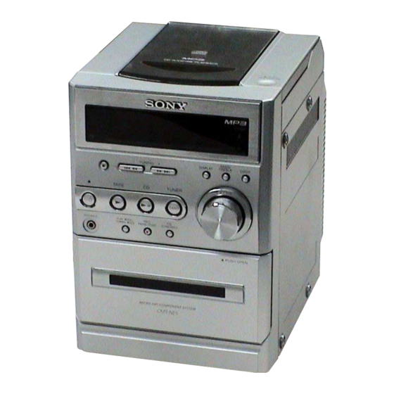
HCD-NE5 is the amplifier, CD player, tape
deck and tuner section in CMT-NE5.
Main unit
Amplifier section
North American model:
Continuous RMS power output (reference):
20 + 20 W (6 ohms at
1 kHz, 10% THD)
European model:
DIN power output (rated): 16 + 16 W (6 ohms at 1
kHz, DIN)
Continuous RMS power output (reference):
20 + 20 W (6 ohms at 1
kHz, 10% THD)
Music power output (reference):
33 + 33 W
Other models:
The following measured at AC 230 V or AC 120 V,
50/60 Hz
DIN power output (rated): 16 + 16 W
(6 ohms at 1 kHz, DIN)
Continuous RMS power output (reference):
20 + 20 W (6 ohms at
1 kHz, 10% THD)
Inputs
MD (phono jacks):
Sensitivity 450 mV,
impedance 47 kilohms
Outputs
PHONES:
Accepts headphones
with an impedance of
8 ohms or more
SPEAKER:
Accepts impedance of
6 to 16 ohms.
CD player section
Laser
Semiconductor laser
( =780 nm)
Emission duration:
continuous
Frequency response
20 Hz 20 kHz
Wavelength
780 790 nm
Sony Corporation
9-877-623-02
2004I05-1
Personal Audio Company
© 2004.09
Published by Sony Engineering Corporation
Model Name Using Similar Mechanism
CD Section
Base Unit Name
Optical Pick-up Name
Model Name Using Similar Mechanism
TAPE Section
Tape Transport Mechanism Type
SPECIFICATIONS
T
ape deck section
Recording system
4-track 2-channel, stereo
Frequency response
50 13,000 Hz ( 3 dB),
using Sony TYPE I
cassettes
Tuner section
FM stereo, FM/AM superheterodyne tuner
FM tuner section
Tuning range
87.5
108.0 MHz
Antenna
FM lead antenna
Antenna terminals
75 ohms unbalanced
Intermediate frequency
10.7 MHz
AM tuner section
Pan-American model:
530 1,710 kHz
(with the tuning interval
set at 10 kHz)
531 1,710 kHz
(with the tuning interval
set at 9 kHz)
European model:
531 1,602 kHz
(with the tuning interval
set at 9 kHz)
Other models:
530 1,710 kHz
(with the tuning interval
set at 10 kHz)
531 1,602 kHz
(with the tuning interval
set at 9 kHz)
Antenna
AM loop antenna,
external antenna terminal
Intermediate frequency
450 kHz
COMPACT DISC DECK RECEIVER
HCD-NE5
Canadian Model
Australian Model
NEW
BU-K7BD81B
KSM-213EDP
NEW
CMAL5Z220A
General
Power requirements
North American model:
120 V AC, 60 Hz
Mexican model:
120 V AC, 60 Hz
European model:
230 V AC, 50/60 Hz
Australian model:
230
50/60 Hz
Korean model:
220 V AC, 60 Hz
Taiwanese model:
120 V AC, 50/60 Hz
Other models:
110 120 V or
220 240 V
AC, 50/60 Hz
Adjustable with voltage
selector
Power consumption
North American model:
50 W
Mexican model:
50 W
European model:
57 W
0.3 W (in Power Saving
Mode)
Korean model:
58 W
Taiwanese model:
50 W
Other models:
65 W
Dimensions (w/h/d)
Approx. 164 230.5 263
mm incl. projecting parts
and controls
Mass
Approx. 3.9 kg
Supplied accessories
Remote Commander (1)
R6 (size AA) batteries (2)
AM loop antenna (1)
FM lead antenna (1)
Design and specifications are subject to change
without notice.
AEP Model
UK Model
E Model
240 V AC,
Advertisement
Table of Contents

Related Manuals for Sony HCD-NE5


Summary of Contents for Sony HCD-NE5
-
Page 1: Specifications
Canadian Model AEP Model Ver 1.1 2004.09 UK Model E Model Australian Model HCD-NE5 is the amplifier, CD player, tape deck and tuner section in CMT-NE5. Model Name Using Similar Mechanism CD Section Base Unit Name BU-K7BD81B Optical Pick-up Name... -
Page 2: Leakage Test
OPERATION. REPLACE THESE COMPONENTS WITH DE FONCTIONNEMENT. NE REMPLACER CES COM- SONY PARTS WHOSE PART NUMBERS APPEAR AS POSANTS QUE PAR DES PIÈCES SONY DONT LES SHOWN IN THIS MANUAL OR IN SUPPLEMENTS PUB- NUMÉROS SONT DONNÉS DANS CE MANUEL OU LISHED BY SONY. -
Page 3: Table Of Contents
HCD-NE5 TABLE OF CONTENTS SERVICING NOTES ..........4 GENERAL Location of Controls ............6 DISASSEMBLY 3-1. Disassembly Flow ............7 3-2. Rear Cabinet ..............7 3-3. Top Panel Assy ..............8 3-4. Front Panel Assy ............. 8 3-5. Base Unit (BU-K7BD81B) ..........9 3-6. -
Page 4: Servicing Notes
HCD-NE5 SECTION 1 SERVICING NOTES • MODEL IDENTIFICATION NOTES ON HANDLING THE OPTICAL PICK-UP – Rear Cabinet – BLOCK OR BASE UNIT The laser diode in the optical pick-up block may suffer electro- static break-down because of the potential difference generated by the charged electrostatic load, etc. - Page 5 HCD-NE5 SERVICE POSITION – CD board – CD board – TCM block – TCM block – AMP board – AMP board...
-
Page 6: General
HCD-NE5 SECTION 2 This section is extracted from instruction manual. GENERAL • LOCATION OF CONTROLS Main unit ALPHABETICAL ORDER 1 2 3 4 5 P - Z A - O PHONES jack qk ALBUM +/ 7 (10, 11) PLAY MODE qj... -
Page 7: Disassembly
HCD-NE5 SECTION 3 DISASSEMBLY • This set can be disassembled in the order shown below. 3-1. DISASSEMBLY FLOW 3-2. REAR CABINET (Page 7) 3-3. TOP PANEL ASSY (Page 8) 3-4. FRONT PANEL ASSY 3-5. BASE UNIT (Page 8) (BU-K7BD81B) (Page 9) 3-6. -
Page 8: Top Panel Assy
HCD-NE5 3-3. TOP PANEL ASSY 6 top panel assy 5 connector (S820) 4 wire (flat type) (27 core) (CN305) 2 claw 1 claw 3-4. FRONT PANEL ASSY 2 wire (flat type) (16 core) (CN303) q; wire (flat type) (15 core) -
Page 9: Base Unit (Bu-K7Bd81B)
HCD-NE5 3-5. BASE UNIT (BU-K7BD81B) 8 base unit (BU-K7BD81B) 5 two washers 7 two washers 4 two screws 6 two screws 3 wire (flat type) (27core) (CN201) 2 CD cover 1 three screws (BTP2.6 3-6. MECHANICAL DECK 1 four screws... -
Page 10: Main Board
HCD-NE5 3-7. MAIN BOARD 8 main board 6 Remove the solder. 1 connector (CN307) 4 two screws 2 connector (CN308) (BVTP3 7 tuner (FM/AM) 3 connector (CN903) 3-8. AMP BOARD 1 connector 2 connector (CN307) (CN308) 4 AMP board 3 two screws... -
Page 11: Test Mode
When observing the eye pattern, set the oscilloscope (In this case, North-American model) for AC range and raise vertical sensitivity. model name (In this case, HCD-NE5) Checking Location: – CD BOARD (Conductor Side) – 5. To exit from this mode, perform the “COLD RESET”. - Page 12 HCD-NE5 MEMO...
-
Page 13: Diagrams
HCD-NE5 SECTION 6 DIAGRAMS 6-1. BLOCK DIAGRAM – CD SERVO Section – FILTER XTSL CD DSP XTAO IC101 (1/2) CLOCK X171 51 53 50 52 DETECTOR XTAI D +3.3V GENERATOR 16.9344MHz XTACN RFACO RFACI AOUT1 RFAC ASYMMETRY SUMMING (Page 14) -
Page 14: Block Diagram - Main Section
HCD-NE5 6-2. BLOCK DIAGRAM – MAIN Section – J303 19 AUX-L R-CH OUT-L POWER J301 PHONES IC501 (Page 13) 21 CD-L R-CH • R-ch is omitted due to same as L-ch. FM/AM TUNER PACK • SIGNAL PATH FM 75 FM ANT... -
Page 15: Note For Printed Wiring Boards And Schematic Diagrams
HCD-NE5 6-3. NOTE FOR PRINTED WIRING BOARDS AND SCHEMATIC DIAGRAMS • Circuit Boards Location Note on Printed Wiring Board: Note on Schematic Diagram: • X : parts extracted from the component side. • All capacitors are in F unless otherwise noted. pF:... -
Page 16: Printed Wiring Board - Cd Board
HCD-NE5 6-4. PRINTED WIRING BOARD – CD Board – • See page 15 for Circuit Boards Location. :Uses unleaded solder. CD BOARD (COMPONENT SIDE) M101 (SPINDLE) CD BOARD (CONDUCTOR SIDE) C302 IC303 S101 (LIMIT) C305 C303 C255 R404 C260 R313... -
Page 17: Schematic Diagram - Cd Board
HCD-NE5 6-5. SCHEMATIC DIAGRAM – CD Board – • • See page 18 for Waveforms. See page 28 for IC Block Diagrams. C131 100p TP423 IOP1 C142 1500p C134 C125 R131 R121 R143 C151 TP10 R203 C143 3.3k TP424 100k... - Page 18 HCD-NE5 • Waveforms – CD Board – – MAIN Board – – CONTROL Board – 1 IC101 yd (LRCK) qa IC301 4 (REC mode) wa IC801 qd (O-XT2) 3.2 Vp-p 4.4 Vp-p 90.4 Vp-p 30.6 s 11.9 s 22.8 s...
-
Page 19: Printed Wiring Board - Main Board
HCD-NE5 6-6. PRINTED WIRING BOARD – MAIN Board – • :Uses unleaded solder. See page 15 for Circuit Boards Location. (Page 22) (Page 24) (Page 16) CD BOARD CONTROL BOARD AMP BOARD CN201 CNB303 CN308 MAIN BOARD J303 S D G... -
Page 20: Schematic Diagram - Main Board (1/2)
HCD-NE5 6-7. SCHEMATIC DIAGRAM – MAIN Board (1/2) – • • See page 18 for Waveforms. See page 28 for IC Block Diagrams. R236 (1/2) J303 R237 C227 R225 C232 1.2k 470p FB302 R125 C132 R226 C236 C394 R137 C127... -
Page 21: Schematic Diagram - Main Board (2/2)
HCD-NE5 6-8. SCHEMATIC DIAGRAM – MAIN Board (2/2) – (2/2) SP OUT L+ J302 C119 L101 1000p GND L- SPEAKER IMPEDANCE GND R- FAN - USE 6-16 Q349,350 R371 VM 10V FAN MOTOR SP OUT R+ R372 DRIVE L201 C219... -
Page 22: Printed Wiring Board - Amp Section
HCD-NE5 6-9. PRINTED WIRING BOARD – AMP Section – • See page 15 for Circuit Boards Location. :Uses unleaded solder. MAIN BOARD MAIN BOARD (Page 19) (Page 19) CNB307 CNB308 AMP BOARD HP BOARD CNB501 FB501 D502 FB502 C525 JW520... -
Page 23: Schematic Diagram - Amp Section
HCD-NE5 6-10. SCHEMATIC DIAGRAM – AMP Section – CN308 R518 C520 2200p FB501 PROTECT CN501 CNB501 R514 C521 2200p AMP-STBY R520 R507 SP O/L SP O/L JW521 AMP-MUTE HP O/L HP O/L R525 J301 PHONES R519 (Page 21) HP O/R... -
Page 24: Printed Wiring Board - Control Board
HCD-NE5 6-11. PRINTED WIRING BOARD – CONTROL Board – • See page 15 for Circuit Boards Location. :Uses unleaded solder. • Semiconductor Location Ref. No. Location CONTROL BOARD S820 CD LID D803 OPEN/CLOSE D807 DETECT D808 D809 D810 D811 D812... -
Page 25: Schematic Diagram - Control Board
HCD-NE5 6-12. SCHEMATIC DIAGRAM – CONTROL Board – • • See page 18 for Waveforms. See page 31 for IC Pin Function Description. FL801 FLUORESCENT INDICATOR TUBE REMOTE CONTROL RECEIVER S820 IC802 (CD LID OPEN/CLOSE DETECT) R881 RPM7240-H4 CN804 R883... -
Page 26: Printed Wiring Board - Power Board
HCD-NE5 6-13. PRINTED WIRING BOARD – POWER Board – • See page 15 for Circuit Boards Location. :Uses unleaded solder. • Semiconductor Location Ref. No. Location (Page 19) (Page 19) (AC IN) MAIN BOARD MAIN BOARD D905 CNB903A CNB903B D906... -
Page 27: Schematic Diagram - Power Board
HCD-NE5 6-14. SCHEMATIC DIAGRAM – POWER Board – JW906 T902 MAIN POWER TRANSFORMER C907 D918 D916 C905 0.022 IN5401 IN5401 0.022 F903 (E,E51,SP,MX,TW,AR,KR,AUS) JW904 F902 C908 D919 D917 C906 0.022 IN5401 IN5401 0.022 CN903 JW905 (MX,TW,AR,KR,AUS) F904 S901 D920 R901... - Page 28 HCD-NE5 • IC Block Diagrams – CD Board – IC101 CXD3059AR IC251 BA5947FM 119 118 115 114 112 111 110 109 103 102 101 100 CPU INTERFACE MUTING SERVO INTERFACE + – 90 RMUT INTERFACE 89 IOVDD0 88 NC LEVEL SHIFT...
- Page 29 HCD-NE5 IC301 TC94A34FG-002 Timing Generator VDDP PO5/AD5 /RESET PO6/AD6 STANDBY PO7AD7 /MICS /MILP MIDIO AD10 VDDT /MICK /MIACK/ SRMSTB AD16 VDDT VDDM PO8/AD11 SDO0 PO9/AD12 /CCE/ PO10/ BCKO AD13 BUCK/ PO11/ LRCKO AD14 SDO3/ SDI0 Interrupt Timer Control Switch General...
- Page 30 HCD-NE5 IC303 BH15FB1WG THERMAL PROTECTION OVER CURRENT PROTECTION VOLTAGE CONTROL REFERENCE BLOCK – MAIN Board – IC302 BD3881FV BASS BASS VOLUME TREBLE LOGIC CONTROL VOLUME TREBLE...
- Page 31 HCD-NE5 IC Pin Function Description CONTROL BOARD IC801 LC876980B-52T3-E (SYSTEM CONTROLLER) Pin No. Pin Name Description MI-ACK Acknowledge signal input from the MP3 decoder MP3-RST Reset signal output to the MP3 decoder MP3-REQ Request signal input from the MP3 decoder...
- Page 32 HCD-NE5 Pin No. Pin Name Description TA END SW END switch signal input from the tape mechanism deck TA PLAY SW PLAY switch signal input from the tape mechanism deck — Not used TU STEREO FM stereo detection signal input from the FM/AM tuner unit...
-
Page 33: Exploded Views
HCD-NE5 SECTION 7 EXPLODED VIEWS NOTE: The components identified by mark • -XX and -X mean standardized parts, so they • Items marked “*” are not stocked since they 0 or dotted line with mark 0 are may have some difference from the original are seldom required for routine service. -
Page 34: Front Panel Assy-1
HCD-NE5 Ver 1.1 7-2. FRONT PANEL ASSY-1 not supplied not supplied not supplied not supplied not supplied not supplied (HP board) not supplied front panel assy-2 Ref. No. Part No. Description Remark Ref. No. Part No. Description Remark 4-253-222-01 KNOB, VOLUME... -
Page 35: Front Panel Assy-2
HCD-NE5 7-3. FRONT PANEL ASSY-2 not supplied not supplied not supplied not supplied not supplied Ref. No. Part No. Description Remark Ref. No. Part No. Description Remark X-4956-282-1 LID, CASS ASSY (X) X-4956-480-1 FRONT PANEL ASSY (X) 4-254-959-01 SPRING, CASSETTE... -
Page 36: Top Panel Assy
HCD-NE5 Ver 1.1 7-4. TOP PANEL ASSY not supplied S820 not supplied S101 The components identified by Les composants identifiés par une mark 0 or dotted line with marque 0 sont critiques pour la mark 0 are critical for safety. -
Page 37: Electrical Parts List
HCD-NE5 SECTION 8 ELECTRICAL PARTS LIST NOTE: • Due to standardization, replacements in the • Items marked “*” are not stocked since they The components identified by mark 0 or dotted line with mark 0 are parts list may be different from the parts speci- are seldom required for routine service. - Page 38 HCD-NE5 Ref. No. Part No. Description Remark Ref. No. Part No. Description Remark C172 1-162-920-11 CERAMIC CHIP 27PF < TRANSISTOR > C174 1-164-360-11 CERAMIC CHIP 0.1uF 6-550-363-01 TRANSISTOR 2SB1690KT146 C181 1-164-360-11 CERAMIC CHIP 0.1uF C182 1-164-360-11 CERAMIC CHIP 0.1uF < RESISTOR >...
- Page 39 HCD-NE5 CONTROL Ref. No. Part No. Description Remark Ref. No. Part No. Description Remark R410 1-216-809-11 METAL CHIP 1/10W D810 8-719-991-33 DIODE 1SS133T-77 R411 1-216-809-11 METAL CHIP 1/10W D811 8-719-062-11 LED SEL2215S-CD (STANDBY) R412 1-216-809-11 METAL CHIP 1/10W D812 8-719-991-33 DIODE 1SS133T-77...
- Page 40 HCD-NE5 CONTROL Ref. No. Part No. Description Remark Ref. No. Part No. Description Remark R814 1-216-852-11 METAL CHIP 390K 1/10W R872 1-216-845-11 METAL CHIP 100K 1/10W R815 1-216-845-11 METAL CHIP 100K 1/10W R874 1-216-833-11 METAL CHIP 1/10W R816 1-216-809-11 METAL CHIP...
- Page 41 HCD-NE5 CONTROL MAIN Ref. No. Part No. Description Remark Ref. No. Part No. Description Remark < VARIABLE RESISTOR > C106 1-162-995-11 CERAMIC CHIP 0.022uF RV801 1-418-632-11 ENCODER, ROTARY (12 TYPE) (VOLUME) C107 1-126-961-11 ELECT 2.2uF C108 1-162-967-11 CERAMIC CHIP 0.0033uF 10% <...
- Page 42 HCD-NE5 MAIN Ref. No. Part No. Description Remark Ref. No. Part No. Description Remark C329 1-126-933-11 ELECT 100uF D311 8-719-109-66 DIODE RD3.3ESB2 C330 1-126-923-91 ELECT 220uF D312 8-719-063-79 DIODE 1N4002B C331 1-162-974-11 CERAMIC CHIP 0.01uF D313 8-719-063-79 DIODE 1N4002B C332...
- Page 43 HCD-NE5 MAIN Ref. No. Part No. Description Remark Ref. No. Part No. Description Remark Q337 8-729-037-03 TRANSISTOR KTA1266GR-AT R214 1-216-818-11 METAL CHIP 1/10W R215 1-216-827-11 METAL CHIP 3.3K 1/10W Q338 8-729-054-16 TRANSISTOR KRC402-RTK R216 1-216-832-11 METAL CHIP 8.2K 1/10W Q342...
- Page 44 HCD-NE5 Ver 1.1 MAIN POWER Ref. No. Part No. Description Remark Ref. No. Part No. Description Remark 0 R361 1-219-787-17 FUSIBLE 1/4W F D910 8-719-991-33 DIODE 1SS133T-77 R362 1-216-836-11 METAL CHIP 1/10W D911 8-719-063-79 DIODE 1N4002B D912 8-719-063-79 DIODE 1N4002B...
- Page 45 HCD-NE5 Ver 1.1 Ref. No. Part No. Description Remark Ref. No. Part No. Description Remark 1-769-953-11 WIRE (FLAT TYPE) (11 CORE) (EXCEPT AEP, UK) 1-829-767-11 WIRE (FLAT TYPE) (15 CORE) (AEP, UK) 1-769-881-11 WIRE (FLAT TYPE) (7 CORE) 1-829-769-11 WIRE (FLAT TYPE) (16 CORE)
-
Page 46: Revision History
HCD-NE5 REVISION HISTORY Clicking the version allows you to jump to the revised page. Also, clicking the version at the upper right on the revised page allows you to jump to the next revised page. Ver. Date Description of Revision 2004.03...