Table of Contents
Advertisement
Quick Links
SERVICE MANUAL
Ver. 1.3 2009.12
HCD-C7NT is the Amplifier, CD player,
MD Deck and Tuner section in CMT-C7NT.
Amplifier section
European model:
DIN power output (rated): 15 + 15 W
(6 ohms at 1 kHz, DIN)
Continuous RMS power output (reference):
20 + 20 W
(6 ohms at 1 kHz, 10%
THD)
Music power output (reference):
45 + 45 W
Other models:
The following measured at 220 V AC, 60 Hz
DIN power output (rated): 15 + 15 W
(6 ohms at 1 kHz, DIN)
Continuous RMS power output (reference):
20 + 20 W
(6 ohms at 1 kHz, 10%
THD)
Inputs
TAPE IN (stereo minijack):
Sensitivity 250 mV,
impedance 47 kilohms
DIGITAL OPTICAL IN (Supported sampling
frequencies: 32 kHz, 44.1 kHz and 48 kHz)
Outputs
TAPE OUT (stereo minijack):
Sensitivity 250 mV,
impedance 1 kilohm
PHONES (stereo minijack):
Accepts headphones with
an impedance of 8 ohms
or more
Sony Corporation
9-873-685-04
2009L05-1
Audio&Video Business Group
© 2009.12
Published by Sony Techno Create Corporation
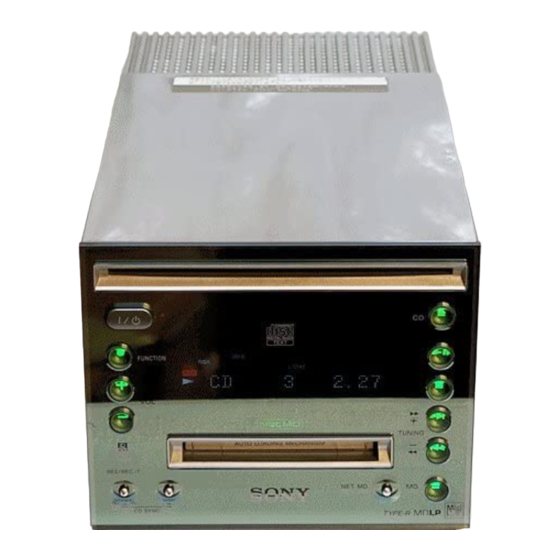
HCD-C7NT
HCD-C7NT
Model Name Using Similar Mechanism
CD
CD Mechanism Type
Section
Base Unit Name
Optical Pick-up Name
Model Name Using Similar Mechanism
MD
MD Mechanism Type
Section
Optical Pick-up Name
SPECIFICATIONS
CD player section
System
Compact disc and digital
audio system
Laser
Semiconductor laser
(λ = 780 nm)
Emission
duration: continuous
Frequency response
2 Hz – 20 kHz
MD deck section
System
MiniDisc digital audio
system
Laser
Semiconductor laser
(λ=780 nm)
Emission duration:
continuous
Sampling frequency
44.1 kHz
Frequency response
5 Hz – 20 kHz
Tuner section
FM stereo, FM/AM superheterodyne tuner
FM tuner section
Tuning range
87.5 – 108.0 MHz
(50-kHz step)
Antenna
FM wire antenna
Antenna terminals
75 ohm unbalanced
Intermediate frequency
10.7 MHz
AM tuner section
Tuning range
European model:
531 – 1,602 kHz
(with the tuning interval
set at 9 kHz)
Other models:
530 – 1,710 kHz
(with the tuning interval
set at 10 kHz)
531 – 1,602 kHz
(with the tuning interval
set at 9 kHz)
Antenna
AM loop antenna, external
antenna terminal
Intermediate frequency
450 kHz
MICRO HI-FI COMPONENT SYSTEM
AEP Model
UK Model
E Model
HCD-C5
TN-CCD1001Z
TT BASE ASSY
OPTIMA-720L1E
New
MDM-7X2B
KMS-262E
General
Power requirements
European model:
230 V AC, 50/60 Hz
Other models:
220 V AC , 50/60 Hz
Power consumption
European model:
See the nameplate
0.5 W (at the power
saving mode)
Other models:
See the nameplate
Approx. 145 × 125 ×
Dimensions (w/h/d)
273 mm incl. projecting
parts and controls
Mass
Approx. 4.5 kg
Supplied accessories
Remote commander (1)
FM wire antenna (1)
AM loop antenna (1)
USB cable (1)
Operating Instructions (1)
M-crew for CMT-C7NT/
OpenMG Jukebox for Net
MD CD-ROM (1)
M-crew Operating
Instructions (1)
OpenMG Jukebox for Net
MD Operating
Instructions (1)
Warranty (1)
Design and specifications are subject to change
without notice.
Advertisement
Table of Contents

Related Manuals for Sony HCD-C7NT


Summary of Contents for Sony HCD-C7NT
- Page 1 HCD-C7NT HCD-C7NT SERVICE MANUAL AEP Model UK Model Ver. 1.3 2009.12 E Model HCD-C7NT is the Amplifier, CD player, MD Deck and Tuner section in CMT-C7NT. Model Name Using Similar Mechanism HCD-C5 CD Mechanism Type TN-CCD1001Z Section Base Unit Name...
-
Page 2: Self-Diagnosis Function
The sound source is a copy of a commercially refer to the following list. If any problem available music software, or you tried to record a persists, consult your nearest Sony dealer. CD-R (Recordable CD) or CD-RW (ReWritable CD). c The Serial Copy Management System prevents making a digital copy (see page 57). -
Page 3: Table Of Contents
HCD-C7NT TABLE OF CONTENTS SELF-DIAGNOSIS FUNCTION ........2 SERVICING NOTES ..........4 GENERAL ..............7 DISASSEMBLY ............9 TEST MODE ............... 24 ELECTRICAL ADJUSTMENTS CD Section ..............33 MD Section ..............34 DIAGRAMS 6-1. Note For Printed Wiring Boards and Schematic Diagrams ............ -
Page 4: Servicing Notes
LIST ARE CRITICAL TO SAFE OPERATION. REPLACE THESE circuit board (within 3 times). COMPONENTS WITH SONY PARTS WHOSE PART NUMBERS • Be careful not to apply force on the conductor when soldering APPEAR AS SHOWN IN THIS MANUAL OR IN SUPPLEMENTS or unsoldering. - Page 5 HCD-C7NT SERVICE POSITION OF THE CD MECHANISM DECK CD MECHANISM DECK (TN-CCD1001Z) UCOM BOARD BD (CD) BOARD CN101 STAND CN204 SERVICE POSITION OF THE MD MECHANISM DECK UCOM BOARD CN203 CN222 BD (CD) BOARD CN204 CN101 CN201 CN102 CN1005 PANEL BOARD...
- Page 6 HCD-C7NT JIG FOR CHECKING BD (MD) BOARD WAVEFORM The special jig (J-2501-196-A) is useful for checking the waveform of the BD (MD) board. The names of terminals and the checking items to be performed are shown as follows. I+3V : For measuring Iop (Check the deterioration of the optical pick-up laser)
-
Page 7: General
HCD-C7NT SECTION 2 This section is extracted GENERAL from instruction manual. Main unit CD SYNC HIGH 8 (19, 60) BUTTON DESCRIPTIONS CD SYNC NORMAL 9 (19) (power) 1 (7, 19, 29, 43, 46, CD Z 2 (10, 60) 48, 53) FUNCTION qs (9, 11, 13, 14, 16, u 3 (9–11, 14–16, 19–21, 26,... - Page 8 HCD-C7NT Remote control qlqk qjqh CD x qh (10, 11) MD x qh (15, 16, 20–22, 26, 28, BUTTON DESCRIPTIONS CD X ws (10) (power) 4 (7, 19, 29, 43, 46, MD X ws (15, 26) CD N wd (9, 11, 21)
-
Page 9: Disassembly
HCD-C7NT SECTION 3 DISASSEMBLY • This set can be disassembled in the order shown below. →) prompts you to move to the next job when all of the works within the dotted square ( • The dotted square with arrow ( ) are completed. - Page 10 HCD-C7NT Note: Follow the disassembly procedure in the numerical order given. 3-1. Bottom Plate, Case 6 case 5 claw 4 screw (+BVTT 3 x 5) 3 bottom plate 2 three screws (+BVTT 3 x 5) 1 four screws (+BVTT 3 x 5) 3-2.
- Page 11 HCD-C7NT 3-3. CD Mechanism Deck (TN-CCD1001Z), BD (CD) Board qs cushion (A) qd CD mechanism deck (TN-CCD1001Z) 7 board to board connector q; screw (+BVTT 2 x 5) qa bracket (CD), foot (felt) 9 two screws (+BVTT 2.6 x 5)
- Page 12 HCD-C7NT 3-4. CONNECTOR Board 1 Remove solderings starting from the left LOADING (+), (–), red and black. 3 Remove solderings starting from the top left SPINDLE (+), (–), FD MOTOR (+), (–) and the LIMIT switch that has no polarity.
- Page 13 HCD-C7NT 3-5. Front Bracket Section, Loading Motor Assy (M902) 8 Remove it in the direction of the arrow A from the left side when viewed from the rear of the front bracket. 7 screw 5 Remove the two (M 2 x 4) 2 screw hang-up springs (FZ).
- Page 14 HCD-C7NT 3-6. SW Board 3 SW board 2 Release it from 1 eleven claws the detents. 5 switch (S3) (Disc Existence, Chucking, Releasing detect) 4 Remove two solderings. (BRN) qd SW board (RED) (ORG) 8 Remove two solderings. (YEL) (GRN) 6 Remove two solderings.
- Page 15 HCD-C7NT 3-7. Feed Motor Assy (M903) 7 feed motor assy (M903) 1 two screws (+P 2 x 10) 4 pulley gear 6 FD gear bracket 2 Remove two white 5 screw solderings. (+P 2 x 3.0) 3-8. Rear Damper Bracket...
- Page 16 HCD-C7NT 3-9. Optical Pick-up (OPTIMA-720L1E), Screw Guide, Feed Screw Assy, etc. 4 screw (+P 2 x 10) 6 optical pick-up (OPTIMA-720L1E), screw guide, feed screw assy, etc. 2 two screws (+P 2 x 10) 1 pick-up flexible board 5 Slant the CONNECTOR board in the direction of the arrow A .
- Page 17 HCD-C7NT 3-11. Base Section 5 two screws (+P2 x 5) 4 Remove solderings from the damper pins. 1 pick-up flexible 2 Remove the two hang-up board springs (FZ) as shown. 7 Remove the two damper pins toward inside. 6 Move the holder (L) in the direction of the arrow A .
- Page 18 HCD-C7NT 3-12. Spindle Motor Assy (M904) 3 open to direction of the arrow A 2 clip arm spring 4 two screws (+P 1.7 x 2.2) 5 turn table 1 clip arm spring (L) 6 washer 7 spindle motor 8 spindle motor assy (M904) 3-13.
- Page 19 HCD-C7NT 3-14. Tuner Pack, D. C. Fan (M901) Note for re-installation 2 wire (flat type) When installing the tuner pack, insert the three harnesses (11 core or 15 core) connected to CN105 and connected to CN106 and connected to CN108 of the AUDIO board, in between the...
- Page 20 HCD-C7NT 3-16. AUDIO Board, POWER Board, Power Transformer (T900) (1) 6 AUDIO board, POWER boad, power transformer (T900 ), etc. 1 two screws (+BVTT 3 x 5) 5 connector (CN102) 2 screw (+BV 3 x 8) 3 four screws (+BVTT 3 x 5)
- Page 21 HCD-C7NT 3-18. MD Mechanism Deck (MDM-7X2B), MD DIGITAL Board 6 two screws (+BVTT 3 x 5) 3 shield (MD2) 7 MD DIGITAL board 2 two screws (+BVTT 3 x 5) 1 four screws (+BVTT 3 x 5) 9 four screws, step...
- Page 22 HCD-C7NT 3-20. BD (MD) Board 2 Remove two solderings. 1 Remove two solderings. (spindle) (sled) M702 M701 M703 6 flexible board 3 Remove two (CN101) solderings. S102 (loading) 4 Remove three solderings. 7 connector (CN104) 5 two screws (+BP TRI 2 x 6 CZN) 8 BD (MD) board 3-21.
- Page 23 HCD-C7NT 3-22. Over Write Head (HR901) 1 screw (+P 1.7 2 over write head (HR901) 3-23. Optical Pick-Up (KMS-262E) q; optical pick-up (KMS-262E) 8 main shaft 3 screw (+BP TRI 2 6 CZN) 9 flexible board 4 base (BU-A) 5 screw (+KTP 2...
-
Page 24: Test Mode
HCD-C7NT SECTION 4 TEST MODE [Factory Preset Mode] [Key Test Mode] ∗ ∗ This mode clears all data including preset data stored in the Keyboard check. RAM to initial conditions. Excute this mode when returning Procedure: 1. Press the ?/1 button to turn the power on. - Page 25 HCD-C7NT [CD Aging Mode] MD SECTION Procedure: 1. Press the ?/1 button to turn the power on. 2. Press the FUNCTION z button to set the CD function, and Note 1: About “R” insert a disc. As this unit has only a few buttons, some operations require 3.
- Page 26 HCD-C7NT 4. BASIC OPERATIONS OF THE TEST MODE All operations are performed using the . “R” , > “R” , ENTER/YES “R” and MENU/NO “R” . The functions of these buttons are as follows. Function name Function . “R” , > “R”...
- Page 27 HCD-C7NT 5-1. Operating the Continuous Playback Mode 5-2. Operating the Continuous Recording Mode (Use only when performing self-recording/palyback check) 1. Entering the continuous playback mode (1) Set the disc in the unit. (Whichever recordable discs or discs for playback only are available) 1.
- Page 28 HCD-C7NT 6. FUNCTIONS OF OTHER BUTTONS Function Contents Sets continuous playback when this is pressed in the STOP state. When this is pressed during continu- ous playback, playback position moves. Stops continuous playback and continuous recording M “R” The sled moves to the outer circumference only when this is pressed m “R”...
- Page 29 HCD-C7NT Iop DATA RECORDING AND DISPLAY WHEN OPTI- WHEN MEMORY NG IS DISPLAYED CAL PICK-UP AND NON-VOLATILE MEMORY (IC195 If the nonvolatile memory data is abnormal, “E001 MEMORY NG” OF BD (MD) BOARD) ARE REPLACED will be displayed so that the MD deck does not continue opera- tions.
- Page 30 HCD-C7NT CHECKS PRIOR TO PARTS REPLACEMENT AND ADJUSTMENTS IN MD Before performing repairs, perform the following checks to determine the faulty locations up to a certain extent. Details of the procedures are described in “5 Electrical Adjustments”. Criteria for Determination...
- Page 31 HCD-C7NT Fig. 2 Reading the Test Mode Display Fig. 1 Reading the Test Mode Display (During recording and stop) (During playback) @@ ### RTs@@c##e fluorescent indicator tube fluorescent indicator tube @@ : Parts No. (name of area named on TOC)
- Page 32 HCD-C7NT Reading the Retry Cause Display Higher Bit Lower Bits Details Hexadecimal Hexadecimal When 0 When 1 Binary Emphasis OFF Emphasis ON Monaural Stereo This is 2-bit display. Normally 01. 01:Normal audio. Others:Invalid Audio (Normal) Invalid Original Digital copy Copyright...
-
Page 33: Electrical Adjustments Cd Section
HCD-C7NT SECTION 5 ELECTRICAL ADJUSTMENTS Checking Location: CD SECTION – BD (CD) BOARD – Note 1: 1. CD Block is basically designed to operate without adjustment. There- fore, check each item in order given. 2. Use YEDS-18 disc (3-702-101-01) unless otherwise indicated. -
Page 34: Md Section
HCD-C7NT MD SECTION Note 1: About “R” As this unit has only a few buttons, some operations require the use of remote commander buttons. These operations are indicated as “R” in this manual. Example: MENU/NO “R” ...Press the MENU/NO button of the remote commander. - Page 35 HCD-C7NT Adjustment flow • Abbreviation OP: optical pick-up Start After turning off and then on the power, initialize the EEPROM Replace IC195 For details, refer to “WHEN MEMORY NG IS DIS- PLAYED” in Section 4. TEST MODE (See page 29) 7.
- Page 36 HCD-C7NT 2. PRECAUTIONS FOR CHECKING LASER DIODE 4. PRECAUTIONS FOR ADJUSTMENTS EMISSION 1. When replacing the following parts, perform the adjustments and checks with in the order shown in the following table. To check the emission of the laser diode during adjustments, never 2.
- Page 37 HCD-C7NT 5. USING THE CONTINUOUSLY RECORDED DISC Procedure: 1. Set the laser power meter on the objective lens of the optical pick-up. (When it cannot be set properly, press the m “R” button * This disc is used in focus bias adjustment and error rate check.
- Page 38 HCD-C7NT 6-4. Auto Check 6-6. Traverse Check This test mode performs CREC and CPLAY automatically for mainly checking the characteristics of the optical pick-up. To perform Note 1:Data will be erased during MO reading if a recorded disc is this test mode, the laser power must first be checked. Perform Auto used in this adjustment.
- Page 39 HCD-C7NT 9. Press the ENTER/YES “R” button to display “EFB = 6. Press the ENTER/YES “R” button to display “ P”. ”. Then, the optical pick-up moves to the pit area automatically The first four digits indicate the C1 error rate, the two digits and servo is imposed.
- Page 40 HCD-C7NT 7. INITIAL SETTING OF ADJUSTMENT VALUE Procedure: 1. Press the . “R” > “R” button to display “TEMP ADJUST” (C03). Note: Mode which sets the adjustment results recorded in the non-volatile memory 2. Press the ENTER/YES “R” button to select the “TEMP to the initial setting value.
- Page 41 HCD-C7NT 6. Press the . “R” or > “R” button so that the reading The method of identifying the optical pick-up of the laser power meter becomes the specified value, press the (KMS-262A/262E) ENTER/YES “R” button to save it. Pink : KMS-262A KMS-262A 8.2 to 8.6 mW...
- Page 42 HCD-C7NT 11. Press the . “R” or > “R” button until the waveform of Procedure: 1. Connect an oscilloscope to CN105 pin 4 (TE) and CN105 pin the oscilloscope moves closer to the specified value. 6 (VC) on the BD (MD) board.
- Page 43 HCD-C7NT 14. ERROR RATE CHECK 13. FOCUS BIAS ADJUSTMENT 14-1. CD Error Rate Check Procedure: 1. Load the continuously-recorded disc. (Refer to “5. USING Procedure: THE CONTINUOUSLY RECORDED DISC” (See page 37)) 1. Load the check disc (TDYS-1). 2. Press the . “R” or > “R” button to display “CPLAY 2 2.
- Page 44 HCD-C7NT 16. AUTO GAIN CONTROL OUTPUT LEVEL ADJUSTMENT Be sure to perform this adjustment when the optical pick-up is replaced. If the adjustment results becomes “Adjust NG!”, the optical pick-up may be faulty or the servo system circuits may be abnormal.
-
Page 45: Diagrams
HCD-C7NT SECTION 6 DIAGRAMS 6-1. Note For Printed Wiring Boards and Schematic Diagrams • Circuit Boards Location (In addition to this, the necessary note is printed in each block) Note on Printed Wiring Boards: Note on Schematic Diagram: • X : parts extracted from the component side. -
Page 46: Block Diagram - Cd Servo Section
HCD-C7NT 6-2. Block Diagram – CD Servo Section – • Signal Path Q102 SWITCH : CD OPTICAL PICK-UP IC101 BLOCK DIGITAL SERVO, IC103 OPTIMA-720L1E DIGITAL SIGNAL PROCESSOR RF AMP 1/2VCC D OUT D OUT SECTION RFAC RFAC (Page 49) RFDCO... -
Page 47: Block Diagram - Md Servo Section
HCD-C7NT 6-3. Block Diagram – MD Servo Section – SCTX IC151 (1/2) IC181, Q181 182 EFMO ADDT OVER WRITE HEAD DRIVE FILI DADTI DADTI SAMPLING HR901 RATE OVER WRITE HEAD XBCKI XBCKI CONVERTER IC151 (1/2) CLTV LRCKI LRCKI DIGITAL SIGNAL PROCESSOR,... -
Page 48: Block Diagram - Main Section
HCD-C7NT 6-4. Block Diagram – Main Section – REC-L SECTION IC301 (Page 49) SOUND PROCESSOR IC302 DAOUT-L HEADPHONE AMP CD/MD SECTION J103 R-CH (Page 49) PHONES – Q331 Q232 MUTING Q341 DETECT J102 Q311 MUTING D343 R-CH DBFB SWITCH TAPE... -
Page 49: Block Diagram - Usb Section
HCD-C7NT 6-5. Block Diagram – USB section – IC1006 IC222 IC221 AD/DA CONVERTER SELECTOR DIGITAL DIGITAL OPT-IN OPTICAL OPTICAL 2 RX3 DAOUTL MAIN LOUT DOUT SECTION ROUT R-CH SECTION 4 RX4 (Page 48) (Page 46) MAIN REC-L SECTION IC1012 (Page 48) -
Page 50: Printed Wiring Boards - Bd (Cd) Board
HCD-C7NT 6-6. Printed Wiring Boards – BD (CD) Board – • See page 45 for Circuit Boards Location. • Semiconductor Location Ref. No. Location D101 IC101 IC102 IC103 IC1102 IC103 Q101 IC102 Q102 Q103 IC1102 (Page 52) RFAC RVC1.65V (Page 61) -
Page 51: Schematic Diagram - Bd (Cd) Board
HCD-C7NT 6-7. Schematic Diagram – BD (CD) Board – • See page 45 for Wavefoms. • See page 70 for IC Block Diagrams. (Page 53) LOADING MOTOR- LOADING MOTOR+ IC B/D RESET SWITCH SPINDLE MOTOR+ SPINDLE MOTOR- FEED MOTOR+ FEED MOTOR-... -
Page 52: Printed Wiring Boards - Connector Section
HCD-C7NT 6-8. Printed Wiring Boards – Connector Section – • See page 45 for Circuit Boards Location. SW BOARD CONNECTOR BOARD M902 LOADING MOTOR (8cm Disc Eject End Detect) (Disc IN/8cm Disc Detect) (Disc/ Chacking/ Release Detect) (12cm Disc/12cm Disc Eject End Detect) -
Page 53: Schematic Diagram - Connector Section
HCD-C7NT 6-9. Schematic Diagram – Connector Section – S1 (Disc IN/8cm Disc Detect) S2 (12cm Disc/12cm Disc Eject End Detect) S3 (Disc/ Chacking/ Release Detect) S4 (8cm Disc Eject End Detect) (Page 51) LOADING MOTOR- LOADING MOTOR+ RESET SWITCH SPINDLE MOTOR+... -
Page 54: Printed Wiring Board - Bd (Md) Board
HCD-C7NT 6-10. Printed Wiring Board – BD (MD) Board – • See page 45 for Circuit Boards Location. OPTICAL PICK - UP BLOCK BD (MD) BOARD (SIDE A) (KMS-262E) BD (MD) BOARD (SIDE B) • Semiconductor Location Side A Ref. No. Location... -
Page 55: Schematic Diagram - Bd (Md) Board (1/2)
HCD-C7NT 6-11. Schematic Diagram – BD (MD) Board (1/2) – • See page 45 for Wavefoms. • See page 71 for IC Block Diagrams. • See page 74 for IC Pin Function Description. 106-QR (MD) (KMS-262E) (MD) M701 BH6519FS-E2 IC B/D... -
Page 56: Schematic Diagram - Bd (Md) Board (2/2)
HCD-C7NT 6-12. Schematic Diagram – BD (MD) Board (2/2) – • See page 45 for Wavefoms. • See page 75 for IC Pin Function Description. IC195 is a written in and settled EEPROM. Supply with a single article has not been carried out. In case you exchange by BD board (A-4726-972-A), please put on IC195 currently used with the model again. -
Page 57: Printed Wiring Board - Md Digital Board
HCD-C7NT 6-13. Printed Wiring Board – MD DIGITAL Board – • See page 45 for Circuit Boards Location. • Semiconductor Location Ref. No. Location IC1015 IC1012 D1004 D1005 D1006 IC1006 IC1005 D1010 IC1008 D1013 D1014 CN102 D2001 D2002 CN203 (Page 63) -
Page 58: Schematic Diagram - Md Digital Board (1/3)
HCD-C7NT 6-14. Schematic Diagram – MD DIGITAL Board (1/3) – • See page 45 for Wavefoms. • See page 78 for IC Pin Function Description. (Page 56) TE-17 TE-17 TE-17 R1042 10k M30833FJGP-C7N-2 R1041 10k (KR) TE-17 D2006 1SS355TE-17 D2005... -
Page 59: Schematic Diagram - Md Digital Board (2/3)
HCD-C7NT 6-15. Schematic Diagram – MD DIGITAL Board (2/3) – • See page 45 for Wavefoms. • See page 72 for IC Block Diagrams. X1005 12.5MHz USB-I2C CONVERTER PFM-G-310-BND IC B/D MB89595CPFV-G-122-BND (Page 62) -
Page 60: Schematic Diagram - Md Digital Board (3/3)
HCD-C7NT 6-16. Schematic Diagram – MD DIGITAL Board (3/3) – • See page 45 for Wavefoms. • See page 72, 73 for IC Block Diagrams. IC B/D AFEL MD REC-R MD REC-L MD-L (Page 64) MD-R TE-17 TE-17 E/2K E/2K... -
Page 61: Printed Wiring Board - Ucom Board
HCD-C7NT 6-17. Printed Wiring Board – UCOM Board – • See page 45 for Circuit Boards Location. • Semiconductor Location Ref. No. Location Ref. No. Location D214 IC222 D221 IC501 D222 IC941 D513 D910 Q202 D923 Q211 D924 Q212 D925... -
Page 62: Schematic Diagram - Ucom Board
HCD-C7NT 6-18. Schematic Diagram – UCOM Board – • See page 45 for Wavefoms. • See page 80 for IC Pin Function Description. (Page 51) (Page 64) (Page 58) (Page 59) (Page 66) (Page 64) (Page 68) (Page 68) -
Page 63: Printed Wiring Boards - Audio Section
HCD-C7NT 6-19. Printed Wiring Boards – Audio Section – • See page 45 for Circuit Boards Location. • Semiconductor Location Ref. No. Location Ref. No. Location D101 Q101 D102 Q102 D103 Q103 D104 Q104 D105 Q105 D301 Q151 D343 Q311... -
Page 64: Schematic Diagram - Audio Section
HCD-C7NT 6-20. Schematic Diagram – Audio Section – • See page 69 for IC Block Diagrams. (Page 60) 11P (KR) (Page 68) IC B/D (Page 62) (Page 62) -
Page 65: Printed Wiring Board - Panel Board
HCD-C7NT 6-21. Printed Wiring Board – PANEL Board – • See page 45 for Circuit Boards Location. • Semiconductor Location Ref. No. Location D601 D602 D603 D604 D605 D606 D607 D608 D609 D610 D611 D612 IC601 IC601 IC602 Q601 Q602... -
Page 66: Schematic Diagram - Panel Board
HCD-C7NT 6-22. Schematic Diagram – PANEL Board – • See page 71 for IC Block Diagrams. FLUORESCENT INDICATOR TUBE IC B/D SELS5LED23C- STP15 SELS5LED23C- STP15 SELS5LED23C-STP15 SELS5LED23C-STP15 SELS5LED23C-STP15 SELS5LED23C-STP15 SELS5LED23C-STP15 SELS5LED23C-STP15 SELS5LED23C-STP15 SELS5LED23C-STP15 SELS5LED23C-STP15 (Page 62) -
Page 67: Printed Wiring Boards - Power Section
HCD-C7NT 6-23. Printed Wiring Boards – Power Section – • See page 45 for Circuit Boards Location. (Page 61) IC902 (MAIN) IC901 (Page 61) IC908 IC903 IC904 POWER TRANSFORMER(SUB) • Semiconductor Location IC906 Ref. No. Location Ref. No. Location D921... -
Page 68: Schematic Diagram - Power Section
HCD-C7NT 6-24. Schematic Diagram – Power Section – *F851,852 T2.5AL/250V(AEP,UK) 4A/250V(KR) 1/4W (Page 62) R981 TA7805S (Page 64) TA7805S TA7805S (Page 62) TA7805S 1/4W... -
Page 69: Ic Block Diagrams
HCD-C7NT 6-25. IC Block Diagrams IC301 M62428AFP600C (AUDIO BOARD) AVDD VREF REF AMP AGND – VREFI VREFO SUR R SURROUND SW MIC IN AGND SUR C IN1A IN2A IN1B – IN2B IN1C BUFF BUFF AMP1 AMP2 IN2C IN1D IN2D AMP1... - Page 70 HCD-C7NT IC101 CXD3068Q (BD (CD) BOARD) IC103 CXA2581N-T4 (BD (CD) BOARD) RW/ROM DC OFST RFDCI – – RFDCO – RW/ROM VOFST APC AMP EQ ON/OFF RFAC EQ IN RW/ROM RFAC AC SUM SUMMING VOFST – – RW/ROM TE BAL RW/ROM –...
- Page 71 HCD-C7NT IC141 BH6519FS-E2 (BD (MD) BOARD) INTERFACE INTERFACE CHARGE PREDRIVE PREDRIVE PUMP. PREDRIVE PREDRIVE INTERFACE INTERFACE IC601 M66004M8FP-200D (PANEL BOARD) DIG11 DIG12 DIGITAL OUTPUT DIG0 DIG15 CIRCUIT INDICATION CONTROLLER SERIAL RECEIVE CIRCUIT DATA INDICATION OUTPUT CONTROL PORT RESISTOR (2BIT) CLOCK...
- Page 72 HCD-C7NT IC1002 CXD1873R (MD DIGITAL BOARD) 12MHz VDEC0 TEST1 VSEC0 DNK RS RAM 16KB VSC2 CPU CK VDC3 CPU SO RAM 8KB CPU SI DNK ST VDEC1 DNK SI VSEC1 DNK SO CPU XCS VSEA2 CONTROL CPU INT VDEA3 RESET...
- Page 73 HCD-C7NT IC1007 PCM2702E/2K (MD DIGITAL BOARD) SYSTEM CLOCK AUDIO VCCP VDDC CLOCK CLOCK AGNDP DGNDC VCCL AGNDL POWER SUPPLY DGND VOUTL MULTI- VBUS VCOM USB I/F OVER- LEVEL DGNDU AGND SAMPLING DELTA- DIGITAL PLYBCK SIGMA FILTER MODULATOR VOUTR SSPND ZERO...
-
Page 74: Ic Pin Function Description
HCD-C7NT 6-26. IC Pin Function Description • IC101 CXA2523AR RF Amplifier (BD(MD) Board) Pin No. Pin Name Description I-V converted RF signal I input I-V converted RF signal J input Middle point voltage (+1.5V) generation output 4 to 9 A to F... - Page 75 HCD-C7NT • IC151 CXD2662R Digital Signal Processor, Digital Servo Signal Processor (BD(MD) Board) Pin No. Pin Name Description Function FOK signal output to the master controller (monitor output) MNT0 (FOK) “H” is output when focus is on (Not used) MNT1 (SHCK)
- Page 76 HCD-C7NT Pin No. Pin Name Description Data input/output for DRAM 50, 51 D2, D3 MVCI I (S) Clock input from an external VCO (Fixed at “L”) ASYO Playback EFM duplex signal output ASYI I (A) Playback EFM comparator slice level input AVDD —...
- Page 77 HCD-C7NT Pin No. Pin Name Description TFDR Tracking servo drive PWM output (+) to the BH6519FS DVDD — +3V power supply (Digital) FFDR Focus servo drive PWM output (+) to the BH6519FS FRDR Focus servo drive PWM output (–) to the BH6519FS 176.4 kHz clock signal output (X’tal) (Not used)
- Page 78 HCD-C7NT • IC1003 M30835 Master Controller (MD DIGITAL Board) Pin No. Pin Name Description A-IN – Not used – Not used NETMD-SO Serial communication data output to the IC1002 NETMD-SI Serial communication data input from the IC1002 NETMD-CLK Serial clock output to the IC1002...
- Page 79 HCD-C7NT Pin No. Pin Name Description XLAT Latch signal output to the DSP IC Serial clock output to the EEPROM OUT-SW Detection signal input from the loading out detection switch MNT2 Busy monitoring signal input from the mechanism deck MNT1...
- Page 80 HCD-C7NT • IC501 µPD703032AYGY-M02-3BA Master Control (UCOM Board) Pin No. Pin Name Description FL-DATA Data signal output to the fluorescent indicator tube FL-CLK Clock signal output to the fluorescent indicator tube I2C data input/output FL-CE Enable signal output to the fluorescent indicator tube...
- Page 81 HCD-C7NT Pin No. Pin Name Description PROTECT Not used (fixed at “H”) PRE-MUTE Pre-amplifier muting signal output PWR-MUTE Not used (open) REC-MUTE REC muting signal output HP-MUTE Not used (open) SPK-RELAY Speaker relay control signal output HELP I2C busy signal input/output BVDD –...
-
Page 82: Exploded Views
HCD-C7NT SECTION 7 EXPLODED VIEWS NOTE: • -XX, -X mean standardized parts, so they may • The mechanical parts with no reference number The components identified by mark 0 or have some differences from the original one. in the exploded views are not supplied. - Page 83 HCD-C7NT 7-2. Front Panel Section FL601 not supplied not supplied not supplied Ref. No. Part No. Description Remarks Ref. No. Part No. Description Remarks X-4954-278-2 FRONT PANEL ASSY A-4727-470-A PANEL BOARD, COMPLETE 4-228-335-11 LID (MD) 4-233-850-01 HOLDER (FL) 4-233-846-14 ESCUTCHEON (MD)
- Page 84 HCD-C7NT 7-3. Chassis Section-1 F852 F851 M901 supplied T900 chassis section -2 Ref. No. Part No. Description Remarks Ref. No. Part No. Description Remarks A-4727-467-A UCOM BOARD, COMPLETE (AEP, UK) 3-701-748-00 CLAMP A-4727-481-A UCOM BOARD, COMPLETE (KR) 4-812-134-31 RIVET (DIA. 3.5), NYLON...
- Page 85 HCD-C7NT 7-4. Chassis Section-2 not supplied not supplied not supplied MD mechanism deck section -1 (MDM-7X2B) not supplied not supplied Ref. No. Part No. Description Remarks Ref. No. Part No. Description Remarks 4-231-555-01 INSULATOR A-4727-479-A MD DIGITAL BOARD, COMPLETE 4-228-643-21 SCREW (+BVTTWH M3), STEP 1-823-773-11 WIRE (FLAT TYPE) (23 CORE) 4-231-113-01 SCREW (1.7X3), BTN...
- Page 86 HCD-C7NT 7-5. CD Mechanism Deck Section (TN-CCD1001Z) supplied CD mechanism deck section -chassis section (TN-CCD1001Z) supplied CD mechanism deck section -front bracket section (TN-CCD1001Z) M902 supplied CD mechanism deck section -base section (TN-CCD1001Z) Ref. No. Part No. Description Remarks Ref. No.
- Page 87 HCD-C7NT 7-6. CD Mechanism Deck Section – Front Bracket Section (TN-CCD1001Z) not supplied not supplied not supplied Ref. No. Part No. Description Remarks Ref. No. Part No. Description Remarks 4-236-112-01 SPRING (R), LOADING PULLEY 4-236-118-01 WASHER (117) 4-236-115-01 BRACKET (J), FRONT...
- Page 88 HCD-C7NT 7-7. CD Mechanism Deck Section – Base Section (TN-CCD1001Z) supplied supplied supplied M903 M904 Ref. No. Part No. Description Remarks Ref. No. Part No. Description Remarks X-4954-022-1 SCREW ASSY, FEED 4-236-090-01 BASE, FM 4-236-104-01 SPRING, PULLEY GUIDE 4-236-091-01 BRACKET, FD GEAR...
- Page 89 HCD-C7NT 7-8. CD Mechanism Deck Section – Chassis Section (TN-CCD1001Z) supplied Ref. No. Part No. Description Remarks Ref. No. Part No. Description Remarks 4-236-085-01 ARM, SLIDE 4-236-079-01 ARM (L), HOLDER 4-236-086-01 SPRING, SLIDE ARM 4-236-077-01 SPRING, TRIGGER 4-236-073-01 ARM (R), S...
- Page 90 HCD-C7NT Ver. 1.3 7-9. MD Mechanism Deck Section-1 (MDM-7X2B) not supplied supplied not supplied MD mechanism deck section -2 (MDM-7X2B) Ref. No. Part No. Description Remarks Ref. No. Part No. Description Remarks * 701 4-996-267-01 BASE (BU-D) 4-226-996-01 LIMITTER (EJ)
- Page 91 HCD-C7NT Ver. 1.3 7-10. MD Mechanism Deck Section-2 (MDM-7X2B) HR901 S102 M701 M702 M703 Ref. No. Part No. Description Remarks Ref. No. Part No. Description Remarks 4-231-319-01 SCREW (2X6) CZN, +B (P) TRI 4-226-992-01 BASE, SL 3-372-761-01 SCREW (M1.7), TAPPING...
-
Page 92: Electrical Parts List
HCD-C7NT SECTION 8 ELECTRICAL PARTS LIST AMP POWER AUDIO NOTE: • Due to standardization, replacements in the • RESISTORS • Abbreviation parts list may be different from the parts All resistors are in ohms. KR : Korean model specified in the diagrams or the components... - Page 93 HCD-C7NT AUDIO BD (CD) Ref. No. Part No. Description Remarks Ref. No. Part No. Description Remarks * CN105 1-564-518-11 PLUG, CONNECTOR 3P R326 1-218-867-11 RES-CHIP 6.8K 1/10W * CN106 1-568-934-11 PIN, CONNECTOR 7P R327 1-249-433-11 CARBON 1/4W * CN108 1-568-943-11 PIN, CONNECTOR 5P...
- Page 94 HCD-C7NT BD (CD) Ref. No. Part No. Description Remarks Ref. No. Part No. Description Remarks C119 1-115-156-11 CERAMIC CHIP < IC > C120 1-126-513-11 ELECT 47uF 20.00% 6.3V C154 1-164-360-11 CERAMIC CHIP 0.1uF IC101 8-752-408-73 IC CXD3068Q C159 1-162-968-11 CERAMIC CHIP 0.0047uF 10%...
- Page 95 HCD-C7NT BD (CD) BD (MD) Ref. No. Part No. Description Remarks Ref. No. Part No. Description Remarks R207 1-216-857-11 METAL CHIP 1/16W C121 1-164-156-11 CERAMIC CHIP 0.1uF R212 1-216-813-11 METAL CHIP 1/16W C125 1-117-720-11 CERAMIC CHIP 4.7uF R215 1-216-864-11 METAL CHIP...
- Page 96 HCD-C7NT BD (MD) Ref. No. Part No. Description Remarks Ref. No. Part No. Description Remarks < IC > < RESISTOR > IC101 8-752-080-95 IC CXA2523AR R101 1-216-829-11 METAL CHIP 4.7K 1/16W IC102 8-759-473-51 IC TLV2361CDBV R102 1-216-853-11 METAL CHIP 470K...
- Page 97 HCD-C7NT BD (MD) CONNECTOR JACK MD DIGITAL Ref. No. Part No. Description Remarks Ref. No. Part No. Description Remarks R171 1-216-821-11 METAL CHIP 1/16W 1-683-334-13 JACK BOARD R173 1-216-821-11 METAL CHIP 1/16W *********** R174 1-216-811-11 METAL CHIP 1/16W R177 1-216-805-11 METAL CHIP 1/16W <...
- Page 98 HCD-C7NT MD DIGITAL Ref. No. Part No. Description Remarks Ref. No. Part No. Description Remarks C1042 1-164-156-11 CERAMIC CHIP 0.1uF D1014 8-719-210-39 DIODE EC10QS-04-TE12L C1043 1-164-156-11 CERAMIC CHIP 0.1uF D2001 8-719-988-61 DIODE 1SS355TE-17 C1044 1-162-970-11 CERAMIC CHIP 0.01uF D2002 8-719-988-61 DIODE 1SS355TE-17...
- Page 99 HCD-C7NT MD DIGITAL PANEL Ref. No. Part No. Description Remarks Ref. No. Part No. Description Remarks R1009 1-216-864-11 METAL CHIP 1/16W R1080 1-216-833-11 METAL CHIP 1/16W R1010 1-216-864-11 METAL CHIP 1/16W R1081 1-216-864-11 METAL CHIP 1/16W R1012 1-218-874-11 METAL CHIP 0.5%...
- Page 100 HCD-C7NT PANEL Ref. No. Part No. Description Remarks Ref. No. Part No. Description Remarks C635 1-124-247-91 ELECT 10uF 20.00% 35V < RESISTOR > C636 1-126-153-11 ELECT 22uF 6.3V C637 1-164-156-11 CERAMIC CHIP 0.1uF R601 1-249-441-11 CARBON 100K 1/4W C640 1-162-927-11 CERAMIC CHIP...
- Page 101 HCD-C7NT POWER Ref. No. Part No. Description Remarks Ref. No. Part No. Description Remarks A-4727-468-A POWER BOARD, COMPLETE (AEP, UK) D985 8-719-200-82 DIODE 11ES2-TA1B A-4727-482-A POWER BOARD, COMPLETE (KR) D991 8-719-991-33 DIODE 1SS133T-77 D992 8-719-991-33 DIODE 1SS133T-77 *********************** D993 8-719-991-33 DIODE 1SS133T-77 4-363-146-00 HEAT SINK, V.OUT...
- Page 102 HCD-C7NT UCOM Ref. No. Part No. Description Remarks Ref. No. Part No. Description Remarks 1-682-099-11 SW BOARD < CONNECTOR > ********* * CN201 1-784-738-11 CONNECTOR, FFC 16P < SWITCH > CN202 1-784-780-11 CONNECTOR, FFC 19P CN203 1-764-698-11 SOCKET, CONNECTOR (NON ZIF)19P...
- Page 103 HCD-C7NT UCOM Ref. No. Part No. Description Remarks Ref. No. Part No. Description Remarks < JUMPER RESISTOR > R512 1-247-887-00 CARBON 220K 1/4W R513 1-247-807-31 CARBON 1/4W JR200 1-216-864-11 METAL CHIP 1/16W R514 1-247-807-31 CARBON 1/4W JR203 1-216-864-11 METAL CHIP...
- Page 104 HCD-C7NT Ver. 1.3 UCOM Ref. No. Part No. Description Remarks Ref. No. Part No. Description Remarks R578 1-216-821-11 METAL CHIP 1/16W MISCELLANEOUS R579 1-216-821-11 METAL CHIP 1/16W ************** R580 1-216-833-11 METAL CHIP 1/16W R581 1-216-833-11 METAL CHIP 1/16W 1-757-791-11 WIRE (FLAT TYPE) (16 CORE)
- Page 105 HCD-C7NT MEMO...
- Page 106 REVISION HISTORY Clicking the version allows you to jump to the revised page. Also, clicking the version at the top of the revised page allows you to jump to the next revised page. Ver. Date Description of Revision 2002.03 2005.02 Exchange of Parts No.