Table of Contents
Advertisement
Quick Links
Service
Manual
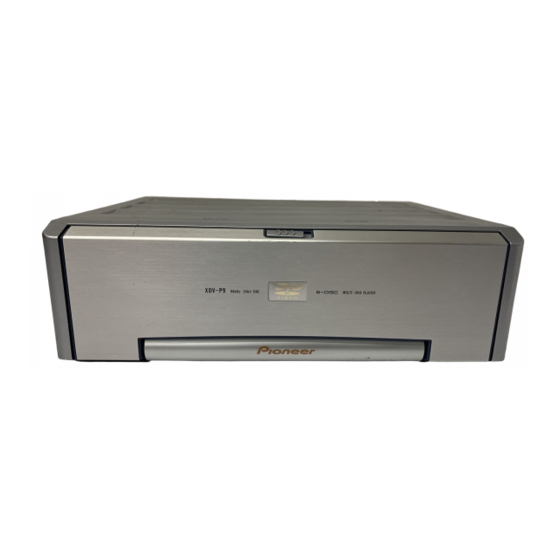
6-DISC MULTI-DVD PLAYER
XDV-P9
- This service manual should be used together with the following manual(s):
Model No.
Order No.
CX-692
CRT2533
- Manufactured under license from Dolby Laboratories. "Dolby" and the double-D symbol are trademarks of Dolby
Laboratories. Confidential unpublished works. © 1992-1997 Dolby Laboratories. All rights reserved.
- Manufactured under license from Digital Theater Systems, Inc. "DTS" and "DTS Digital Surround" are trademarks
of Digital Theater Systems, Inc.
CONTENTS
1. SAFETY INFORMATION ............................................3
2. EXPLODED VIEWS AND PARTS LIST.......................4
4. PCB CONNECTION DIAGRAM ................................40
5. ELECTRICAL PARTS LIST ........................................54
6. ADJUSTMENT..........................................................64
PIONEER CORPORATION
PIONEER ELECTRONICS SERVICE INC.
PIONEER EUROPE NV
Haven 1087 Keetberglaan 1, 9120 Melsele, Belgium
PIONEER ELECTRONICS ASIACENTRE PTE.LTD. 253 Alexandra Road, #04-01, Singapore 159936
C PIONEER CORPORATION 2000
XDV-P9/UC
Mech. Module Remarks
MM-1
DVD/CD Mech. Unit:Circuit Description, Mech.Description, Disassembly
4-1, Meguro 1-Chome, Meguro-ku, Tokyo 153-8654, Japan
P.O.Box 1760, Long Beach, CA 90801-1760 U.S.A.
UC,ES/RC,ES/RD,EW
7. GENERAL INFORMATION .......................................73
7.1 DIAGNOSIS ........................................................73
7.1.1 TEST MODE ..............................................73
7.1.2 DISASSEMBLY .........................................84
7.2 IC ........................................................................88
7.3 OPERATIONAL FLOW CHART.........................111
8. OPERATIONS AND SPECIFICATIONS ..................112
K-ZZD. MAY 2000 Printed in Japan
ORDER NO.
CRT2511
Advertisement
Table of Contents

Related Manuals for Pioneer XDV-P9


Summary of Contents for Pioneer XDV-P9
-
Page 1: Table Of Contents
PIONEER ELECTRONICS SERVICE INC. P.O.Box 1760, Long Beach, CA 90801-1760 U.S.A. PIONEER EUROPE NV Haven 1087 Keetberglaan 1, 9120 Melsele, Belgium PIONEER ELECTRONICS ASIACENTRE PTE.LTD. 253 Alexandra Road, #04-01, Singapore 159936 C PIONEER CORPORATION 2000 K-ZZD. MAY 2000 Printed in Japan... - Page 2 XDV-P9 - DVD Player Service Precautions Never adjust the LD VR in the pickup unit to 3. During disassembly, be sure to turn the power off since an internal IC might be destroyed when a protect the pickup from electrical damages.
-
Page 3: Safety Information
XDV-P9 1. SAFETY INFORMATION 1.1 XDV-P9/UC CAUTION This service manual is intended for qualified service technicians; it is not meant for the casual do-it-yourselfer. Qualified technicians have the necessary test equipment and tools, and have been trained to properly and safely repair complex products such as those covered by this manual. -
Page 4: Exploded Views And Parts List
XDV-P9 2. EXPLODED VIEWS AND PARTS LIST 2.1 PACKING... - Page 5 XDV-P9 NOTE: - Parts marked by “*” are generally unavailable because they are not in our Master Spare Parts List. ∇ mark on the product are used for disassembly. - Screws adjacent to - PACKING SECTION PARTS LIST Part No.
- Page 6 XDV-P9 2.2 EXTERIOR...
- Page 7 XDV-P9 (1) EXTERIOR SECTION PARTS LIST Mark No. Description Part No. Mark No. Description Part No. 1 Screw BMZ30P040FZK 46 Connector(CN302) CKS3480 2 Screw CBA1353 47 Connector(CN1600) CKS3749 3 Spring CBH2354 48 Connector(CN310) CKS3767 4 IC(IC3951) PQ30RV31 49 Connector(CN301) CKS4358...
- Page 8 XDV-P9 (2) CONTRAST TABLE XDV-P9/UC, XDV-P9/ES/RC, XDV-P9/ES/RD and XDV-P9/EW are constructed same except for the following: Part No. Mark No. Description XDV-P9/UC XDV-P9/ES/RC XDV-P9/ES/RD XDV-P9/EW Remote Control Main Assy CPN1638 CPN1639 CPN1639 Not used Case CNS6050 CNS6050 CNS6050 Not used...
- Page 9 XDV-P9 2.3 DVD MECHANISM...
- Page 10 XDV-P9 - DVD MECHANISM SECTION PARTS LIST Mark No. Description Part No. Mark No. Description Part No. 1 Screw CBA1026 46 Lever CNC8097 2 Screw(M2x2.5) CBA1037 47 Bracket CNC8106 3 Screw(M2x2.5) CBA1041 48 Cover CNC8129 4 Screw(M2x3.5) CBA1114 49 Arm...
- Page 11 XDV-P9 Mark No. Description Part No. Mark No. Description Part No. 91 Lever Unit CXB2266 111 Motor(Spindle)(M3) CXM1151 CXB3930 112 Screw IMS26P040FMC Motor Unit(-B)(Carriage)(M1) 93 Screw JFZ20P025FNI 113 Screw JFZ17P020FNI 94 Motor Unit(-C)(ELV)(M4) CXB3931 114 Gear CNV6225 95 Gear CNV6239...
-
Page 12: Block Diagram And Schematic Diagram
XDV-P9 3. BLOCK DIAGRAM AND SCHEMATIC DIAGRAM 3.1 BLOCK DIAGRAM - DVD/CD Mechanism Unit, Main Unit MAIN UNIT Q103 27MMC CN101 Q104 RFO 28 BCK 109 78LD DXTKI LDO1 LRCK 110 BCK 2 CDBCK XI 73 ADATAO 111 78MPD IC 105... - Page 13 XDV-P9 CN1600 DIGOUT DSPCLK AODAI 64 IC 1504 DAC5V HA178L05UA BCK 109 CDBCK CDBCK CDBCK LRCK 110 CDLRCK Q1500 Q1503 CDLRCK CDLR F1500 ANACOMP 45 COMPOUT CDDATA CDDATA ADATAO CDDATA CTF1515 SD0-SD7 IC 1201 IC 1500 IC 1501 IC 1503...
- Page 14 XDV-P9 - Extension Unit, Keyboard Unit EXTENSION UNIT CN3701 DIGO COMP IC 3 NJM20 Q3589 Q3588 Q3586 XAMUTE Q3592 IC 3 PQ30 VDCONT Q3587 Q3951 Q3953 VMCONT XMBSEN VMUTE STEMP STEMP IP-BUS DRIVER Q3962 CN3991 2.6V REGULATOR IC 3961 BA08T...
- Page 15 XDV-P9 CN3801 OUTPUT IC 3801 OPTOUT TC7SHU04FU DDC5 CN3831 FRONTVOUT FRONT VIDEO IC 3721 IC 3722 OUTPUT NJM2267M NJM2267M REARVOUT REAR MONITOR OUTPUT AUDIO MUTE IC 3511 REARLOUT L ch NJM2068MD AUDIO OUTPUT Q3574 Q3572 Q3571 IC 3951 PQ30RV31 Q3573...
- Page 16 XDV-P9 3.2 DVD MECHANISM UNIT, MAIN UNIT(SERVO SECTION)(GUIDE PAGE) Note: When ordering service parts, be sure to refer to “EXPLODED VIEWS AND PARTS LIST” or “ELECTRICAL PARTS LIST”. MAIN UNIT(SERVO SECTION) Large size SCH diagram R(DVD) Guide page R(DVD) R(DVD)
- Page 17 XDV-P9 F.ACT DRIVE RF EQUALIZER T.ACT DRIVE CRG DRIVE SPDL DRIVE AUDIO AUDIO(ANALOG) SIGNAL ROM DATA SIGNAL R(DVD) & R(DVD) LCD DRIVE AUDIO AUDIO 3.3V F JUMP AUDIO DRAM ASIC R(DVD) NOTE : Symbol indicates a resistor. Decimal points for resistor...
- Page 18 XDV-P9...
- Page 19 XDV-P9 A B C D...
- Page 20 XDV-P9...
- Page 21 XDV-P9...
- Page 22 XDV-P9 Note:1. The encircled numbers denote measuring pointes in the circuit diagram. 2. Reference voltage - Waveforms VREF:2.1V 1 CH1:TEI 1 CH1:TEI 1 CH1:TEI 1V/div. 1V/div. 1V/div. 2ms/div. 2ms/div. 2ms/div. 2 CH2:T- 2 CH2:T- 2 CH2:T- 2V/div. 2V/div. 2V/div. DVD:1 track jump...
- Page 23 XDV-P9 5 CH1:FEI 3 CH1:F- 5 CH1:FEI 500mV/div. 1V/div. 500mV/div. 10ms/div. 500ms/div. 10ms/div. 7 CH2:SBAD(TP407) 500mV/div. 4 CH2:EC(TP308) 7 CH2:SBAD(TP407) 500mV/div. 1V/div. CD:focus close CD:focus close DVD:focus close ch1 VREF → ch1 VREF → ch2 VREF → ch2 VREF →...
- Page 24 XDV-P9 5 CH1:FEI 1 CH1:TEI 1 CH1:TEI 200mV/div. 200mV/div. 200mV/div. 1ms/div. 1ms/div. 1ms/div. 3 CH2:F- 2 CH2:T- 2 CH2:T- 1V/div. 1V/div. 1V/div. CD:during playback FEI waveform DVD:during playback TEI waveform CD:during playback TEI waveform ch1 VREF → ch1 VREF →...
- Page 25 XDV-P9 * IC1201 pin 45 200mV/div. 10µs/div. Composite signal output ch1 GND →...
- Page 26 XDV-P9 3.3 MAIN UNIT(DECODER SECTION)(GUIDE PAGE) MAIN UNIT(DECODER SECTION) 3.3V SDRAM MPEG DECODER PD6335A...
- Page 27 XDV-P9 CN3701 2.6V VIDEO AU(D) AU(D) AU(D) VIDEO VIDEO VIDEO VIDEO AU(D) AU(D) VIDEO CN3991 2.6V 3.3V ROM DATA SIGNAL VIDEO VIDEO SIGNAL(COMPOSITE) AUDIO SIGNAL AU(D) AUDIO SIGNAL(DIGITAL) CLOCK GENERATOR...
- Page 28 XDV-P9...
- Page 29 XDV-P9...
- Page 30 XDV-P9...
- Page 31 XDV-P9 VIDEO...
- Page 32 XDV-P9 3.4 EXTENSION UNIT(GUIDE PAGE) EXTENSION UNIT ILM POWER(14.4V) VIDEO EXTENSION/GRILLE COMMUNICATION LINE FRONT VIDEO MUTE VIDEO BUFFER AU(D) IP-BUS DRIVER AU(D) AUDIO AMP 3.0dB 2.3dB SYSTEM CONTROLLER ZERO DATA XDV-P9/UC XDV-P9/ES/RC XDV-P9/EW XDV-P9/ES/RD CIRCUI R3614 Not used Not used...
- Page 33 XDV-P9 REMOTE CONTROL SENSOR OR AVM REMOTE CONTROL SENSOR OPTICAL OUTPUT BEEP 3.0V AU(D) REMOTE AU(D) AU(D) CONTROL SENSOR POWER (5V) VIDEO REMOTE OUTPUT CONTROL LED POWER VIDEO (5V) RCA AUDIO OUTPUT MUTE AU(D) VIDEO 3.5dB > CHANGER OUTPUT:3.5dB OTHER SOURCE:3.0dB...
- Page 34 XDV-P9...
- Page 35 XDV-P9...
- Page 36 XDV-P9...
- Page 37 XDV-P9...
- Page 38 XDV-P9 3.5 KEYBOARD UNIT CN3891 KEYBOARD UNIT EJECT RESET CLOSE SENSE...
- Page 39 XDV-P9...
-
Page 40: Pcb Connection Diagram
XDV-P9 4. PCB CONNECTION DIAGRAM 4.1 MECHANISM UNIT NOTE FOR PCB DIAGRAMS 1. The parts mounted on this PCB include all necessary parts for several destination. For further information for respective destinations, be sure to check with the schematic diagram. - Page 41 XDV-P9 SIDE A PCB UNIT(B) PCB UNIT(B) SIDE B EPVO EREF...
- Page 42 XDV-P9 PCB(A) Q851 CARRIAGE...
- Page 43 XDV-P9 PCB(B) TRAY...
- Page 44 XDV-P9 4.2 MAIN UNIT MAIN UNIT...
- Page 45 XDV-P9 SIDE A...
- Page 46 XDV-P9 M4 SPDL MOTOR MAIN UNIT...
- Page 47 XDV-P9 M3 ELV MOTOR PU UNIT SIDE B...
- Page 48 XDV-P9 4.3 EXTENSION UNIT EXTENSION UNIT OPT OUT IP-BUS OUT IP-BUS IN MODE STAND IP-BUS ALONE C3731 C3732 CORD ASSY(RCA) CN4001 CN1601...
- Page 49 XDV-P9 SIDE A CORD ASSY(POWER SUPPLY) REMO.SENSE or AVM 10 11 CN1600...
- Page 50 XDV-P9 EXTENSION UNIT...
- Page 51 XDV-P9 SIDE B...
- Page 52 XDV-P9 4.4 KEYBOARD UNIT SIDE A...
- Page 53 XDV-P9 SIDE B...
-
Page 54: Electrical Parts List
XDV-P9 5. ELECTRICAL PARTS LIST NOTES: - Parts whose parts numbers are omitted are subject to being not supplied. - The part numbers shown below indicate chip components. Chip Resistor RS1/_S___J,RS1/__S___J Chip Capacitor (except for CQS..) CKS.., CCS.., CSZS..=====Circuit Symbol and No.===Part Name Part No. - Page 55 XDV-P9 =====Circuit Symbol and No.===Part Name Part No. =====Circuit Symbol and No.===Part Name Part No. ------ ------------------------------------------ ------------------------- ------ ------------------------------------------ ------------------------- RS1/16S0R0J 1009 Inductor CTF1473 RS1/10S1R5J 1010 Inductor CTF1473 RS1/10S1R5J 1011 Inductor CTF1470 RS1/10S1R5J 1012 Inductor CTF1473 RS1/10S1R5J 1013 Inductor...
- Page 56 XDV-P9 =====Circuit Symbol and No.===Part Name Part No. =====Circuit Symbol and No.===Part Name Part No. ------ ------------------------------------------ ------------------------- ------ ------------------------------------------ ------------------------- RS1/16S683J RS1/16S153J RS1/16S153J RS1/16S225J RS1/16S153J RS1/16S272J RS1/16S223J RS1/16S333J RS1/16S153J RS1/16S104J RS1/16S103J RS1/16S103J RS1/16SS473J RS1/16S102J RS1/16S225J RS1/16S153J RS1/16S104J RS1/16S153J RS1/16S103J...
- Page 57 XDV-P9 =====Circuit Symbol and No.===Part Name Part No. =====Circuit Symbol and No.===Part Name Part No. ------ ------------------------------------------ ------------------------- ------ ------------------------------------------ ------------------------- RS1/16S104J 1017 RS1/16SS473J RS1/16S104J 1018 RA3C473J RS1/16S103J 1019 RS1/16S105J RS1/16S104J 1020 RS1/16S102J RS1/16S104J 1021 RS1/8S470J 1022 RS1/8S470J RS1/16S104J 1023...
- Page 58 XDV-P9 =====Circuit Symbol and No.===Part Name Part No. =====Circuit Symbol and No.===Part Name Part No. ------ ------------------------------------------ ------------------------- ------ ------------------------------------------ ------------------------- CKSRYB333K16 1701 RS1/16SS473J CKSRYB103K50 1702 RS1/16SS473J CKSSYB104K10 1703 RS1/16SS473J CEV470M10 1704 RS1/16SS473J CSZSR220M10 1705 RS1/16SS473J 1708 RS1/16SS473J CKSRYB102K50 CKSRYB822K50...
- Page 59 XDV-P9 =====Circuit Symbol and No.===Part Name Part No. =====Circuit Symbol and No.===Part Name Part No. ------ ------------------------------------------ ------------------------- ------ ------------------------------------------ ------------------------- 1005 CSZSR100M16 CKSSYB104K10 1006 CEV4R7M35 CKSSYB104K10 1007 CKSSYB104K10 CKSSYB104K10 1008 CKSSYB104K10 CKSSYB104K10 CSZSR100M16 1009 CKSQYB224K25 CKSSYB104K10 1010 CKSQYB224K25 CKSSYB104K10...
- Page 60 MA8082(H) 1712 CKSSYB104K10 3782 Diode 1SS355 1713 CKSSYB104K10 3801 Diode MA8027(H) 3851 Diode MA111 Unit Number : CWM7079(XDV-P9/UC) 3852 Diode MA111 Unit Number : CWM7081(XDV-P9/ES/RC) Unit Number : CWM7082(XDV-P9/ES/RD) 3911 Diode ERA15-02 Unit Number : CWM7080(XDV-P9/EW) 3912 Diode GP30ML-6373 3913...
- Page 61 RS1/16S104J 3992 Inductor CTF1453 3629 RS1/10S104J 3993 Inductor CTF1453 3631 RS1/16S104J 3632 RS1/16S104J 3994 Inductor CTF1453 3633 (XDV-P9/UC, ES/RD, EW) RS1/16S104J 3995 Inductor CTF1453 3634 (XDV-P9/UC, /ES/RD) RS1/16S104J 3996 Inductor CTF1453 3634 (XDV-P9/ES/RC) RS1/16S0R0J 3601 Ceramic Resonator 6.290MHz CSS1305 3635...
- Page 62 XDV-P9 =====Circuit Symbol and No.===Part Name Part No. =====Circuit Symbol and No.===Part Name Part No. ------ ------------------------------------------ ------------------------- ------ ------------------------------------------ ------------------------- 3930 RS1/10S1R0J 3737 RS1/16S105J 3931 RS1/8S100J 3738 RS1/16S105J 3932 RS1/8S100J 3739 RS1/16S0R0J 3934 RS1/10S102J 3740 RS1/16S0R0J 3935 RS1/16S473J 3751...
- Page 63 XDV-P9 =====Circuit Symbol and No.===Part Name Part No. =====Circuit Symbol and No.===Part Name Part No. ------ ------------------------------------------ ------------------------- ------ ------------------------------------------ ------------------------- 3738 CKSYB475K10 Unit Number : CWM7084 3739 CCSRCH470J50 Unit Name : Keyboard Unit 3740 CCSRCH470J50 3751 CKSRYB105K6R3 MISCELLANEOUS 3752...
-
Page 64: Adjustment
XDV-P9 6. ADJUSTMENT 6.1 JIGS Parking Brake +14.4V BACK UP DC Regulated Power Supply 15P EXTENSION CABLE GGD1177 30P EXTENSION CABLE GGD1171 REMOTE CONTROL UNIT (FOR DEBUG MODE) GGP1011... - Page 65 1.EW 2.ES/RC 3.ES/RD - Preparation 1.Remote controller "GGP1011" for debug mode 2.Remote controller for XDV-P9 3.Magazine 4.Monitor TV - Method 1. Insert an empty magazine in this machine, and turn on the power. (The following destination codes set screens are displayed) [Players : * * * * * setting] <...
- Page 66 XDV-P9 6.3 MAIN UNIT ADJUSTMENT - Connection Diagram MAIN UNIT(SIDE B) DC V Meter Frequency Counter DSPCLK Setting state : Normal Mode, Without magazine Item Adjustment Adjustment Symptoms at incomplete point Method adjustment 16MHz Master Clock TC1000 Frequency Counter : 6.934400MHz ± 80Hz An image turns from a colored one to a monochromatic one.
- Page 67 XDV-P9 6.4 SKEW ADJUSTMENT - If skew adjustment is necessary: 1) Replace the pickup unit by a new one. 2) Replace the spindle motor by a new one. 3) Replace the CRG chassis by a new one. 4) Replace the main shaft of the pickup unit by a new one.
- Page 68 XDV-P9 4) Turn on the power in the test mode (F. Offset adjustment is found) and move the pickup to the vicinity of the center of the disc. 5) Turn on the DVD LD and perform Focus Close. 6) Automatically adjust Tracking Balance and perform Tracking Close.
- Page 69 XDV-P9 6.5 ELEVATION ADJUSTMENT - This adjustment shall be performed when an error code 84 is displayed for an elevation error. • Precautions This mechanism unit uses a slide variable resistor to detect the height of the stage. To absorb misalignment of the stage height due to unevenness of the DVD/CD mechanism unit and main unit, the adjustment for each mechanism unit needs to be performed using semi-fixed resistors.
- Page 70 XDV-P9 3. Move to the ELV/tray selection mode and press one key to select the ELV mode. Display on head unit 7 0 4 1 0 0 0 0 0 0 0 0 0 0 0 0 Tray 0 0 0 0 0 0 0 1 4.
- Page 71 XDV-P9 11. If the mechanism unit is dislocated: Place the mechanism unit facedown. EREF When the mechanism unit is dislocated to the direction of the first disc, turn VR302 counterclockwise. (Fig. 2) Drop the voltage of EREF by 20 mV which was adjusted in 7.
- Page 72 XDV-P9 Stopper bend of the clamp lever Dislocated toward the first DVD. Fig. 2 Adjust the insertion gate of magazine to the fourth scale. Fig. 1 Engaged in the center and pressed downward. Fig. 3 Dislocated toward the sixth DVD.
-
Page 73: General Information
XDV-P9 7. GENERAL INFORMATION 7.1 DIAGNOSIS 7.1.1 TEST MODE 1) Precautions on Adjustment • After having executed carriage movement during • Because this equipment uses a single voltage (+5 V) in focus search, immediately turn off the power. (Because the lens is stuck, the actuator may be the regulator, the reference voltage of a signal is not GND, but is REFO (VR21, VR25, PREF). - Page 74 XDV-P9 executed with "1", offset adjustment becomes Tracking Close : 40140000 available. Toggle selection. The return value is set to Turn on the tracking servo. The return value is 00000000 regardless of the fact that offset adjustment 00000000. is available or unavailable.
- Page 75 XDV-P9 Track JUMP (Outer Circumference) : 50190000 digits. If it is executed with "2", T. BAL adjustment Execute the track jump for the specified number of values are displayed in the first and second digits of the display value, tilt servo adjustment values are tracks toward the outer circumference.
- Page 76 XDV-P9 EDC Mode 2 : 10710000 Motor Reverse Revolution : 70440000 For DVD, start playback which repeats the operation Drive the motor to the extent of the amount specified by selecting the operation mode. When selecting the of one block read/pause, and start the same operation as the EDC mode 1 for CD.
- Page 77 XDV-P9 - Flow chart...
- Page 78 XDV-P9...
- Page 79 XDV-P9...
- Page 80 XDV-P9...
- Page 81 XDV-P9...
- Page 82 XDV-P9 - Explanation of Display Contents by Item (1) Address display This item displays the address which is being traced currently. ******* ID display (8 hexadecimal digits) CD/VCD 0000**** A-TIME (minutes and seconds) (2) Receiving code R: ** ** ** ** ** ** ** ** This item displays the command transferred from the BUS microcomputer to the system controller.
- Page 83 XDV-P9 Get Final Mechanism Controller Error Status Communication Reset Test Mode ON Get Control Data Get TOC Information (CD Only) Get Magazine Information Get CD Address EJECT Power-Off Processing EJECT Interrupt (10) AV1 chip revision AV1 = '*' This item displays a revision of the AV1 chip.
-
Page 84: Disassembly
XDV-P9 7.1.2 DISASSEMBLY Removing the Upper Case (not shown) 1. Remove the eight screws. 2. Remove the upper case. DVD/CD Mechanism Unit Removing the DVD/CD Mechanism Unit (Fig.1) Remove the two screws. Remove the four dampers. Remove the two springs. - Page 85 XDV-P9 - Removing the Cover 1. Remove the two screws. 2. Insert minus (standard) screwdrivers in the arrow view section to remove the claw and the cover. Cover - Removing the Door Section 1. Remove the four screws A, two screws B and then remove the door section.
- Page 86 XDV-P9 - Removing the Damper Unit Damper Assy(L) 1. Remove the screw E and then the damper unit. Holder Unit Damper Unit - Removing the Holder Unit 1. Remove the washer and then the holder unit. - Precautions on the assembly of the damper Assy 1.
- Page 87 XDV-P9 Precautions when making servicing works DVD/CD mechanism unit 1) Since the upper surface of the arrowed magazine slot in the DVD/CD mechanism unit can be deformed comparatively easily, do not hold this section when making servicing work. (Refer to Fig. 3.) 2) The stage mechanism projects downward beyond the low end of the chassis when it is reset.
- Page 88 XDV-P9 7.2.1 IC PQ20VZ11 MC33202D MB86373BPFV-G-BI TC7SHU04FU NJM3414AV PD3411A PQ30RV31 TC551001CSTI-85L TC74LCX245FT PE5111A TC74VHCU04FT MSM514800CSL60JS BA08T TA1254AF MSM56V16160DP-10TS TC74VHC238FT TC55257DFTI-85L TC74VHC139FT PD5511A PE8001A1 PD4995A TC9461F TC74VHCT08AFT HA178L05UA LC89513KP PD6335A BA9706K TC7WU04FU PD6315A TC4053BFT MAX662AESA HD74HC245T CY2292SI-1A0 *TC7SHU04FU PQ20VZ11 OUTY ON/OFF...
- Page 89 XDV-P9 - Pin Functions (PE5111A) Pin No. Pin Name Format Function and Operation SENS25 VD short sense 2.5V SENS5 VD short sense 5V Open AVSS XSRSENS SWREG information output to mechanism controller (H : Off, L : On) XADEN AVREF0 control output...
- Page 90 XDV-P9 Pin No. Pin Name Format Function and Operation STEMP System controller section high-temperature sense A/D input BTEMP BUS microcomputer section high-temperature sense A/D input LOTEMP Low-temperature sense A/D input DEST Destination set A/D input SENS9 VD short sense 9V group...
- Page 91 XDV-P9 - Pin Functions (PD5511A) Pin No. Pin Name Format Function and Operation RFSCD TA1254AF serial data RFSCB TA1254AF bit clock LCDBIAS Liquid crystal temperature augment output LCDTLT Liquid crystal tilt augmenter control output LDCONT LD ON/OFF control output VRCK deviding ON/OFF...
- Page 92 XDV-P9 Pin No. Pin Name Format Function and Operation OPEN Open SEEKT SEEK time monitor output Motor driver control output Motor driver control output Motor driver control output HOME Home position detection output VDCONT VD control output SPCONT Spindle control output...
- Page 93 XDV-P9 - Pin Functions (TC9461F) Pin No. Pin Name Function and Operation Bit clock (1.4122MHz) output AOUT Audio data output terminal DOUT Digital out output terminal MBOV Buffer memory over signal output terminal Augment flag output terminal SBOK CRCC decision result output terminal of subcode Q data...
- Page 94 XDV-P9 Pin No. Pin Name Function and Operation /DMOUT A terminal for setting the mode to output binary PWM for a feed equalizer from I/O terminals 0 and 1, and binary PWM for disc equalizer from I/O terminal 2 and 3...
- Page 95 XDV-P9 - Pin Functions (LC89513KP) Pin No. Pin Name Function and Operation RA0-6 Address signal output 10-16 RA7-13 Address signal output ra!# Address signal output Chip select Drata write signal Data read signal reset Reset input XTALCK Oscillator input Power supply...
- Page 96 XDV-P9 *TC4053BFT Y-COM X-COM Z-COM MC33202D *HD74HC245T Enable G FUNCTION TABLE Enable Direction Operation control B data to A bus A data to B bus Isolation H : High level L : Low level X : Immaterial...
- Page 97 XDV-P9 NJM3414AV TC551001CSTI-85L A0-A16 :Address input :Read/Write input :Output enable input CE1,CE2 :Chip enable input I/O1-I/O8 :Data input/output I/O8 I/O7 I/O1 *TC74VHCU04FT I/O6 I/O2 I/O5 I/O3 1A 1 14 VCC I/O4 1Y 2 13 6A 12 6Y 2A 3 2Y 4...
- Page 98 XDV-P9 *TA1254AF DPDB P1FN APC1 VCCR P1FP LDP1 P1DI R-gain P1CI Adj. P1BI RF Ripple P1AI F-gain Generate Adj. GNDR FE-gain LDP2 Adj. F-gain Generate VCCS Adj. P2AI DFTN P2BI DPDTE TE-gain Generate Adj. P2CI P2DI Level T-gain 3BTE Det.
- Page 99 XDV-P9 *TC55257DFTI-85L *PE8001A1 LRCK ML/IIS DATA MC/DM1 MD/DM0 A0-A14 :Address input :Read/Write input CLKO MUTE :Output enable input :Chip enable input MODE I/O1-I/O8 :Data input/output CS/IWO DGND I/O8 ZERO I/O1 I/O8 I/O2 I/O6 AGND2R AGND2L I/O5 I/O3 EXTR EXTL I/O4...
- Page 100 XDV-P9 *MAX662AESA *PD6335A, *PD6315A BYTE DQ15/A-1 8 SHDN DQ14 DQ13 DQ0-DQ15 :Data input/output :Address input A0-A18,A-1 39 DQ12 :Ready/busy output RY/BY :8bit,16bit mode select 38 DQ4 BYTE :Output enable 37 VCC RESET VOUT :Write enable DQ11 :Chip enable RESET :Reset...
- Page 101 XDV-P9 - Pin Functions (MB86373BPFV-G-BI) Pin No. Pin Name Function and Operation CLKSEL ON/OFF signal of PLL DIGCPN7 Digital component signal output DIGCPN6-1 Digital component signal output 2.5V Power supply DIGCPN0 Digital component signal output RBSEL Cb, Cr identification signal of during digital component signal output...
- Page 102 XDV-P9 Pin No. Pin Name Function and Operation 80-84 SD6-2 Parallel data input 86,87 SD1,0 Parallel data input XERR Error input signal XSACK Acknowledge signal XTEST Test terminal SREQ Data request signal 92-95 HADRS10-7 CPU address bus signal 2.5V Power supply...
- Page 103 XDV-P9 Pin No. Pin Name Function and Operation XMDRDQM1 Input mask/output enable signal for SDRAM XMDRWE Write enable signal for SDRAM XMDRDQM0 Input mask/output enable signal for SDRAM MDRDAT8 Data bus signal for SDRAM MDRDAT7 Data bus signal for SDRAM...
- Page 104 XDV-P9 - Pin Functions (PD3411A) Pin No. Pin Name Function and Operation PB14 MY-Chip interruption #1 PB15 AV Chip interruption #0 4-11 AD0-7 Data bus 13,14 AD8,9 Data bus Power supply terminal 16-21 AD10-15 Data bus 23-30 A0-7 Address bus...
- Page 105 XDV-P9 Pin No. Pin Name Function and Operation STEP 2 DMA transfer DREQ Power supply terminal Power supply terminal Transfer end interruption AV Chip interruption #2 STEP 2 receive interruption STEP 2 transmit interruption #1 CARNET4 chip select CARNET4 chip power...
- Page 106 XDV-P9 *MSM56V16160DP-10TS *MSM514800CSL60JS 50 Vss 49 DQ16 48 DQ15 VssQ 47 VssQ 46 DQ14 45 DQ13 VccQ DO1-DO8 :Data input/output CLK : System clock 44 VccQ cs : Chip select A0-A8,A9R :Address input 43 DQ12 CKE : Clock enable :Row address strobe...
- Page 107 XDV-P9 - Pin Functions (PD4995A) Pin No. Pin Name Function and Operation Digital circuit GND Not used DXTLI 27MHz crystal connection terminal which oscillates reference clock signals of the spindle and PLL DXTLO Not used BUNRI Separation test control terminal for internal RAM...
- Page 108 XDV-P9 Pin No. Pin Name Function and Operation 102,103 XIRQ10,11 Interrupt request for the main CPU Digital circuit power supply 105,106 Digital circuit GND CKCD Master clock of audio I/F block DIFOUT Digital audio output Bit clock output to DAC...
- Page 109 XDV-P9 Pin No. Pin Name Function and Operation Digital circuit GND XRESET Terminal for initializing the entire LSI system AGND GND for A/D converter Not used Not used AGND GND for A/D converter Analog RF signal input terminal to A/D converter...
- Page 110 XDV-P9 *BA9706K COMPARATOR REFFERENCE REGULATOR ERROR AMPLIFIER OUT3 VREF VREF VREF VCC1,2,3 TRIANGLE WAVE VREF VREF OSCLLATOR TIMER LATCH TYPE SCP ERROR AMPLIFIER OUT1 IN1+ VREF COMPARATOR DTC1 IN1- ERROR AMPLIFIER COMPARATOR OUT2 VREF...
-
Page 111: Operational Flow Chart
XDV-P9 7.3 OPERATIONAL FLOW CHART Power ON Magazine insertion and door closed state VDD=5V 68pin RESET 60pin RESET=H XBSEN 64pin XBSEN=L XMBSEN 63pin XMSEN=L XASEN 62pin XASEN=L Communication start with system controller SWREG←H 8pin 32ms In case of the movement as shown above,... -
Page 112: Operations And Specifications
XDV-P9 8. OPERATIONS AND SPECIFICATIONS - Remote Controller(XDV-P9/UC, XDV-P9/ES/RC, XDV-P9/ES/RD) ! PLAY/PAUSE (6) button Joystick/ENTER button 2 Small joystick/STOP (7) button @ REVERSE (1) button 3 SOURCE button (For AV Master Unit) # SUBTITLE button 4 TOP MENU button $ AUDIO button... - Page 113 XDV-P9...
- Page 114 XDV-P9...
- Page 115 XDV-P9...
- Page 116 XDV-P9...
- Page 117 XDV-P9...
- Page 118 XDV-P9...
- Page 119 XDV-P9...
- Page 120 XDV-P9...