
Related Manuals for Asus AAEON BOXER-6357VS


Summary of Contents for Asus AAEON BOXER-6357VS
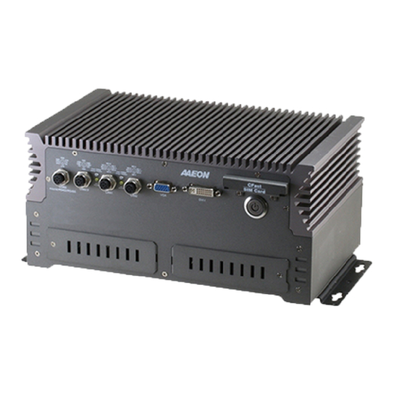
- Page 1 BOXER-6357VS Railway Embedded Box PC User’s Manual 4 Last Updated: April 29, 2016...
- Page 2 Copyright Notice This document is copyrighted, 2016. All rights are reserved. The original manufacturer reserves the right to make improvements to the products described in this manual at any time without notice. No part of this manual may be reproduced, copied, translated, or transmitted in any form or by any means without the prior written permission of the original manufacturer.
- Page 3 Acknowledgement All other products’ name or trademarks are properties of their respective owners. Microsoft Windows is a registered trademark of Microsoft Corp. Intel, Pentium, Celeron, and Xeon are registered trademarks of Intel Corporation Core, Atom are trademarks of Intel Corporation ...
- Page 4 Packing List Before setting up your product, please make sure the following items have been shipped: Item Quantity BOXER-6357VS Wallmount bracket Screw (M2 x 3 mm) Screw (M4 x 6 mm) Drive bay keys Waterproof power kit ...
- Page 5 About this Document This User’s Manual contains all the essential information, such as detailed descriptions and explanations on the product’s hardware and software features (if any), its specifications, dimensions, jumper/connector settings/definitions, and driver installation instructions (if any), to facilitate users in setting up their product. Users may refer to the AAEON.com for the latest version of this document.
- Page 6 Safety Precautions Please read the following safety instructions carefully. It is advised that you keep this manual for future references All cautions and warnings on the device should be noted. All cables and adapters supplied by AAEON are certified and in accordance with the material safety laws and regulations of the country of sale.
- Page 7 As most electronic components are sensitive to static electrical charge, be sure to ground yourself to prevent static charge when installing the internal components. Use a grounding wrist strap and contain all electronic components in any static-shielded containers. If any of the following situations arises, please the contact our service personnel: Damaged power cord or plug Liquid intrusion to the device iii.
- Page 8 FCC Statement This device complies with Part 15 FCC Rules. Operation is subject to the following two conditions: (1) this device may not cause harmful interference, and (2) this device must accept any interference received including interference that may cause undesired operation.
- Page 9 China RoHS Requirements (CN) 产品中有毒有害物质或元素名称及含量 AAEON Embedded Box PC/ Industrial System 有毒有害物质或元素 部件名称 铅 汞 镉 六价铬 多溴联苯 多溴二苯醚 (Pb) (Hg) (Cd) (Cr(VI)) (PBB) (PBDE) 印刷电路板 ○ ○ ○ ○ ○ ○ 及其电子组件 外部信号 ○ ○ ○ ○ ○ ○ 连接器及线材...
- Page 10 China RoHS Requirement (EN) Poisonous or Hazardous Substances or Elements in Products AAEON Embedded Box PC/ Industrial System Poisonous or Hazardous Substances or Elements Hexavalent Polybrominated Polybrominated Component Lead Mercury Cadmium Chromium Biphenyls Diphenyl Ethers (Pb) (Hg) (Cd) (Cr(VI)) (PBB) (PBDE) PCB &...
-
Page 11: Table Of Contents
Table of Contents Chapter 1 - Product Specifications ..................1 Specifications ......................2 Chapter 2 – Hardware Information ..................5 Dimensions ....................... 6 List of Jumpers ......................8 2.2.1 Clear CMOS Selection (JP1) ............9 2.2.2 Dry and Wet Contact Digital Output Power Selection (JP2) ... 9 2.2.3 Dry and Wet Contact Digital Iutput Power Selection (JP3) .. - Page 12 Chapter 3 - AMI BIOS Setup ....................20 System Test and Initialization ................21 AMI BIOS Setup ..................... 22 Setup Submenu: Main ..................23 Setup Submenu: Advanced ................. 24 3.4.2 Advanced: SATA Configuration ........... 25 3.4.3 Advanced: USB Configuration ............. 26 3.4.4 Advanced: Hardware Monitor .............
- Page 13 Memory Address Map ..................62 IRQ Mapping Chart ....................63 DMA Channel Assignments ................76 Appendix C – RAID & AHCI Settings ................... 77 Setting RAID ......................78 Setting AHCI ......................88 Appendix D – Digital I/O Ports .................... 94 DI/O Programming ....................
-
Page 14: Chapter 1 - Product Specifications
Chapter 1 Chapter 1 - Product Specifications... -
Page 15: Specifications
Specifications System ® Intel Core™ i7-3517UE, up to 2.8 GHz Processor DDR3 1333/1600 SODIMM x 2, up to. 16 GB System Memory (4 GB preinstalled) ® Intel QM77 Chipset Display DVI-I x 1 (DVI-A x DVI-D) Interface DB-15 x 1 Storage... - Page 16 Serial Port RS-232/422/485 x 2 (DB-9, non-isolated) RS-232/422/485 x 1 (DB-9, isolated) Display - - Others Isolated digital input x 4 Isolated digital output x 2 Line-out x 1 Mic-in x 1 Power input connector (refer to Power Supply for details) Antenna opening x 3 (for WiFi, GPS, 3G/4G respectively) Expansion...
- Page 17 Mounting Wall-mounted Operating Temperature -40 ~ 70°C (-40 ~ 158°F), 85°C (185°F) for 10 minutes only Storage Temperature -40 ~ 80°C (-40°F ~ 176°F) Dimension (W x H x D) 286 x 135 x 174.2 mm (112.60” x 68.58” x ...
-
Page 18: Chapter 2 - Hardware Information
Chapter 2 Chapter 2 – Hardware Information... -
Page 19: Dimensions
Dimensions Chapter 2 – Hardware Information... - Page 20 ISOLATION COM3 COM2 COM1 ISOLATION RS232/RS422/RS485 RS232/RS422/RS485 USB 3.0/2.0 RS232/RS422/RS485 AUDIO VI DI4 DI3 DI2 DI1 GND +5V DO2 DO1 VOI DC-IN MX+2 MX+2 USB+ USB- MX-2 MX-1 MX-2 MX-1 USB- USB+ MX+3 MX+1 MX+3 MX+1 MX+0 MX-0 MX+0 MX-0 Green-100Mbps Green-100Mbps MX-3...
-
Page 21: List Of Jumpers
List of Jumpers Please refer to the table below for all of the system’s jumpers that you can configure for your application Label Function Clear CMOS Selection Dry and Wet Contact Digital Output Power Selection Dry and Wet Contact Digital Input Power Selection COM2 12V/5V/RI Selection COM3 12V/5V/RI Selection AT/ATX Mode Selection... -
Page 22: Clear Cmos Selection (Jp1)
2.2.1 Clear CMOS Selection (JP1) Normal (Default) Clear CMOS 2.2.2 Dry and Wet Contact Digital Output Power Selection (JP2) Wet contact (3~30V) Dry contact (system 5V) 2.2.3 Dry and Wet Contact Digital Iutput Power Selection (JP3) Wet contact (3~30V) Dry contact (system 5V) 2.2.4 COM2/3 12V/5V/RI (JP4/5) +12V Ring (default) -
Page 23: At/Atx Mode Selection (Jp6)
2.2.5 AT/ATX Mode Selection (JP6) ATX mode AT mode Chapter 2 – Hardware Information... -
Page 24: List Of Connectors
List of Connectors Please refer to the table below for all of the system’s connectors that you can configure for your application Label Function M12 Ethernet 1 M12 Ethernet 2 Front Panel Connector BIOS SPI Flash Header CN18 LPC Connector CN22 USB 3.0 Connector CN23... -
Page 25: M12 Ethernet 1/2 (Cn1/2)
2.3.1 M12 Ethernet 1/2 (CN1/2) Signal Signal MX-0 MX+0 MX+3 MX-2 MX+2 MX-1 MX+1 MX-3 2.3.2 Front Panel Connector (CN6) Signal Signal POWER SWITCH HDLED LED POWER HWRST 2.3.3 BIOS SPI Flash Header (CN7) Signal Signal 3.3 V Chapter 2 – Hardware Information... -
Page 26: Lcp Connector (Cn18)
2.3.4 LCP Connector (CN18) Signal Signal 3.3 V FRAME DRQ0 DRQ1 2.3.5 USB 3.0 Connector (CN22) Signal Signal VBUS SSRX- SSRX+ GND_DRAIN SSTX- SSTX+ SHIELD 2.3.6 USB 2.0 Connector (CN23) Signal Signal Chapter 2 – Hardware Information... -
Page 27: Digital Input/ Output (Cn35)
ENABLE 2.3.7 Digital Input/ Output (CN35) Signal Signal DI_POWER DO_POWER OUTPUT_POWER Dry and Wet Contact Digital Input Chapter 2 – Hardware Information... - Page 28 Dry Contact Wiring Wet Contact Wiring Digital Input Voltage Range 10 ~ 25V Pin Name Signal Type Signal Level DRY (5V) WET Digital input 1 Input (3~30V) DRY (5V) WET Digital input 2 Input (3~30V) DRY (5V) WET Digital input 3 Input (3~30V) Chapter 2 –...
- Page 29 DRY (5V) WET Digital input 4 Input (3~30V) WET contact 3~30V POWER Dry and Wet Contact Digital Output Dry Contact Wiring Wet Contact Wiring Digital Output Voltage Range Pin Name Signal Type Signal Level Digital Output Input 3 ~ 30 V Power Open collector to Digital output 1...
-
Page 30: Com2/3 Rs-232/422/485 Connector (Cn38/39)
2.3.8 COM2/3 RS-232/422/485 Connector (CN38/39) Signal Signal DCD (422TXD-/ RXD (422RXD+) 485DATA+) TXD (422TXD+/ DTR (422RXD-) 485DATA+) 2.3.9 Isolated COM1 RS-232/422/485 Connector (CN40) Signal Signal DCD (422TXD-/ RXD (422RXD+) 485DATA-) TXD (422TXD+/ DTR (422RXD-) 485DATA+) Chapter 2 – Hardware Information... -
Page 31: M12 Usb 2.0 X 2 (Usbm1)
2.3.10 M12 USB 2.0 x 2 (USBM1) Signal Signal USB1- USB1+ USB2- USB2+ 2.3.11 PSON Connector (PSONCN1) Signal Signal PSON# 2.3.12 Power Switch (PWESW1) Signal Signal POWER SWITCH 2.3.13 Power Standby Connector (LEDSB5VCN12) Signal Signal Chapter 2 – Hardware Information... -
Page 32: Power Led Connector (Ledcn19)
LED+/ 5V_DUAL 2.3.14 Power LED Connector (LEDCN19) Signal Signal LED+/ +5VS 2.3.15 MiniCard Slot (Full-MiniCard) (CN17) Signal Signal +5VS HDD_SWAPLED- Chapter 2 – Hardware Information... -
Page 33: Chapter 3 - Ami Bios Setup
Chapter 3 Chapter 3 - AMI BIOS Setup... -
Page 34: System Test And Initialization
System Test and Initialization The system uses certain routines to perform testing and initialization. If an error, fatal or non-fatal, is encountered, a few short beeps or an error message will be outputted. The board can usually continue the boot up sequence with non-fatal errors. The system configuration verification routines check the current system configuration against the values stored in the CMOS memory. -
Page 35: Ami Bios Setup
AMI BIOS Setup The AMI BIOS ROM has a pre-installed Setup program that allows users to modify basic system configurations, which is stored in the battery-backed CMOS RAM and BIOS NVRAM so that the information is retained when the power is turned off. To enter BIOS Setup, press <Del>... -
Page 36: Setup Submenu: Main
Setup Submenu: Main Chapter 3 – AMI BIOS Setup... -
Page 37: Setup Submenu: Advanced
Setup Submenu: Advanced Chapter 3 – AMI BIOS Setup... -
Page 38: Advanced: Sata Configuration
3.4.2 Advanced: SATA Configuration Options summary: Enable Optimal Default, Failsafe Default SATA Controllers Disable En/Disable SATA Controller Optimal Default, Failsafe Default SATA Mode Selection AHCI Determines how SATA controller(s) operate Chapter 3 – AMI BIOS Setup... -
Page 39: Advanced: Usb Configuration
3.4.3 Advanced: USB Configuration Options summary: Legacy USB Support Enable Optimal Default, Failsafe Default Disable Enables Legacy USB support. AUTO option disables legacy support if no USB devices are connected. DISABLE option will keep USB devices available only for EFI applications. Smart Auto Optimal Default, Failsafe Default Auto... -
Page 40: Advanced: Hardware Monitor
3.4.4 Advanced: Hardware Monitor Chapter 3 – AMI BIOS Setup... -
Page 41: Advanced: Dynamic Digital Io Configuration
3.4.5 Advanced: Dynamic Digital IO Configuration Options summary: DIO_P#5 Direction[Output] Output Level Optimal Default, Failsafe Default Set DIO_P#5 output as Hi or Low DIO_P#6 Direction[Output] Output Level Optimal Default, Failsafe Default Set DIO_P#6 output as Hi or Low Chapter 3 – AMI BIOS Setup... -
Page 42: Advanced: Amt Configuration
3.4.6 Advanced: AMT Configuration Options summary: Disabled Intel AMT Enabled Optimal Default, Failsafe Default Enable/Disable Intel (R) Active Management Technology BIOS Extension. Note : iAMT H/W is always enabled. This option controls the BIOS extension execution only. If enabled, additional firmware in the SPI device is required Disabled Optimal Default, Failsafe Default Un-Configure ME... -
Page 43: Advanced: Super Io Configuration
3.4.7 Advanced: Super IO Configuration Chapter 3 – AMI BIOS Setup... -
Page 44: Super Io Configuration: Serial Port 1 Configuration
3.4.7.1 Super IO Configuration: Serial Port 1 Configuration Options summary: Disabled Serial Port Enabled Optimal Default, Failsafe Default Enable or disable serial port (COM) Auto Optimal Default, Failsafe Default IO=3F5h; IRQ=4 IO=3F8h; IRQ=3,4 Change Settings IO=2F8h; IRQ=3,4 IO=3E8h; IRQ=3,4 IO=2E8h; IRQ=3,4 Select an optimal setting for Super IO device RS232 Optimal Default, Failsafe Default... -
Page 45: Super Io Configuration: Serial Port 2 Configuration
3.4.7.2 Super IO Configuration: Serial Port 2 Configuration Options summary: Disabled Serial Port Enabled Optimal Default, Failsafe Default Enable or disable serial port (COM) Auto Optimal Default, Failsafe Default IO=2F8h; IRQ=3 IO=3F8h; IRQ=3,4 Change Settings IO=2F8h; IRQ=3,4 IO=3E8h; IRQ=3,4 IO=2E8h; IRQ=3,4 Select an optimal setting for Super IO device RS232 Optimal Default, Failsafe Default... -
Page 46: Super Io Configuration: Serial Port 3 Configuration
3.4.7.3 Super IO Configuration: Serial Port 3 Configuration Options summary: Disabled Serial Port Enabled Optimal Default, Failsafe Default Enable or disable serial port (COM) Auto Optimal Default, Failsafe Default IO=3F8h; IRQ=5 Change Settings IO=2E8h; IRQ=5 IO=2D0h; IRQ=5 IO=2D8h; IRQ=5 Select an optimal setting for Super IO device RS232 Optimal Default, Failsafe Default Device Type... -
Page 47: Super Io Configuration: Serial Port 4 Configuration
3.4.7.4 Super IO Configuration: Serial Port 4 Configuration Options summary: Disabled Serial Port Enabled Optimal Default, Failsafe Default Enable or disable serial port (COM) Auto Optimal Default, Failsafe Default IO=2E8h; IRQ=5 Change Settings IO=2E8h; IRQ=5 IO=2D0h; IRQ=5 IO=2D8h; IRQ=5 Select an optimal setting for Super IO device RS232 Optimal Default, Failsafe Default Device Type... -
Page 48: Super Io Configuration: Power Saving Function
3.4.7.5 Super IO Configuration: Power Saving Function Options summary: Disabled Optimal Default, Failsafe Default Power Saving Function Enabled Enable to reduce power consumption in system off state When Enabled, only the power button can activate the system. Chapter 3 – AMI BIOS Setup... -
Page 49: Setup Submenu: Chipset
Setup submenu: Chipset Chapter 3 – AMI BIOS Setup... -
Page 50: Chipset: Pch-Io Configuration
3.5.1 Chipset: PCH-IO Configuration Options summary: Power Mode ATX Type Optimal Default, Failsafe Default AT Type Select Power Supply Mode Restore AC power Power Off Loss Power On Optimal Default, Failsafe Default Last State Select AC power state when power is re-applied after a power failure PCH LAN Controller Enabled Optimal Default, Failsafe Default Disabled... - Page 51 Enable/disable Deep S5/\n\nNote :\n When Deep S5 is enabled, Intel® AMT and Wake On PCH LAN functions are not available in system shut down. Mini PCIe Speed Gen1 Optimal Default, Failsafe Default Gen2 Select Mini PCI Express port speed Chapter 3 – AMI BIOS Setup...
-
Page 52: Chipset: System Agent (Sa) Configuration
3.5.2 Chipset: System Agent (SA) Configuration Options summary: VBIOS Default Optimal Default, Failsafe Default Primary IGFX Boot Display CRT2 Chapter 3 – AMI BIOS Setup... -
Page 53: Setup Submenu: Boot
Setup submenu: Boot Options summary: Quiet Boot Disabled Enabled Default Launch I82579LM PXE OpROM Disabled Default Enabled Launch I82574L PXE OpROM Disabled Default Enabled Chapter 3 – AMI BIOS Setup... -
Page 54: Setup Submenu: Security
Setup submenu: Security Change User/Administrator Password You can set a User Password once an Administrator Password. The password will be required during boot up, or when the user enters the Setup utility. Please Note that a User Password does not provide access to many of the features in the Setup utility. Select the password you wish to set, press Enter to open a dialog box to enter your password (you can enter no more than six letters or numbers). -
Page 55: Setup Submenu: Save & Exit
Setup submenu: Save & Exit Chapter 3 – AMI BIOS Setup... -
Page 56: Chapter 4 - Drivers Installation
Chapter 4 Chapter 4 – Drivers Installation... -
Page 57: Product Cd/Dvd
Product CD/DVD The BOXER-6357VS comes with a product DVD that contains all the drivers and utilities you need to setup your product. Insert the DVD and follow the steps in the autorun program to install the drivers. In case the program does not start, follow the sequence below to install the drivers. Step 1 –... - Page 58 Open the Step 4 - AUDIO folder and select your OS Open the .exe file in the folder Follow the instructions Drivers will be installed automatically Step 5 – Install USB 3.0 Driver (Windows 7 only) Open the Step 5 – USB3.0 folder followed by setup.exe Follow the instructions Drivers will be installed automatically Step 6 –...
- Page 59 Open the Step 7 – ME folder Open setup.exe Follow the instructions Drivers will be installed automatically Step 8 – Install Serial Port Driver (Optional) For Windows XP Open the Step 8 – Serial Port Driver (Optional) folder and select the WinXP_32 folder Open patch.bat Follow the instructions...
- Page 60 For Windows 7: Change User Account Control settings to Never notify Chapter 4 – Driver Installation...
- Page 61 Reboot and log in as administrator Run patch.bat as administrator Chapter 4 – Driver Installation...
- Page 62 For Windows 8: Open the Apps Screen, right click on the Command Prompt tile and select Run as Administrator To install the driver (patch.bat), you will first have to locate the file in command prompt. To do that, go to the folder in which the file resides by entering cd (file path) eg: if the file is in a folder named abc in c drive, enter cd c:\abc (screenshot for reference only) You are now at the folder where the file is located.
- Page 63 Reboot after installation completes. To confirm the installation, go to Device Manager, expand the Ports (COM & LPT) tree and double click on any of the COM ports to open its properties. Go to the Driver tab, select Driver Details and click on serial.sys, you should see its provider as Windows (R) Win 7 DDK Provider.
- Page 64 Chapter 4 – Driver Installation...
-
Page 65: Appendix A - Watchdog Timer Programming
Appendix A Appendix A - Watchdog Timer Programming... -
Page 66: Watchdog Timer Initial Program
A.1 Watchdog Timer Initial Program Table 1 : SuperIO relative register table Default Value Note SIO MB PnP Mode Index Register Index 0x2E(Note1) 0x2E or 0x4E SIO MB PnP Mode Data Register Data 0x2F(Note2) 0x2F or 0x4F Table 2 : Watchdog relative register table Register BitNum Value... - Page 67 ************************************************************************************ // SuperIO relative definition (Please reference to Table 1) #define byte SIOIndex //This parameter is represented from Note1 #define byte SIOData //This parameter is represented from Note2 #define void IOWriteByte(byte IOPort, byte Value); #define byte IOReadByte(byte IOPort); // Watch Dog relative definition (Please reference to Table 2) #define byte TimerLDN //This parameter is represented from Note3 #define byte TimerReg //This parameter is represented from Note4 #define byte TimerVal // This parameter is represented from Note24...
- Page 68 ************************************************************************************ VOID Main(){ // Procedure : AaeonWDTConfig // (byte)Timer : Time of WDT timer.(0x00~0xFF) // (boolean)Unit : Select time unit(0: second, 1: minute). AaeonWDTConfig(); // Procedure : AaeonWDTEnable // This procudure will enable the WDT counting. AaeonWDTEnable(); ************************************************************************************ Appendix A – Watchdog Timer Programming...
- Page 69 ************************************************************************************ // Procedure : AaeonWDTEnable VOID AaeonWDTEnable (){ WDTEnableDisable(EnableLDN, EnableReg, EnableBit, 1); // Procedure : AaeonWDTConfig VOID AaeonWDTConfig (){ // Disable WDT counting WDTEnableDisable(EnableLDN, EnableReg, EnableBit, 0); // Clear Watchdog Timeout Status WDTClearTimeoutStatus(); // WDT relative parameter setting WDTParameterSetting(); VOID WDTEnableDisable(byte LDN, byte Register, byte BitNum, byte Value){ SIOBitSet(LDN, Register, BitNum, Value);...
- Page 70 ************************************************************************************ VOID SIOEnterMBPnPMode(){ IOWriteByte(SIOIndex, 0x87); IOWriteByte(SIOIndex, 0x87); VOID SIOExitMBPnPMode(){ IOWriteByte(SIOIndex, 0xAA); VOID SIOSelectLDN(byte LDN){ IOWriteByte(SIOIndex, 0x07); // SIO LDN Register Offset = 0x07 IOWriteByte(SIOData, LDN); VOID SIOBitSet(byte LDN, byte Register, byte BitNum, byte Value){ Byte TmpValue; SIOEnterMBPnPMode(); SIOSelectLDN(byte LDN); IOWriteByte(SIOIndex, Register); TmpValue = IOReadByte(SIOData);...
-
Page 71: Appendix B - I/O Information
Appendix B Appendix B - I/O Information... -
Page 72: I/O Address Map
I/O Address Map Appendix B – I/O Information... - Page 73 Appendix B – I/O Information...
- Page 74 Appendix B – I/O Information...
-
Page 75: Memory Address Map
Memory Address Map Appendix B – I/O Information... -
Page 76: Irq Mapping Chart
IRQ Mapping Chart Appendix B – I/O Information... - Page 77 Appendix B – I/O Information...
- Page 78 Appendix B – I/O Information...
- Page 79 Appendix B – I/O Information...
- Page 80 Appendix B – I/O Information...
- Page 81 Appendix B – I/O Information...
- Page 82 Appendix B – I/O Information...
- Page 83 Appendix B – I/O Information...
- Page 84 Appendix B – I/O Information...
- Page 85 Appendix B – I/O Information...
- Page 86 Appendix B – I/O Information...
- Page 87 Appendix B – I/O Information...
- Page 88 Appendix B – I/O Information...
-
Page 89: Dma Channel Assignments
DMA Channel Assignments Appendix B – I/O Information... -
Page 90: Appendix C - Raid & Ahci Settings
Appendix C Appendix C – RAID & AHCI Settings... -
Page 91: Setting Raid
Setting RAID OS installation to setup RAID Mode Driver CD ->Step 7 - RAID&AHCI” Step 1: Copy the files below from “ to Disk Step 2: Connect the USB Floppy (disk with RAID files) to the board Appendix C – RAID & AHCI Settings... - Page 92 Step 3: The setting procedures “ In BIOS Setup Menu” A: Advanced -> SATA Configuration -> SATA Mode -> RAID Mode Step 4: The setting procedures “In BIOS Setup Menu” B: Advanced -> Launch Storage OpROM -> Enabled Appendix C – RAID & AHCI Settings...
- Page 93 Step 5: The setting procedures “In BIOS Setup Menu” C: Boot -> Boot Option #1 -> DVD-ROM Type Step 6: The setting procedures “In BIOS Setup Menu” D: Save & Exit -> Save Changes and Exit Appendix C – RAID & AHCI Settings...
- Page 94 Step 7: Press Ctrl-I to enter MAIN MENU Step 8: Choose “1.Create RAID Volume” Appendix C – RAID & AHCI Settings...
- Page 95 Step 9: RAID Level -> RAID0(Stripe) Step 10: Choose “Create Volume” Appendix C – RAID & AHCI Settings...
- Page 96 Step 11: Choose “Y” Step 12: Choose “5. Exit” Appendix C – RAID & AHCI Settings...
- Page 97 Step 13: Choose “Y” Step 14: Setup OS Appendix C – RAID & AHCI Settings...
- Page 98 Step 15: Press “F6” Step 16: Choose “S” Appendix C – RAID & AHCI Settings...
- Page 99 Step 17: Choose “Intel(R) Mobile Express Chipset SATA RAID Controller” Step 18: It will show the model number you select and then press “ENTER” Appendix C – RAID & AHCI Settings...
- Page 100 Step 19: Setup is starting Windows Appendix C – RAID & AHCI Settings...
-
Page 101: Setting Ahci
Setting AHCI OS installation to setup AHCI Mode Driver CD ->Step 7 - RAID&AHCI” Step 1: Copy the files below from “ to Disk Step 2: Connect the USB Floppy (disk with AHCI files) to the board Appendix C – RAID & AHCI Settings... - Page 102 Step 3: The setting procedures “ In BIOS Setup Menu” A: Advanced -> SATA Configuration -> SATA Configuration -> SATA Mode -> AHCI Mode Step 4: The setting procedures “In BIOS Setup Menu” B: Boot -> Boot Option #1 -> DVD-ROM Type Appendix C –...
- Page 103 Step 5: The setting procedures “In BIOS Setup Menu” C: Save & Exit -> Save Changes and Exit Step 6: Setup OS Appendix C – RAID & AHCI Settings...
- Page 104 Step 7: Press “F6” Step 8: Choose “S” Appendix C – RAID & AHCI Settings...
- Page 105 Step 9: Choose “Intel(R) 7 Series Chipset Family SATA AHCI Controller” Step 10: It will show the model number you select and then press “ENTER” Appendix C – RAID & AHCI Settings...
- Page 106 Step 11: Setup is loading files Appendix C – RAID & AHCI Settings...
-
Page 107: Appendix D - Digital I/O Ports
Appendix D Appendix D – Digital I/O Ports... -
Page 108: Di/O Programming
DI/O Programming BOXER-6357VS utilizes FINTEK F81866 chipset as its Digital I/O controller. Below are the procedures to complete its configuration. AAEON initial DI/O program is also attached for developing customized program for your application. There are three steps to complete the configuration setup: (1) Enter the MB PnP Mode (2) Modify the data of configuration registers (3) Exit the MB PnP Mode. -
Page 109: Digital I/O Register
Digital I/O Register Table 1 : SuperIO relative register table Default Value Note SIO MB PnP Mode Index Register Index 0x2E(Note1) 0x2E or 0x4E SIO MB PnP Mode Data Register Data 0x2F(Note2) 0x2F or 0x4F Table 2 : Digital Input relative register table Register BitNum Value... -
Page 110: Digital I/O Sample Program
Digital I/O Sample Program ************************************************************************************ // SuperIO relative definition (Please reference to Table 1) #define byte SIOIndex //This parameter is represented from Note1 #define byte SIOData //This parameter is represented from Note2 #define void IOWriteByte(byte IOPort, byte Value); #define byte IOReadByte(byte IOPort); // Digital Input Status relative definition (Please reference to Table 2) #define byte DInput1LDN // This parameter is represented from Note3 #define byte DInput1Reg // This parameter is represented from Note4... - Page 111 ************************************************************************************ // Digital Output control relative definition (Please reference to Table 3) #define byte DOutput1LDN // This parameter is represented from Note27 #define byte DOutput1Reg // This parameter is represented from Note28 #define byte DOutput1Bit // This parameter is represented from Note29 #define byte DOutput1Val // This parameter is represented from Note30 #define byte DOutput2LDN // This parameter is represented from Note31 #define byte DOutput2Reg // This parameter is represented from Note32...
- Page 112 ************************************************************************************ VOID Main(){ Boolean PinStatus ; // Procedure : AaeonReadPinStatus // Input : Example, Read Digital I/O Pin 3 status // Output : InputStatus : 0: Digital I/O Pin level is low 1: Digital I/O Pin level is High PinStatus = AaeonReadPinStatus(DInput3LDN, DInput3Reg, DInput3Bit); // Procedure : AaeonSetOutputLevel // Input : Example, Set Digital I/O Pin 6 level...
- Page 113 ************************************************************************************ Boolean AaeonReadPinStatus(byte LDN, byte Register, byte BitNum){ Boolean PinStatus ; PinStatus = SIOBitRead(LDN, Register, BitNum); Return PinStatus ; VOID AaeonSetOutputLevel(byte LDN, byte Register, byte BitNum, byte Value){ ConfigToOutputMode(LDN, Register, BitNum); SIOBitSet(LDN, Register, BitNum, Value); ************************************************************************************ Appendix D – Digital I/O Ports...
- Page 114 ************************************************************************************ VOID SIOEnterMBPnPMode(){ IOWriteByte(SIOIndex, 0x87); IOWriteByte(SIOIndex, 0x87); VOID SIOExitMBPnPMode(){ IOWriteByte(SIOIndex, 0xAA); VOID SIOSelectLDN(byte LDN){ IOWriteByte(SIOIndex, 0x07); // SIO LDN Register Offset = 0x07 IOWriteByte(SIOData, LDN); VOID SIOBitSet(byte LDN, byte Register, byte BitNum, byte Value){ Byte TmpValue; SIOEnterMBPnPMode(); SIOSelectLDN(byte LDN); IOWriteByte(SIOIndex, Register); TmpValue = IOReadByte(SIOData);...
- Page 115 ************************************************************************************ Boolean SIOBitRead(byte LDN, byte Register, byte BitNum){ Byte TmpValue; SIOEnterMBPnPMode(); SIOSelectLDN(LDN); IOWriteByte(SIOIndex, Register); TmpValue = IOReadByte(SIOData); TmpValue &= (1 << BitNum); SIOExitMBPnPMode(); If(TmpValue == 0) Return 0; Return 1; VOID ConfigToOutputMode(byte LDN, byte Register, byte BitNum){ Byte TmpValue, OutputEnableReg; OutputEnableReg = Register-1;...