Yamaha LoopFactory DX200 Service Manual
Hide thumbs
Also See for LoopFactory DX200:
- Owner's manual (152 pages) ,
- Owner's manual (82 pages) ,
- User manual (9 pages)
Advertisement
Quick Links
This document is printed on chlorine free (ECF) paper with soy ink.
SY 011594
20010301-59800
SERVICE MANUAL
CONTENTS
SPECIFICATIONS .............................................................................. 3
PANEL LAYOUT .................................................................................. 4
CIRCUIT BOARD LAYOUT ................................................................. 6
WIRING ............................................................................................... 6
BLOCK DIAGRAM .............................................................................. 7
DISASSEMBLY PROCEDURE ........................................................... 8
LSI PIN DISCRIPTION ....................................................................... 11
IC BLOCK DIAGRAM ........................................................................ 15
DIMENSIONS ................................................................................... 17
CIRCUIT BOARDS ........................................................................... 18
TEST PROGRAM & INITIALIZE ....................................................... 28
MIDI IMPLEMENTATION CHART ..................................................... 40
PARTS LIST
OVERALL CIRCUIT DIAGRAM
HAMAMATSU, JAPAN
1.494k-377Y.K
Printed in Japan '01, 03
Advertisement

Related Manuals for Yamaha LoopFactory DX200


Summary of Contents for Yamaha LoopFactory DX200
- Page 1 SERVICE MANUAL CONTENTS SPECIFICATIONS ................3 PANEL LAYOUT .................. 4 CIRCUIT BOARD LAYOUT ..............6 WIRING ....................6 BLOCK DIAGRAM ................7 DISASSEMBLY PROCEDURE ............8 LSI PIN DISCRIPTION ............... 11 IC BLOCK DIAGRAM ................ 15 DIMENSIONS ................... 17 CIRCUIT BOARDS ................18 TEST PROGRAM &...
- Page 2 IMPORTANT NOTICE This manual has been provided for the use of authorized Yamaha Retailers and their service personnel. It has been assumed that basic service procedures inherent to the industry, and more specifically Yamaha Products, are already known and understood by the users, and have therefore not been restated.
- Page 3 9.DIMENSIONS,WEIGHT 338.0(W) x 208.9(D) x 51.7(H) mm, 1600 g 10. ACCESSORIES CD ROM (for Windows and Macintosh) Owner's Manual AC Adaptor (Power supply recommendation may vary from country to country. Please check with your nearest Yamaha dealer for further details.)
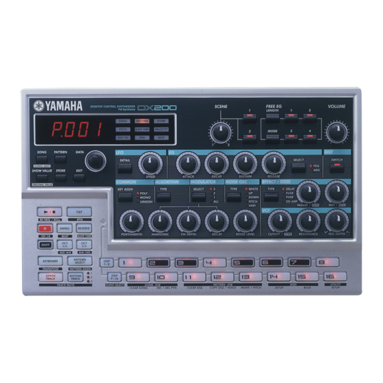
- Page 4 DX200 PANEL LAYOUT Top Panel Main block Voice block Control block Keyboard block Main Block [SONG] [PATTERN] [DATA] knob [SHOW VOLUME] [STORE] [EXIT] VOICE BLOCK [SCENE] group [SCENE] knob [1] button [2] button [FREE EG] group [LENGTH] button [1] button [2] button [MODE] button [3] button...
- Page 5 DX200 [RELEASE] knob [SELECT] button [DIST] group [SWITCH] button [COMMON] group [KEY ASGN] button [ALGORITHM] group [TYPE] button [MODULATOR] group [SELECT] button [NOISE OSC] group [TYPE] button [PORTAMENTO] knob [HARMONIC] knob [FM DEPTH] knob [DECAY] knob [NOISE LEVEL] knob [EFFECT MIXER] group [TYPE] button [PARAM / PAN] knob [WET / VOL] knob...
- Page 6 DX200 CIRCUIT BOARD LAYOUT PLG150-DX WIRING CN2(7P) CN5(15P) CN6(4P) CN4(6P) CN3(15P) CN1(15P) PLG150-DX CN4(6P) CN2(15P) CN3(4P) 28C99-8818208 LOCATION CONNECTOR NAME PIN/LENGTH DESTINATION 16P / L=80 PN-CN1 LED-CN1 7P / L=450 KR-KR PN-CN5 DM-CN2 4P / L=380 DS-KR DM-CN6 PN-CN3 15P / L=220 DS-KR PN-CN2 DM-CN3...
- Page 7 SWING REVERS << >> KEYBOARD PATTERN SELECT STEP STEP TRACK TRACK 9~16...
- Page 8 DX200 DISASSEMBLY PROCEDURE [180] DX200 Bottom side Bottom Assembly Wooden bolster (Fig. 1) (Fig. 1-1) [180]: Bind Head Tapping Screw-B 3.0X6 MFZN2Y (EP600130) Bottom Assembly (time required: about 1 min) Remove the seven (7) screws marked [180]. The bottom assembly can then be removed. (Fig. 1) If you turn the mixer upside down for disaasembling and assembling, put 2 wooden bolsters underneath the unit at its both side ends to...
- Page 9 DX200 DM Circuit Board (time required: about 2 min) Remove the bottom assembly. (See Procedure 1.) Remove the PLG150-DX circuit Board. (See Procedure 2.) Remove the six (6) screws marked [120]. The DM circuit board can then be removed. (Fig. 2) Attachment consideration of the DM circuit board Confirm that the DM contact terminal (110b), which is on the backside of the DM circuit board,...
- Page 10 DX200 [40] (Fig. 5) [40]: Bind Head Tapping Screw-P 2.6X8 MFZN2Y (EP620100) LED Circuit Board (time required: about 5 min) Remove the bottom assembly. (See Procedure 1.) Remove the PLG150-DX circuit Board. (See Procedure 2.) Remove the DM circuit Board. (See Procedure 3.) Remove the PN circuit Board.
- Page 11 DX200 LSI PIN DISCRIPTOIN HG73C205AFD (XU947C00) SWX00B TONE GENERATOR DM: IC17 NAME FUNCTION NAME FUNCTION Initial clear CMA3 RFCLKI PLL Clock CMA8 Program address bus PLL Control CMA2 AVDD_PLL Power supply read signal AVSS_PLL Ground CMA1 Program address bus MODE0 SWX dual mode high byte effective signal VCC7...
- Page 12 DX200 HD6437043E00F (XS936A00) CPU PLG150-DX: IC2 NAME FUNCTION NAME FUNCTION /WRHH HH write DACK0 DMA transfer strobe Data bus /WRHL HL write /CASHH HH Column address strobe PE15 Port E Power supply Ground Data bus Ground Address bus Data bus Power supply Address bus Power supply...
- Page 13 DX200 YMP706-F (XT329A00) FS1-AB AWM Tone Generator & Digital Filter PLG150-DX: IC8 NAME FUNCTION NAME FUNCTION CHIN0 TEST Channel data input CHIN1 TEST CHOUT0 Ground Channel data output CHOUT1 TEST Ground TEST TEST TEST TEST TEST TEST Address input TEST Power supply TEST TEST...
- Page 14 DX200 µ PD63200GS-E1 (XP867A00) DAC (Digital to Analog Converter) DM: IC16 NAME FUNCTION NAME FUNCTION 4/8F 4/8 Fs selection R. REF Channel R voltage reference L. REF Channel L voltage reference D. GND Digital ground L. OUT Channel L output 16 BIT 16 bit/18 bit selection D.
- Page 15 DX200 IC BLOCK DIAGRAM SN74HC157NSR (XW110A00) HD74HC74FPEL (XL096A00) TC9246F -TEL(XR339A00) MM74HC157SJX(XY310A00) Phase Locked Loop TC74HC74AF(EL) (XW890A00) Quad 2 to 1 Multiplexer MM74HC74ASJX (XY153A00) PLG150-DX: IC9 DM: IC7 Dual D-Type Flip-Flop DM: IC14, IC25 Lock SELECT date Phase LOCK defect STROBE Programmable 1CLR VDDA...
- Page 16 DX200 TC74HC14AF NJM3414AM-T1 (XR294A00) TC74HCT04AF-T1 (XI297A00) (XD657A00) MM74HC14JX Dual Operational Amplifier Hex Inverter (XW104A00) Hex Inverter DM: IC4 DM: IC5 PN: IC9 PGL150-DX: IC1 +DC Voltage Output A Supply Inverting Output B Input A Non-Inverting Inverting Input A Input B Non-Inverting -DC Voltage Supply Input B...
- Page 17 DX200 DIMENSIONS 51.7 mm (H) SONG PATTERN STORE PITCH GATE TIME VELOCITY INST SEL BEAT 338 mm (W)
- Page 18 DX200 CIRSUIT BOARD DM CIRCUIT BOARD OUTPUT STAND BY MIDI PHONES DC IN L/MONO to PN CN5 to PLG150-DX CN1 to PN CN3 Battery VN103500 VN103600 (Battery holder for VN103500) Battery DM: 2NA-V625760 2 Notice for back-up battery removal push the battery as shown in figure, then the battery will pop up.
- Page 19 DX200 MIDI to PN CN3 to PN CN4 to PN CN2 to PN CN6 Component side DM: 2NA-V625760 2 Note: See parts list for details of circuit board component parts.
- Page 20 DX200 DM CIRCUIT BOARD DM: 2NA-V625760 2...
- Page 21 DX200 Pattern side DM: 2NA-V625760 2...
- Page 22 DX200 DM CIRCUIT BOARD PN CIRCUIT BOARD to DM CN6 to DM CN3 to DM CN4 LED (LD12~LD14) LED Speacer PN Circuit Board PN: 2NA-V488620 °...
- Page 23 DX200 to DM CN4 Component side PN: 2NA-V488620 Note: See parts list for details of circuit board component parts.
- Page 24 DX200 PN CIRCUIT BOARD PN: 2NA-V488620...
- Page 25 DX200 Pattern side PN: 2NA-V488620 Note: See parts list for details of circuit board component parts.
- Page 26 DX200 PLG150-DX Circut Board to DM CN5 Component side Pattern side Note: See parts list for details of circuit board component parts. PLG150-DX: 2NA-V414740...
- Page 27 DX200 LED CIRCUIT BOARD Component side SONG PATTERN STORE PITCH GATE TIME VELOCITY INST SEL BEAT Note: See parts list for details of circuit board component parts. LED: 2NA-V488650...
- Page 28 DX200 TEST PROGRAM & INITIALIZE 1. TEST PROGRAM PREPERATIONS Following measuring instruments and jigs are required for the test. Measuring instruments : frequency counter(input impedance: more than 1M Ω) oscilloscope(input impedance: more than 1M Ω) volt meter(JIS-C curve, input impedance: more than 1M Ω, 0 dBm: 1mW 600 Ω) distortion meter(input impedance: more than 1M Ω) digital multimeter(input impedance: more than 1M Ω) keyboard amplifier(a KS15-equivalence)
- Page 29 DX200 The test program Test No. Test Item Test Conditions, Judgment Criteria, etc OK/NG RAM BATTERY OK/NG SW & LED OK/NG LED visually check the lights DATA ENTRY OK/NG (0-23-0) KNOB OK/NG (255,254-127-1, 0) MIDI OK/NG WAVE ROM OK/NG 1kHz OUTPUT(L) +3.0 +/- 2dBm load 10kΩ...
- Page 30 DX200 C-3 SW & LED Display of Test Results Press the panel switches according to the order indicated by the LCD and confirm that all switches are working properly. Confirm that the LED corresponding to the panel switch lights on. After about one second, LED display and all LED’s light on for about Test End three seconds and then off to indicate following on the display:...
- Page 31 DX200 -4.0 +/- 2 dBm (load 33 Ω) ADistortion: less than C-6 MIDI PHONES-L: 0.6% less than -60dBm(load 33 Ω) PHONES-R: Display of Test Results Not appearing After connecting the MIDI IN to the MIDI OUT via a MIDI cable, Test End execute the test.
- Page 32 DX200 C-11 PB RAM Frequency: 1kHz +/- 3Hz Level: -2.0dBm +/- 2dBm Display of Test Results Not appearing Test End Check RAM of the plug-in board which is built in the unit. Rotate [DATA ENTRY] knob clockwise to proceed to the next test. Display of Test Results C-14 FACTORY SET This test is used to initialize the data to the factory settings.
- Page 33 This appears when the voltage of the internal backup battery becomes Err1 Err1 Err1 Err1 Err1 Battery Low low. Have the battery replaced by your local Yamaha dealer or any (flashes) Yamaha-authorized service personnel. This appears when too much MIDI data has been received at one time, Err2 Err2 Err2...
- Page 34 DX200...
- Page 35 DX200...
- Page 36 DX200...
- Page 37 DX200...
- Page 38 DX200...
- Page 39 DX200...
- Page 40 DX200 MIDI IMPLEMENTATION CHART YAMAHA [ DESKTOP CONTROL SYNTHESIZER ] Date:23-JAN-2001 Model DX200 MIDI Implementation Chart Version : 1.0 Transmitted Recognized Remarks Function... Basic Default 1 - 16 1 - 16 Memorised Channel Changed 1 - 16 1 - 16...
- Page 41 DX200 PARTS LIST CONTENTS OVERALL ASSEMBLY .................. 2 PN ASSEMBLY ..................... 4 ELECTRICAL PARTS ................... 5 Note) DESTINATION ABBREVIATIONS Australian model South African model British model Chinese model Canadian model South-east Asia model German model Taiwan model European model U.S.A. model French model General export model (110V) North European model...
- Page 42 DX200 OVERALL ASSEMBLY Upper Case Assembly PN Assembly See page 4. Bottom Assembly 170b 170a...
- Page 43 DX200 DESCRIPTION REMARKS PART NO. QTY RANK REF NO. Overall Assembly DX200 JUEW (V678980) V 6 9 5 3 2 0 0 Upper Case Assembly Upper Case NA0643 (V679190) V 6 5 5 3 6 0 0 Protector V 7 5 4 3 7 0 0 Adhesive Tape #500 8mm V 6 5 5 4 2 0 0...
- Page 44 DX200 PN ASSEMBLY PART NO. DESCRIPTION REMARKS QTY RANK REF NO. DX200 PN ASSEMBLY (V679230) PN Assembly V 5 8 3 0 7 0 0 Circuit Board V 4 1 6 2 6 0 0 LENGHT, MODE, LFO DETAIL, Button EG SELECT, KEY ASGN, ALGORITHM TYPE, MODULATOR SELECT,...
- Page 45 DX200 ELECTRICAL PARTS DESCRIPTION REMARKS PART NO. QTY RANK REF NO. ELECTRICAL PARTS DX200 V 4 8 8 6 1 0 0 DM J Circuit Board (XZ156D0) V 4 8 8 6 4 0 0 Circuit Board LED J (XZ192D0) V 5 8 3 0 7 0 0 circuit Board PN J...
- Page 46 DX200 DESCRIPTION REMARKS PART NO. QTY RANK REF NO. UF038100 Electrolytic Cap. (chip) 100 16V US061220 22P 50V J Ceramic Capacitor-CH(chip) US061270 27P 50V J Ceramic Capacitor-CH(chip) US063100 1000P 50V K Ceramic Capacitor-B (chip) US063220 Ceramic Capacitor-B (chip) 2200P 50V K US135100 Ceramic Capacitor-F (chip) 0.1000 16V Z...
- Page 47 DX200 DESCRIPTION REMARKS PART NO. QTY RANK REF NO. X I 2 9 7 A 0 0 TC74HCT04AF-T1 INVERTER XW104A00 INVERTER MM74HC14SJX XP263A00 OP AMP M5216FP-600C XQ138A00 OP AMP NJM4556AMT1 XW110A00 SN74HC157NSR MALTIPLEXER XY310A00 MM74HC157SJX MALTIPLEXER XR682A00 TC7S66F BILATERAL SWITCH X I 6 8 6 A 0 0 IC10 M62021FP...
- Page 48 DX200 DESCRIPTION REMARKS PART NO. QTY RANK REF NO. RD356470 Carbon Resistor (chip) 4.7K 63M J RD356470 Carbon Resistor (chip) 4.7K 63M J RD355220 Carbon Resistor (chip) 220 63M J RD355220 Carbon Resistor (chip) 220 63M J RD355220 Carbon Resistor (chip) 220 63M J RD356470 Carbon Resistor (chip)
- Page 49 DX200 DESCRIPTION REMARKS PART NO. QTY RANK REF NO. RD357220 Carbon Resistor (chip) 22K 63M J RD354560 Carbon Resistor (chip) 56 63M J RD354560 Carbon Resistor (chip) 56 63M J RD354560 Carbon Resistor (chip) 56 63M J RD357220 Carbon Resistor (chip) 22K 63M J RD357220 Carbon Resistor (chip)
- Page 50 DX200 DESCRIPTION REMARKS PART NO. QTY RANK REF NO. XU533A00 HD74HC273FP D-FF XY198A00 MM74HC273SJX D-FF XU533A00 HD74HC273FP D-FF XY198A00 MM74HC273SJX D-FF XS720A00 TC74HC245AF TRANSCEIVER XV611A00 HD74HC245FPV TRANSCEIVER XW107A00 MM74HC245ASJX TRANSCEIVER XU533A00 HD74HC273FP D-FF XY198A00 MM74HC273SJX D-FF XU533A00 HD74HC273FP D-FF XY198A00 MM74HC273SJX D-FF XU533A00...
- Page 51 DX200 DESCRIPTION REMARKS PART NO. QTY RANK REF NO. V 3 9 9 0 4 0 0 LD57 TLOU1008 V 6 4 8 7 0 0 0 LN282RPX-(TX3) RED LD58 V 6 4 8 7 0 0 0 LD59 LN282RPX-(TX3) RED VU067800 LD60 SEL6210S-TP5 RED...
- Page 52 DX200 DESCRIPTION REMARKS PART NO. QTY RANK REF NO. UB051150 Monolithic Ceramic Cap. SL 15P 50V J UB445470 F 0.470 16V Z Monolithic Ceramic Cap. UB044100 F 0.010 50V Z Monolithic Ceramic Cap. UB245100 F 0.100 25V Z Monolithic Ceramic Cap. VY722900 Tantalum Capacitor 10 10V M...
- Page 53 <P. 1> DX200 DX200 OVERALL CIRCUIT DIAGRAM (DM) to PN CN2 to PN CN4 to PN CN5 OP AMP PHONES OUTPUT L / MONO REGURATOR +5V OUTPUR R TRANSCEIVER MULTIPLEXER OP AMP OP AMP OP AMP INVERTER INVERTER INVERTER REGURATOR +3.3V D-FF µPC2909T(XT441A00) SI-8050S(LF1103)
- Page 54 <P. 2> DX200 DX200 OVERALL CIRCUIT DIAGRAM (PN, LED) to DM CN3 to DM CN4 to DM CN4 28CCI-8818207 to DM CN2 D-FF D-FF MULTIPLEXER TRANSCEIVER D-FF MULTIPLEXER OP AMP D-FF 28CCI-8818206 D-FF Note: See parts list for details of circuit board component parts. DX200 DX200...
- Page 55 PLG150-DX FRASH ROM 4M FRASH ROM 4M DRAM 4M GATE ARRAY MDSP D-FF INVERTER 28CA1-8812205...