Table of Contents
Advertisement
SERVICE MANUAL
COLOR TELEVISION/
DVD VIDEO PLAYER
This supplement serves as an update to the original Service Manual, file number 140-200228.
Please refer to this Supplement in conjunction with the original Service Manual when servicing
this model.
MD9DM1R comes with 2 versions of CHROMA IC. The version can be identified by the
alphabet behind the serial no. (Eg. 49E62001 B).
When replacing components use only those in the respective list (version A or B). IC605 and C605
must be changed together following the Electrical Replacement Parts list if the original parts are not
available. Versions A and B are interchangeable by combination parts change.
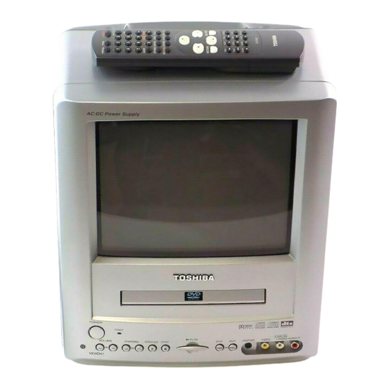
MD9DM1R
SUMMARY
MFR'S VERSION
A
B
FILE NO. 140-200246
SUPPLEMENT
IC601
TB1253N
TB1253AN
DOCUMENT CREATED IN JAPAN, Oct., 2002
Advertisement
Table of Contents

Related Manuals for Toshiba MD9DM1R


Summary of Contents for Toshiba MD9DM1R
- Page 1 Please refer to this Supplement in conjunction with the original Service Manual when servicing this model. MD9DM1R comes with 2 versions of CHROMA IC. The version can be identified by the alphabet behind the serial no. (Eg. 49E62001 B). When replacing components use only those in the respective list (version A or B). IC605 and C605 must be changed together following the Electrical Replacement Parts list if the original parts are not available.
- Page 2 ELECTRICAL ADJUSTMENTS (VERSION B) 2-17: Confirmation of Fixed Value (Step No.) Please check if the fixed values of the each adjustment items are set correctly referring below. FUNCTION STEP NO FUNCTION STEP NO BRIGHTNESS(MAX) BRI. AV(MAX) BRIGHTNESS(MIN) BRI. AV(MIN) COLOR(MAX) COL.
- Page 3 TOSHIBA VIDEO PRODUCTS PTE. LTD. 438B ALEXANDRA ROAD, BLOCK B #06-01 ALEXANDRA TECHNOPARK SINGAPORE 119968...
- Page 4 FILE NO. 140-200228 SERVICE MANUAL COLOR TELEVISION/ DVD VIDEO PLAYER MD9DM1R...
-
Page 5: Caution
CAUTION THIS DIGITAL VIDEO PLAYER EMPLOYS A LASER SYSTEM. TO ENSURE PROPER USE OF THIS PRODUCT, PLEASE READ THIS SERVICE MANUAL CARE- FULLY AND RETAIN FOR FUTURE REFERENCE. SHOULD THE UNIT REQUIRE MAINTENANCE, CONTACT AN AUTHORIZED SERVICE LOCATION-SEE SERVICE PROCEDURE. USE OF CONTROLS, ADJUSTMENTS OR THE PERFORMANCE OF PROCEDURES OTHER THAN THOSE SPECIFIED HEREIN MAY RESULT IN HAZARDOUS RADIATION EXPOSURE. -
Page 6: Important Safeguards
IMPORTANT SAFEGUARDS READ INSTRUCTIONS All the safety and operating instructions should be read before the unit is operated. RETAIN INSTRUCTIONS The safety and operating instructions should be retained for future reference. HEED WARNINGS All warnings on the unit and in the operating instructions should be adhered to. FOLLOW INSTRUCTIONS All operating and use instructions should be followed. - Page 7 IMPORTANT SAFEGUARDS (CONTINUED) DAMAGE REQUIRING SERVICE Unplug this unit from the wall outlet and refer servicing to qualified service personnel under the following conditions: When the power-supply cord or plug is damaged. If liquid has been spilled, or objects have fallen into the unit. If the unit has been exposed to rain or water.
-
Page 8: Disc Removal Method At No Power Supply
DISC REMOVAL METHOD AT NO POWER SUPPLY Remove the Back Cabinet and Power PCB/DVD Block. (Refer to item 1 of the DISASSEMBLY INSTRUCTIONS.) Rotate the black gear of Deck CD section in the direction of the arrow by hand, remove the disc from Deck CD. -
Page 9: Table Of Contents
TABLE OF CONTENTS CAUTION ..........................A1-1 IMPORTANT SAFEGUARDS ....................A1-2, A1-3 DISC REMOVAL METHOD AT NO POWER SUPPLY ............A1-4 PARENTAL CONTROL - RATING LEVEL ................A1-4 TABLE OF CONTENTS ......................A2-1 GENERAL SPECIFICATIONS ....................A3-1~A3-6 DISASSEMBLY INSTRUCTIONS 1.REMOVAL OF MECHANICAL PARTS AND P.C. BOARDS ..........B1-1, B1-2 2.REMOVAL OF ANODE CAP .................... -
Page 10: General Specifications
GENERAL SPECIFICATIONS CRT Size / Visual Size 9 inch / 228.6 mmV System CRT Type Normal Deflection 90 degree Magnetic Field BV/BH +0.45G / 0.18G Color System NTSC Speaker 2 Speaker Position Side Size 3 inch Impedance 8 ohm Sound Output 1.2W + 1.2W 10%(Typical) 0.8W + 0.8W... - Page 11 GENERAL SPECIFICATIONS Power Power Source 120V, 60Hz Power Consumption at AC at 120V 60Hz at DC at 12V Stand by (at AC) at 120V 60Hz Per Year -- kWh/Year Protector Power Fuse Regulation Safety Radiation X-Radiation DHHS Laser DHHS Temperature Operation +5oC ~ +40oC Storage...
- Page 12 GENERAL SPECIFICATIONS G-10 On Screen Menu (DVD) Display Menu Type Character Language Menu SubTitle Audio Picture TV Screen Size OSD Display On/Off Sound DRC (Dynamic Range Control) dts Decode Output(5.1ch/ 2ch) Surround On/Off Center On/Off Sub Woofer On/Off Parental Password Lock/ Un Lock Rating Level Other OSD Language(Set up Language)
- Page 13 GENERAL SPECIFICATIONS G-12 Remote Unit RC-EF Control Glow in Dark Remocon Format Custom Code 71-8E h Power Source Voltage(D.C) UM size x pcs UM-4 x 2 pcs Total Keys 45 Key Keys Power Play Stop Search+ Search- Skip+ Skip- Slow+ Slow- Pause Call...
- Page 14 (Dolby Digtal) (DTS) Surround (Spatializer N-2-2) Screen Saver G-14 Accessories Owner's Manual Language English w/Guarantee Card Buyer Model No MD9DM1R Remote Control Unit Battery UM size x pcs UM-4 x 2 pcs OEM Brand Rod Antenna Poles Terminal Loop Antenna Terminal...
- Page 15 GENERAL SPECIFICATIONS G-15 Interface Switch Front Power (Tact) Channel Up Channel Down Volume Up Volume Down Play Open/Close Skip(>>) Skip(<<) Still/Pause Stop Main Power SW Rear Main Power SW Indicator Power Stand-by On Timer Terminals Front Video Input RCA x 1 Audio Input RCA x 2(Stereo) Other Terminal...
-
Page 16: Disassembly Instructions
DISASSEMBLY INSTRUCTIONS 1. REMOVAL OF MECHANICAL PARTS 1-3: TV/DVD BLOCK (Refer to Fig. 1-3) Remove the 2 screws 1. AND P.C. BOARDS Disconnect the following connectors: 1-1: BACK CABINET (Refer to Fig. 1-1) (CP301, CP302, CP401 and CP403). Remove the 4 screws 1. Remove the TV/DVD Block in the direction of arrow. - Page 17 DISASSEMBLY INSTRUCTIONS 1-5: FRONT TRAY PLATE/TOP SHIELD Pick Up PCB (Refer to Fig. 1-5) Unlock the 2 supports 1. Remove the Front Tray Plate in the direction of arrow (A). Remove the 13 screws 2. Remove the Top Shield in the direction of arrow (B). CD Deck Make the sort circuit Top Shield...
-
Page 18: Removal Of Anode Cap
DISASSEMBLY INSTRUCTIONS 2. REMOVAL OF ANODE CAP 3. After one side is removed, pull in the opposite direction to remove the other. Read the following NOTED items before starting work. NOTE After turning the power off there might still be a potential Take care not to damage the Rubber Cap. -
Page 19: Removal Of Deflection Yoke
DISASSEMBLY INSTRUCTIONS 4. Insert one end of the Anode Support into the anode button, then the other as shown in Fig. 2-5. Support Fig. 2-5 Confirm that the Support is securely connected. Put on the Rubber Cap without moving any parts. 3. -
Page 20: Removal And Installation Of Flat Package Ic
DISASSEMBLY INSTRUCTIONS REMOVAL AND INSTALLATION OF When IC starts moving back and forth easily after desoldering completely, pickup the corner of the IC using FLAT PACKAGE IC a tweezers and remove the IC by moving with the IC desoldering machine. (Refer to Fig. 4-3.) REMOVAL NOTE Put the Masking Tape (cotton tape) around the Flat... - Page 21 DISASSEMBLY INSTRUCTIONS INSTALLATION When bridge-soldering between terminals and/or the soldering amount are not enough, resolder using a Thin- Take care of the polarity of new IC and then install the tip Soldering Iron. (Refer to Fig. 4-8.) new IC fitting on the printed circuit pattern. Then solder each lead on the diagonal positions of IC temporarily.
-
Page 22: Service Mode List
SERVICE MODE LIST This unit provided with the following SERVICE MODES so you can repair, examine and adjust easily. To enter to the SERVICE MODE function, press and hold both buttons simultaneously on the main unit and on the remote control for more than a standard time (second). -
Page 23: Servising Fixturws And Tools
WHEN REPLACING EEPROM (MEMORY) IC If a service repair is undertaken where it has been required to change the MEMORY IC, the following steps should be taken to ensure correct data settings while making reference to TABLE 1. Note: No need setting for the position of the mark @ due to the adjustment value. Table 1 Enter DATA SET mode by setting VOLUME to minimum. -
Page 24: Electrical Adjustments
ELECTRICAL ADJUSTMENTS BEFORE MAKING ELECTRICAL FUNCTION FUNCTION ADJUSTMENTS R CUT OFF BRI. AV(CENT.) G CUT OFF BRI. AV(MAX) Read and perform these adjustments when repairing the B CUT OFF BRI. AV(MIN) G DRIVE COL. AV(CENT.) circuits or replacing electrical parts or PCB assemblies. B DRIVE COL. - Page 25 ELECTRICAL ADJUSTMENTS 2-4: WHITE BALANCE 2-9: VERTICAL LINEARITY NOTE: Adjust after performing CUT OFF adjustment. NOTE: Adjust after performing adjustments in section 2-8. After the adjustment of Vertical Linearity, reconfirm Place the set with Aging Test for more than 15 minutes. the Vertical Position and Vertical Size adjustments.
- Page 26 ELECTRICAL ADJUSTMENTS 2-12: SEPARATION 2-13: SUB BRIGHT CENTER Please do the method (1) or method (2) adjustment. Receive the monoscope pattern. (RF Input) Using the remote control, set the brightness and Method (1) contrast to normal position. Set the multi-sound signal generator for each different Activate the adjustment mode display of Fig.
- Page 27 ELECTRICAL ADJUSTMENTS 2-14: SUB TINT CENTER 2-15: SUB COLOR CENTER Receive the color bar pattern. (RF Input) Receive the color bar pattern. (RF Input) Using the remote control, set the brightness, contrast, Using the remote control, set the brightness, contrast, color and tint to normal position.
-
Page 28: Power
ELECTRICAL ADJUSTMENTS 2-16: SUB CONTRAST MAX Activate the adjustment mode display of Fig. 1-1 and press the channel button (15) on the remote control to select "CNTX". Press the RIGHT/LEFT button on the remote control until the contrast step No. becomes "31" Receive a broadcast and check if the picture is normal. - Page 29 ELECTRICAL ADJUSTMENTS PURITY AND CONVERGENCE 3-3: STATIC CONVERGENCE ADJUSTMENTS NOTE Adjust after performing adjustments in section 3-2. NOTE Receive the crosshatch pattern from the color bar Turn the unit on and let it warm up for at least 30 generator. minutes before performing the following adjustments.
- Page 30 ELECTRICAL ADJUSTMENTS 4. ELECTRICAL ADJUSTMENT PARTS LOCATION GUIDE (WIRING CONNECTION) CD850 CD803 CP850B CD801 CRT PCB CP801 J801 CD820 CP8001 CP850A CP820A MAIN PCB J503 CP810B CP301 CP302 CP811 FB401 CP8002 VR501 VR502 SPEAKER SPEAKER CD401 CP401 TOP SHIELD R449 CD8002 TP401 CP402...
- Page 31 MECHANICAL EXPLODED VIEW PCB110 (CRT PCB ASS'Y) PCB070 (MAIN PCB ASS'Y)
- Page 32 MECHANICAL EXPLODED VIEW PCB130 (DVD PCB ASS'Y) PCB250 (AV PCB ASS'Y)
- Page 33 MECHANICAL REPLACEMENT PARTS LIST Location No. TSB P/N Reference No. Description BZ310495 A5C101I720 CABINET,FRONT ASSY BZ710467 753WSA0133 SHIELD,TV MAIN PCB BZ710786 761WPAA064 COVER,FBT BZ710459 761WPA0223 HOLDER,FBT BZ710039 8995034000 CORD CLIP UL CO. BZ710697 761WPA0250 HOLDER,FFC BZ710698 761WSA0093 ANGLE,DECK BZ710787 752WSA0299 PLATE,BOTTOM BZ710401 769WPA0018...
- Page 34 ELECTRICAL REPLACEMENT PARTS LIST Location No. TSB P/N Reference No. Description RESISTORS ! R404 BZ210112 R4X5T6152F R,METAL 1.5K OHM 1/6W ! R439 BZ210089 R4X5T6273F R,METAL 27K OHM 1/6W ! R440 BZ210090 R4X5T6822F R,METAL 8.2K OHM 1/6W ! R441 BZ210091 R4X5T6104F R,METAL 100K OHM 1/6W ! R442...
- Page 35 ELECTRICAL REPLACEMENT PARTS LIST Location No. TSB P/N Reference No. Description DIODES ! D411 BZ410014 D2LTPG06J0 DIODE,SILICON RMPG06J-G3 ! D412 BZ410014 D2LTPG06J0 DIODE,SILICON RMPG06J-G3 ! D413 BZ410014 D2LTPG06J0 DIODE,SILICON RMPG06J-G3 ! D415 BZ410063 D2WTAU02A0 DIODE,SILICON AU02A-EIC D416 BZ410090 D97U04R71B DIODE,ZENER MTZJ4.7B T-77 D501 BZ410061...
- Page 36 ELECTRICAL REPLACEMENT PARTS LIST Location No. TSB P/N Reference No. Description IC902 BZ611068 I01FF58290 AN5829S IC1001 BZ611123 ICQF067050 ZR36705 IC1006 BZ611124 I5HJ004BF0 S-24C04BFJ-TB IC2001 BZ611125 I53F086610 LC78661W IC2002 BZ611106 I59J0258B3 MSM5416258B-30 IC2301 BZ611126 I03F065600 LA6560 IC2601 BZ611127 I07F04066F BU4066BCF IC2602 BZ611128 I03FR97020 LA9702WL...
- Page 37 ELECTRICAL REPLACEMENT PARTS LIST Location No. TSB P/N Reference No. Description TRANSISTORS Q2606 BZ510109 TCAA3875SY TRANSISTOR,SILICON KTC3875S_Y_RTK Q2607 BZ510113 T27T030180 2SK3018 Q2608 BZ510109 TCAA3875SY TRANSISTOR,SILICON KTC3875S_Y_RTK Q2609 BZ510109 TCAA3875SY TRANSISTOR,SILICON KTC3875S_Y_RTK Q2610 BZ510109 TCAA3875SY TRANSISTOR,SILICON KTC3875S_Y_RTK Q2611 BZ510108 TAAA1504SY TRANSISTOR,SILICON KTA1504S_Y_RTK Q2612 BZ510113...
- Page 38 ELECTRICAL REPLACEMENT PARTS LIST Location No. TSB P/N Reference No. Description JACKS J4202 BZ614399 060J411018 RCA JACK MSP-213V1-432 PBSN J4204 BZ614280 060G421020 RCA JACK HTJ-032-05AR J4205 BZ614147 060G421017 RCA JACK HTJ-032-05AW J4206 BZ614146 060G421016 RCA JACK HTJ-032-05AY SWITCHES SW101 BZ612010 0504101T34 SWITCH,TACT EVQ21505R...
- Page 39 ELECTRICAL REPLACEMENT PARTS LIST Location No. TSB P/N Reference No. Description MISCELLANEOUS CD2302 BZ614436 06CU251002 CORD,CONNECTOR CU251002 CD2601 BZ614437 122H0O2102 CORD,JUMPER 2H0O2102 CD8002 BZ614438 122H0I0102 CORD,JUMPER 2H0I0102 CD8501 BZ614414 06CU2D3001 CORD,CONNECTOR CU2D3001 CD8502 BZ614503 06CU263701 CORD,CONNECTOR CU263701 CP2301 BZ614439 069EV83020 CONNECTOR PCB SIDE 00_6232_008_102_800 CP2302...
- Page 40 DVD FRONT/BACK END BLOCK DIAGRAM TV BLOCK FRONT BACK DRAM SDRAM 1.9V REG IC2002 Y(DVD_Y) IC4002 IC4006 4SM5416258B-30 MSM56V16160F-8 PQ070XZ01ZP MA/MD_ C, H, D MA/MD_ CD/DVD MD/MA_DATA DATA DATA C(DVD_C) A, B, C, D, E, F MECHA T+/– RFN/P X4001 F+/–...
- Page 41 TV BLOCK DIAGRAM TU001 SCL SDA AGC IF SAW FILTER CF203 Q205 PRE AMP FROM DVD BLOCK C(DVD_C) CHROMA/IF Y(DVD_Y) IC601 TB1253N MEMORY IC199 RESET AT+5V S-24C08ADPA-01 IC103 R.OUT PST3245NR AT+5V G.OUT V801 Q4209,Q4211 B.OUT MIXER Q4212,Q4210 AUDIO_L(DVD_A_L) IC4201 VOL DOWN AUDIO_L(DVD_A_R) MUTE SW NJM4580M...
- Page 42 POWER BLOCK DIAGRAM SOUND+B AT+8V +5V REG. IC3001 KIA7805API Q3005 P.CON+8V P.CON+D5V DRIVER AT+5V +5V REG. F501 D501 P.CON+A5V TRANSFORMER IC3002 KIA7805API SWITCHING RECTIFIER AC IN T501 TV POWER H SW REG. Q505 Q507 IC501 STR-G6623 Q504, Q508 LTV-817-VB FEED BACK PROTECTOR FEED BACK CONTROL...
-
Page 43: Printed Circuit Boards
PRINTED CIRCUIT BOARDS DVD (BOTTOM SIDE) DVD (TOP SIDE) CP2301 C2301 CP2302 B2601 Q2302 Q2303 CP2601 B2606 R2307 R2324 C1018 R2302 Q2301 Q2304 L1001 Q2612 Q2603 Q2604 R2671 C4041 B4004 C2658 Q2615 C2620 C2602_1 C2612 Q2613 Q2616 C2023 C2050 R2607 IC4006 C2611 R2606... - Page 44 PRINTED CIRCUIT BOARDS AV (INSERTED PARTS) SOLDER SIDE OS101 CP301 IC3003 W147 IC301 W002 R3018 D3001 HS301 R3009 W834 IC3002 W053 W176 W052 SW110 W808 W051 C3021 W802 W050 R102 R301 W001 W049 SW109 W046 R106 W188 R4238 R123 W820 W114 W187 W012...
- Page 45 PRINTED CIRCUIT BOARDS AV (CHIP MOUNTED PARTS) SOLDER SIDE Q4216 C351 R913 R4281 R203 Q202 Q204 R222 IC902 R208 R210 R215 C617 Q4218 Q203 R606 C628 C224 C929 R212 R226 R619 R220 Q4214 C204 Q601 C4237 C4249 Q602 R605 R218 Q205 R213 R625...
- Page 46 PRINTED CIRCUIT BOARDS MAIN/CRT (INSERTED PARTS) SOLDER SIDE CP820B D403 C527 CP810B D505 CP803A W826 W043 D545 L503 D412 RY503 W046 W828 IC503 W019 T502 W823 D552 W045 D550 D524 FB401_1 W028 R549 D532 W818 W026 R535 Q516 VR501 W024 W061 W023 C432...
- Page 47 PRINTED CIRCUIT BOARDS MAIN/CRT (CHIP MOUNTED PARTS) SOLDER SIDE C805 R814 C810 C811 C809 R812 R813 R811 Q401 R424 R429 C409 Q408 Q504 Q507 C516 R508 Q515 R509 Q404 C506 Q407 Q518 R531 C531 R540 Q506 Q522 C541 Q513 C545 R521 Q514 R527...
-
Page 48: Mpeg
MPEG SCHEMATIC DIAGRAM (DVD PCB) C4039 W818 0.1 F C4037 0.1 F R4012 W829 4.7K FROM/TO DSP MPEG_AT+3.3V MPEG_+1.9V DVDSTB TP4007 DVDSOS 27MHZ C4012 DVDERR 2.0 2.0 1.9 2.2 2.1 1.9 1.9 1.9 2.8 1.61 2.8 3.27 3.27 0 1.2 0 1.89 1.62 3.24 1.02 0 1.0 3.24 3.24 0 1.63 3.24... - Page 49 MEMORY SCHEMATIC DIAGRAM (DVD PCB) FLASH IC4005 SST39VF800A-70-4C-EK S-DRAM IC4002 MSM56V16160F-8 HA17 HA16 FROM/TO SYSCON1 R4030 HA15 FLASHCS MD15 I/O15 I/O0 HWRH HA14 MD14 I/O14 I/O1 HD10 HD15 HA13 HD11 DQ15 HD12 VSSQ VSSQ HD13 HA12 HD14 HD15 MD13 I/O13 I/O2 HD14 HA11...
- Page 50 FROM/TO TV POWER SYSCON1 SCHEMATIC DIAGRAM CD8502 (CP811) (DVD PCB) CU263701 P.CON+D5V P.CON+5V L1001 P.CON+A5V P.CON+5V A 2.2uH 0305 P.CON+9V P.CON+9V A EEPROM GND[M] MOTOR GND IC1006 S-24C04BFJ-TB FROM/TO REGULATOR B1001 CD8501 (CP8001) C1012_1 CU2D3001 TEST FCM2012H-102T04 R1004 B1002 AT+3.3V_M C1016 4.7K R1021...
-
Page 51: Dsp
DSP SCHEMATIC DIAGRAM (DVD PCB) FROM/TO SYSCON1 GND[A] DRAM B2003 IC2002 P.CON+D5V MSM5416258B-30 FCM2012H-102T04 P.CON+A5V AT+3.3V W842 HA12 HA11 HA10 C2002 0.1 B P.CON+A5V DVDRST DVDCS DVDIRQ FROM/TO MOTOR DRIVE NC NC NC NC TP2001 RFPI JVRVO TESTIO JVAIN C2043 R2035 SPD_FG DVDD2... - Page 52 MOTOR DRIVE SCHEMATIC DIAGRAM (DVD PCB) FROM/TO READ CNANNEL P.CON+9V CLOSE OPEN R2314 MOTOR DRIVE IC2301 LA6560 C2309 S-GND R2318 VCONT C2310 DMUTE VCC2 MUTE R2313 VLD- VIN4 FROM/TO SYSCON1 R2317 VLD+ VIN4- 5.6K P.CON+9V VD4+ VIN4+ AT+3.3V VD4- VREF-IN SPD_FG VD3+ VIN1-SW...
- Page 53 READ CHANNEL SCHEMATIC DIAGRAM (DVD PCB) TP2602 B2602 FCM2012H-102T04 DVD LOADER GND[A] DK4001 C2626 DVD-KDR717SK 68P CH C2627 R2630 FROM/TO LOADER Q2606 CDX2_CTL R2604 B2604 KTC3875S_Y_RTK CDX2 R2623 220P CH CD2601 FCM2012H-102T04 R2605 2H0O2102 CDX4_CTL R2634 CDX4 Q2601 R2620 C2616 KTC3875S_Y_RTK R2640 C2634...
- Page 54 AUDIO/VIDEO SCHEMATIC DIAGRAM (DVD PCB) FROM/TO SYSCON1 W833 VCC+9V W802 GND[A] AT+D5V L8505 SPDIF 9.2 8.5 15uH 0305 CPU_RESET REG. VCC+9V Q8506 SYS_MUTE HN1C03F_B CD/DVD AT+3.3V W830 R8516 680 DAC/D[CVBS] CVBS CVBS DAC_A R8515 DAC/C[C] 75 +-1% C(CVBS) FROM/TO MPEG SPDIF-DVD CVBS CVBS CVBS...
- Page 55 REGULATOR SCHEMATIC DIAGRAM FBT+8V DRIVER (AV PCB) Q3006 R3012 KTA1273_Y AT+8V DRIVER Q3005 KTC3209_Y FROM/TO TV POWER P.ON SW Q3007 CP810A (CP810B) KRC102SRTK FROM/TO SOUND AMP B2013H02-12P AT+8V SOUND GND SOUND_GND SOUND+B SOUND+B AT+6V X-RAY TEST FBT+8V P.CON+12V +9V REG +5V REG +5V REG FROM/TO STEREO...
- Page 56 MICON/TUNER SCHEMATIC DIAGRAM TEST POINT TU001 TECC1040PG32E CP101 07JQ-ST (AV PCB) I2C SCL I2C SDA I2C_OFF I2C OFF R174 TUNER_AGC AUDIO_OUT_L 100 1/4W AUDIO OUIT L AUDIO_OUT_R AUDIO OUT R AT+30V TUNER_AGC FROM/TO I/O CHROMA+5V AUDIO_OUT_L AUDIO_OUT_R TUNER_IF TV/DVD C118 EXT_MUTE R140 FROM/TO AV SW...
- Page 57 VIF/SIF/CHROMA SCHEMATIC DIAGRAM (AV PCB) L601 L203 100uH 0305 100uH 0305 EXT AUDIO DRV. Q204 KTC3875S_Y_RTK R220 R226 T.V.BUF. FROM/TO REGURATOR Q203 KTC3875S_Y_RTK P.CON+A5V L209 56uH CLAMP V.OUT L201 R208 Q202 W826 KTC3875S_Y_RTK R202 18uH H.OUT 3.3K W861 CF201 DVD_C EFCT4R5MW5 DVD_Y CHROMA+5V...
- Page 58 SOUND AMP SCHEMATIC DIAGRAM (AV PCB) HS301 763WAA0117 L CH CP301 SP301 SPEAKER TID-X02P-M1 SA08A05BWC SP OUT L+ 8 OHM SP OUT L- R CH CP302 SPEAKER TID-X02P-M1 SP OUT R+ 8 OHM FROM/TO REGURATOR SP OUT R- SP302 SOUND+B SA08A05BWC C301 R342...
- Page 59 IN/OUT SCHEMATIC DIAGRAM (AV PCB) MUTE SW Q4205 KRA102SRTK MUTE SW Q4207 FROM/TO AV SW KTC3875S_Y_RTK R4225 MONITOR_AUDIO_L MUTE SW MUTE SW Q4204 2.2K Q4208 MONITOR_AUDIO_R KTC3875S_Y_RTK KTC3875S_Y_RTK R4214 R4226 DVD_A_L 10K 1/4W 2.2K DVD_A_R SWD_V_OUT L4202 R4209 R4266 R4270 100uH 9A06B D AUDIO DRIVER R4205...
- Page 60 AV SW SCHEMATIC DIAGRAM (AV PCB) R4217 FRONT AUDIO(R) J4204 HTJ-032-05AR 1/2W C4256 R4281 BUFFER Q4216 KTC3875S_Y_RTK J4205 HTJ-032-05AW FRONT AUDIO(L) C4264 R4282 BUFFER Q4218 KTC3875S_Y_RTK J4206 HTJ-032-05AY FROM/TO I/O FRONT VIDEO MONITOR_AUDIO_L MONITOR_AUDIO_R DVD_A_L DVD_A_R SWD_V_OUT FROM/TO REGURATOR L4205 P.CON+9V 100uH 0305 DVD_VIDEO...
- Page 61 STEREO SCHEMATIC DIAGRAM (AV PCB) FROM/TO MICON/TUNER R911 100 1/4W R912 100 1/4W FROM/TO AV SW TUNER_A_L TUNER_A_R FROM/TO VIF/SIF/CHROMA TU_AUDIO NC 0 OUT SW IIC Decoder St.PLL Pilot Input Switch L-R Filter L-R Demod Cancel Matrix De-Emph (L-R)/SAP Pilot Filter Filter Filter...
- Page 62 DC JACK J503 HEC0824-010010 CAUTION: DIGITAL TRANSISTOR TV POWER SCHEMATIC DIAGRAM RY503 ALKS325 D550 MTZJ6.2B (MAIN PCB) D502 DC POWER SW 1SS133 Q501 PROTECTOR NOTE: THE RESISTOR MARKED F IS FUSE RESISTOR. KTC3198 Q518 THE ALUMI ELECTROLYTIC CAPACITOR MARKED NP 10.9 KRC102SRTK DC POWER SW.
- Page 63 DEFLECTION SCHEMATIC DIAGRAM (MAIN PCB) CP403 A1561WV2-2P V.OUTPUT IC401 LA78040 W888 THERMAL PROTECTION PUMP UP DEGAUSE SW Q401 26.3 12.5 25.9 KRA102SRTK C419 W884 500V FROM/TO DY CP401 B04B-DVS TO CRT CD801_1 C404 SM1098-009-1A 0.0022 B R413_1 R426 R416 R421 5.6K 1/4W 12K +-1% 68K 1/4W...
- Page 64 CRT SCHEMATIC DIAGRAM (CRT PCB) 132.9 104.1 132.8 132.5 TP801 R802 J801 FROM VIF/SIF/CHROMA HPS3200-010501 15K 1W CP850B (CP850A) RED AMP 52147-0510 Q804 B.OUT 2SC3468 102.1 R807 R.OUT 2.7K 1/2W G.OUT CLAMP R811 C809 560P CH TP802 R805 15K 1W GREEN AMP Q805 2SC3468...
- Page 65 COMMAND TRANSMITTER TM101 INTERCONNECTION DIAGRAM HEADPHONE JACK J301 TO OS101 OS101 PIC-37143SY FRONT VIDEO FRONT AUDIO(L) FRONT AUDIO(R) J4206 J4205 J4204 TO SHILED CHASSIS GND CP101 I2C SCL DVD PCB I2C SDA PCB130 I2C OFF VMB261 BLADE AUDIO OUIT L WIDE CD503 CP2601...
-
Page 66: Read Channel
WAVEFORMS MPEG SYSCON TV POWER 10µs 10ns 20ns 5.0V 1.0V 500mV 17.66V 5µs 100ns 20ns 1.00V 1.0V 1.0V 3.44V DEFLECTION 100ns 20ns 0.50V 1.0V 1.0V 5.587V READ CHANNEL 20µs 200mV 200ns 869mV 1.0V 200mV MEMORY 200ns 10.0V 200mV 1.0V 59.0V NOTE: The following waveforms were measured at the point of the corresponding balloon number in the schematic diagram. -
Page 67: Micon/Tuner
WAVEFORMS 50ns 20µs 1.00V 20.0V 200mV 4.57V 0.2µs 20µs 1.00V 100mV 20.0V 5.03V 3.339V 20µs 20µs 20µs 1.00V 1.00V 20.0V 5.19V MICON/TUNER VIF/SIF/CHROMA 0.2ms 20µs 20µs 2.00V 0.50V 1.00V 5.88V 50µs 20ms 20µs 2.00V 1.00V 1.00V 5.54V NOTE: The following waveforms were measured at the point of the corresponding balloon number in the schematic diagram. -
Page 68: Sound Amp
WAVEFORMS IN/OUT 20ms 0.50V 1.00V 2.00V 5.547V STEREO 50µs 200mV 1.00V 2.00V 849mV 10µs 20µs 2.00V 1.00V 1.00V 10.64V SOUND AMP AV SW 20µs 1.00V 0.50V 1.00V 0.50V 1.00V NOTE: The following waveforms were measured at the point of the corresponding balloon number in the schematic diagram. - Page 69 TOSHIBA VIDEO PRODUCTS PTE. LTD. 438B ALEXANDRA ROAD, BLOCK B #06-01 ALEXANDRA TECHNOPARK SINGAPORE 119968...