
Related Manuals for Sony WRT-807B


Summary of Contents for Sony WRT-807B
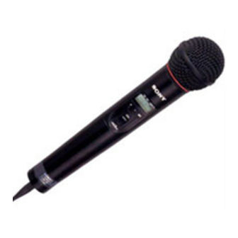
- Page 1 UHF SYNTHESIZED WIRELESS MICROPHONE WRT-807B SERVICE MANUAL U Model CE Model 1st Edition (Revised 3)
- Page 2 électrique, d’incendie ou de blessure n’effectuer que les réparations indiquées dans le mode d’emploi à moins d’être qualifié pour en effectuer d’autres. Pour toute réparation faire appel à une personne compétente uniquement. WRT-807B (U/CE)
-
Page 3: Table Of Contents
4. Spare Parts 4-1. Notes on Repair Parts .................. 4-1 4-2. Exploded View and Parts List ..............4-2 4-3. Electrical Parts List ..................4-4 4-4. Supplied Accessories ................4-16 5. Semiconductor Pin Assignments ..........5-1 6. Block Diagram ..................6-1 WRT-807B (U/CE) - Page 4 7. Board Layouts and Schematic Diagrams 7-1. Board Layouts ..................... 7-1 CN-1868 ....................7-1 DP-306 ...................... 7-1 MB-860 ..................... 7-1 7-2. Schematic Diagrams ..................7-4 CN-1868 ....................7-4 MB-860 ..................... 7-4 DP-306 ...................... 7-8 WRT-807B (U/CE)
-
Page 5: Operating Instructions
Section 1 Reprinted from the Operating Instructions operating instructions WRT-807B (U/CE) - Page 6 WRT-807B (U/CE)
- Page 7 WRT-807B (U/CE)
- Page 8 WRT-807B (U/CE)
- Page 9 WRT-807B (U/CE)
- Page 10 WRT-807B (U/CE)
-
Page 11: Service Overview
B. Don't touch here when removing. Ring Grip B * Tool required . Stop ring removal tool (Sony part No. : J-6402-510-A) DM unit assembly Sub harness (MIC) page Tweezers Sub harness (MIC) Do not press the connector of the DM unit. - Page 12 Antenna Hex. set-screw (2 x 4) Antenna O ring, P15 Tool required . Hex. head screwdriver (Sony part No. : 7-700-766-01) Switch cover, Switch assembly, Grip A Antenna Switch cover Switch assembly Grip A Grip A Ring Switch LRT type...
- Page 13 CN-1868 board WRT-807A (CE, AU) Unsolder. Sub harness (MIC) MB-860 board MB-860 board Chassis A DP-306 board Chassis A Remove the board from the claws. Remove the DP-306 board in the order of 1, 2, 3 and 4. WRT-807B (U/CE)
-
Page 14: Note On Parts Replacement And Reassembly
Chassis A When attaching the DP-306 board to the chassis A, insert the DP-306 board in the order of 1 and 2 in the direction of the arrow as shown, and attach the DP-306 board inside the 2 claws. WRT-807B (U/CE) -
Page 15: Note On Parts Replacement
Confirm that “U42B” (for U42 model) is indicated on the heated tip is applied for too long, so be careful. the display. Confirm that “U62B” (for U62 model) is indicated on the display. Confirm that “U66B” (for U66 model) is indicated on the display. WRT-807B (U/CE) -
Page 17: Electrical Alignment
How to make a AF input cable Required parts 1 pin (black) 2 pin (white) AF input connector ;1 (Part No. J-6402-470-A) Solder. Cable with BNC connector ; 1 (Part No.1-555-758-00) Shield 3 pin (orange) Cable with BNC connector AF input connector (female) WRT-807B (U/CE) -
Page 18: Adjustments
Preparation 1. Remove the MB-860 board, DP-306 board and CN- This section describes the following adjustments and checks 1868 board from WRT-807B unit, and then the MB- required to satisfy specifications. 860, DP-306 and CN-1868 boards must be connected electrically as shown below. -
Page 19: Power Supply Voltage Check
Specification : DC voltage at L101 terminal = +5.0 ± 0.1 Vdc CT200 Frequency counter S101 (POWER) RV301 DP-306 board RV303 RV304 RV302 L101 L102 R366 C376 C369 CT301 CN305 RV305 MB-860 board (B side) MB-860 board (A side) MB-860 board (B side) WRT-807B (U/CE) -
Page 20: Carrier Frequency Adjustment
850.000 MHz ± 1 kHz CE67 model 578.125 MHz ± 1 kHz U30 model 650.125 MHz ± 1 kHz U42 model 770.125 MHz ± 1 kHz U62 model 794.125 MHz ± 1 kHz U66 model Adjustment : 1CT200/DP-306 Board (A side) WRT-807B (U/CE) -
Page 21: Reference Frequency Deviation Adjustment
: 1RV302/MB-860 board (B side) Adjustment Audio analyzer Oscillator (6) After the adjustment has been completed, perform the “3-2-5. Maximum Frequency Deviation Adjustment”. Level meter Switch and Control Setting Same as “Switch and Control Initial Setting” on page 3-3. WRT-807B (U/CE) - Page 22 (CN305) with SMA-BNC (J) connector (and RF conversion connector). Set the modulation analyzer as below; MEASUREMENT : FM MEASUREMENT RANGE : AUTO or ± 100 kHz (manual operation) : 50 Hz : 15 kHz or 20 kHz : 50 us DE EMPHASIS WRT-807B (U/CE)
-
Page 23: Distortion Ratio Check
% (for CE57/CE62/CE67 model)/1.0 % (for U30/U42/ Oscillator U62/U66 model). Level meter SMA-BNC (J) connector with RF conversion connector AF input cable CN-1868 board CN305 MB-860 board (B side) CN303 Switch and Control Setting Same as “Switch and Control Initial Setting” on page 3-3. WRT-807B (U/CE) -
Page 24: S/N Check
(oscillator). cable from audio analyzer (oscillator). (4) Set the audio analyzer to S/N measurement (with A- weighted filter) . (5) Check that the S/N reading is more than 32dB. (with AF input connector (CN303/CN-1868 board) short-circuit- ed). WRT-807B (U/CE) -
Page 25: Tone Signal Adjustment
SMA-BNC (J) connector (Part No. J-6402-490-A) 29 ±1 dB RF conversion connector (Part No. J-6402-400-A) Switch and Control Setting Same as “Switch and Control Initial Setting” on page 3-3. V : 10 dB/div H : 20 kHz/div 32.768 kHz WRT-807B (U/CE) -
Page 26: Battery Alarm Signal Check
: >20 kHz DE EMPHASIS : OFF (3) Check that the frequency counter (resolution : 0.1 Hz CN305 setting) reading is 32.768 kHz ± 1Hz. MB-860 board (B side) SMA-BNC (J) Spectrum connector with analyzer RF conversion connector 3-10 WRT-807B (U/CE) - Page 27 (4) Check that frequency counter (resolution: 0.1 Hz) read- H : 20 kHz/div ing is 32.782 kHz ± 1 Hz. (5) After the checking, remove (unsolder) the jumper wire 32.782 kHz between TONE terminal (land) and GND on the MB- 860 board (B-side). 3-11 WRT-807B (U/CE)
-
Page 28: Spurious Emissions Check
10 dBm MB-860 board (B side) _ 40 dBm connector CN305 Switch and Control Setting V : 10 dB/div Same as “Switch and Control Initial Setting” on page 3-3. H : 500 MHz/div 5 GHz 2.5 GHz (fc) 3-12 WRT-807B (U/CE) -
Page 29: Spare Parts
Therefore, specified parts should be used in the case of replacement. 2. Standardization of Parts Some repair parts supplied by Sony differ from those used for the unit. These are because of parts common- ality and improvement. Parts list has the present standardized repair parts. -
Page 30: Exploded View And Parts List
A-1221-707-A s MOUNTED CIRCUIT BOARD, CN-1868 (Board No. Suffix -31)(U30/U42 model) X-3605-548-1 s SWITCH ASSY X-3678-174-3 s CAGE ASS’Y 1-754-073-12 s ANTENNA (CE57/CE62/U30/U42/U62/U66 model) 1-754-074-12 s ANTENNA (CE67 model) 2-540-969-03 s SCREW (M2X4), LRT 2-545-511-01 o CUSHION, RUBBER 3-603-342-03 o P15,O RING WRT-807B (U/CE) - Page 31 HARNESS (MIC) WRT-807B (U/CE)
-
Page 32: Electrical Parts List
1-691-513-21 s CONNECTOR, BOARD TO BOARD 12P CN303 1-778-965-21 s CONNECTOR 12P CT200 1-141-322-11 s CAPACITOR,VAR,TRIMMER D200 8-719-421-69 s DIODE MA133 D201 8-719-064-05 s DIODE TLGU1002(TPX1,SONY) D202 8-719-421-69 s DIODE MA133 IC200 6-800-709-01 s IC UPD75P3036GK-T807B IC201 8-759-466-70 s IC S-80827ANNP-EDQ-T2 IC202 8-759-277-62 s IC AT93C46-10SI-2.7 (E2) - Page 33 1-216-821-11 s RESISTOR,CHIP 1.0K 1/10W(1608) R202 1-216-821-11 s RESISTOR,CHIP 1.0K 1/10W(1608) R203 1-216-845-11 s RESISTOR,CHIP 100K 1/10W(1608) R204 1-216-833-11 s RESISTOR,CHIP 10K 1/10W (1608) R205 1-216-833-11 s RESISTOR,CHIP 10K 1/10W (1608) 1-216-864-11 s CONDUCTOR, CHIP 0 (1608) (CE57 model) WRT-807B (U/CE)
- Page 34 1-216-821-91 s RES, CHIP 1.0K (1608) R209 1-216-809-91 s RES, CHIP 100 (1608) R210 1-216-857-91 s RES, CHIP 1.0M (1608) R211 1-216-825-91 s RES, CHIP 2.2K (1608) R212 1-216-841-91 s RES, CHIP 47K (1608) R213 1-216-816-91 s RES, CHIP 390 (1608) WRT-807B (U/CE)
- Page 35 1-125-839-11 s CAPACITOR,TANTALUM 47MF/6.3V C320 1-162-965-11 s CAPACITOR,CERAMIC 1500PF/50V B C321 1-104-851-11 s CAPACITOR,TANTALUM 10MF/10V C322 1-162-970-11 s CAPACITOR CERAMIC 0.01MF/25V B C323 1-162-970-11 s CAPACITOR CERAMIC 0.01MF/25V B C324 1-162-927-11 s CAPACITOR,CERAMIC 100PF/50V CH C325 1-164-315-11 s CAPACITOR,CERAMIC 470PF/50V CH WRT-807B (U/CE)
- Page 36 1-162-964-11 s CAPACITOR,CERAMIC 1000PF/50V B L303 1-469-418-11 s INDUCTOR, CHIP 3.3MH C382 1-162-908-11 s CAPACITOR,CERAMIC 3PF/50V 1608 (CE67 model) L304 1-414-470-31 s INDUCTOR, CHIP (J) 39NH 1-162-909-11 s CAPACITOR,CERAMIC 4PF/50V CH L305 1-410-658-31 s INDUCTOR,CHIP 220UH (3225) (CE57/CE62/U62/U66 model) WRT-807B (U/CE)
- Page 37 1-216-845-11 s RESISTOR,CHIP 100K 1/16W(1608) R359 1-216-847-11 s RESISTOR, CHIP 150K 1/16W 1608 R301 1-219-570-11 s RESISTOR,CHIP 10M 1/16W R360 1-216-833-11 s RESISTOR,CHIP 10K 1/16W (1608) R302 1-216-853-11 s RESISTOR,CHIP 470K 1/16W(1608) R361 1-216-845-11 s RESISTOR,CHIP 100K 1/16W(1608) WRT-807B (U/CE)
- Page 38 1-162-970-11 s CAPACITOR CERAMIC 0.01MF/25V B C323 1-162-970-11 s CAPACITOR CERAMIC 0.01MF/25V B C324 1-162-927-11 s CAPACITOR,CERAMIC 100PF/50V CH C325 1-164-315-11 s CAPACITOR,CERAMIC 470PF/50V CH C326 1-164-677-11 s CAPACITOR,CERAMIC 0.033MF/16V C327 1-104-915-11 s CAPACITOR,CHIP 2.2MF/20V C328 1-104-915-11 s CAPACITOR,CHIP 2.2MF/20V 4-10 WRT-807B (U/CE)
- Page 39 1-115-416-11 s CAPACITOR,CERAMIC 1000PF/25V L305 1-410-658-31 s INDUCTOR,CHIP 220UH (3225) L306 1-410-658-31 s INDUCTOR,CHIP 220UH (3225) C386 1-165-176-11 s CAPACITOR,CERAMIC 47000PF/16V L307 1-414-462-11 s INDUCTOR, CHIP (J) 8.2NH (CE62/CE67/U66 model) 1-414-463-41 s INDUCTOR, CHIP (J) 10NH (CE57/U62 model) 4-11 WRT-807B (U/CE)
- Page 40 1-216-809-11 s RESISTOR,CHIP 100 1/10W 1608 R301 1-219-570-11 s RESISTOR,CHIP 10M 1/16W R359 1-218-899-11 s RESISTOR,CHIP 150K 1/10W(1608) R360 1-216-833-11 s RESISTOR,CHIP 10K 1/10W (1608) R302 1-216-853-11 s RESISTOR,CHIP 470K 1/16W(1608) R361 1-216-845-11 s RESISTOR,CHIP 100K 1/10W(1608) 4-12 WRT-807B (U/CE)
- Page 41 1-164-315-91 s CAP, CERAMIC 470PF CH (1608) C327 1-135-179-91 s CAP,CHIP TANTALUM ELECT 2.2MF C328 1-135-179-91 s CAP,CHIP TANTALUM ELECT 2.2MF C330 1-165-176-91 s CAP,CERAMIC 47000PF B 1608 C331 1-104-851-91 s CAP, CHIP TANTALUM ELECT 10MF C332 1-164-230-91 s CAP,CERAMIC 220PF CH 1608 4-13 WRT-807B (U/CE)
- Page 42 8-729-928-91 s TRANSISTOR DTC114EE-TL CN301 1-691-533-21 s CONNECTOR, BOARD TO BOARD 12P Q105 8-729-013-19 s TRANSISTOR 2SC4738-YGR-TE85L CN304 1-779-197-21 s CONNECTOR, BOARD TO BOARD 30P CN305 1-764-243-21 o CONNECTOR (COAXIAL) Q106 8-729-013-19 s TRANSISTOR 2SC4738-YGR-TE85L Q107 8-729-041-51 s TRANSISTOR FMMT617TA 4-14 WRT-807B (U/CE)
- Page 43 1-216-829-91 s RES, CHIP 4.7K (1608) R311 1-216-827-91 s RES, CHIP 3.3K (1608) R372 1-216-825-91 s RES, CHIP 2.2K (1608) R373 1-216-841-91 s RES, CHIP 47K (1608) R312 1-216-826-91 s RES, CHIP 2.7K (1608) R374 1-216-821-91 s RES, CHIP 1.0K (1608) 4-15 WRT-807B (U/CE)
-
Page 44: Supplied Accessories
1-227-410-21 s RES, ADJ, CERMET 10K S101 1-771-756-11 s SWITCH, SLIDE T101 1-475-285-21 s TRANSFORMER, DC-DC CONVERTER T102 1-475-284-21 s TRANSFORMER, DC-DC CONVERTER X301 1-767-314-21 s VIBRATOR, CRYSTAL (0 MHz) X302 1-760-458-21 s VIBRATOR, CRYSTAL (0.032768 MHz) 4-16 WRT-807B (U/CE) - Page 45 Pin assignments and block diagrams are based on the IC manufacturer’s data book. DIODE Page Page TRANSISTOR Page Page 1SS367-T3SONY ..... 5-2 TLGU1002(TPX1,SONY) ... 5-2 2SA1965-TL ..... 5-2 AT93C46-10SI-2.7-E2 ..5-3 2SC4738-YGR-TE85L ..5-2 MA133 ......5-2 2SC4919 ......5-2 CXA1786N-T4 ....5-3 MA133-TX ......5-2 2SC4919-TL ..... 5-2 2SC5015-T1 .....
- Page 46 —TOP VIEW— —TOP VIEW— 1SS367-T3SONY TLGU1002(TPX1,SONY) 2SA1965-TL XN4504 XN4504-TW —TOP VIEW— —TOP VIEW— MA133 2SC4738-YGR-TE85L (MATSUSHITA) 2SC4919 MA133-TX 2SC4919-TL 2SD2216-Q (TOSHIBA) FMMT617TA —TOP VIEW— —TOP VIEW— UMZ8.2T 2SC5015-T1 UMZ8.2T-T106 WIDE —TOP VIEW— DTA144EE DTA144EE-TL —TOP VIEW— DTC114EE (R1=10k,R2=10k) DTC114EE-TL WRT-807B (U/CE)
- Page 47 : OUTPUT FOR DIVIDING SIGNAL OF LxSW PWM CONTROLE COUNTER ERROR AMP. ØR CHIP ENABLE PHASE COMPARATOR ØP PROGRAMMABLE OSCI COUNTER OSCO TEST CHARGE CHARGE PUMP 1 PUMP 2 S-80827ANNP-EDQ-T2 (SEIKO) PULSE SWALLOW VOLTAGE DETECTOR PROGRAMMABLE COUNTER —TOP VIEW— DATA SHIFT RESISTOR LATCH WRT-807B (U/CE)
- Page 48 TC74VHCU04FT(EL) (TOSHIBA) TC4S11F (TOSHIBA) TC4S11F(TE85R) C-MOS HEX INVERTERS —TOP VIEW— C-MOS 2-INPUT NAND GATE —TOP VIEW— GND 3 Y = A • B = 0 : LOW LEVEL 1 : HIGH LEVEL : LOW LEVEL : HIGH LEVEL WRT-807B (U/CE)
- Page 49 4 MHz clock Channel switch _ RESET Reset SET switch — VSS (Ground) EEPROM/PLL Clock EEPROM/PLL data out TONE-OFF Tone off EEPROM chip select 76 to 78 — — PLL latch Transmitted data POFF–OUT Power off — — WRT-807B (U/CE)
-
Page 51: Block Diagram
Block Diagram Description RF circuit block The oscillation circuit utilizes the PLL frequency WRT-807B is comprised of the following : synthesizer method. The VCO (CP301) acts as an MB-860 board oscillator and modulator for the carrier frequency through Power supply circuit block ;... - Page 52 WRT-807B (U/CE)
- Page 53 SUFFIX: -11 SUFFIX: -11 to CN200, DP-306 BOARD SUFFIX: -11, -12 DM UNIT MB-860 CN-1868 -A SIDE- -B SIDE- SUFFIX: -12 SUFFIX: -11 ANTENNA MB-860 CN-1868 -B SIDE- -A SIDE- SUFFIX: -12 SUFFIX: -11 MINUS TERMINAL PLUS TERMINAL WRT-807B (U/CE)
- Page 54 -A SIDE- -B SIDE- SUFFIX: -21 SUFFIX: -21 to CN200, DP-306 BOARD DM UNIT MB-860 CN-1868 -A SIDE- -B SIDE- SUFFIX: -21 SUFFIX: -21 ANTENNA MB-860 CN-1868 -B SIDE- -A SIDE- SUFFIX: -21 SUFFIX: -21 MINUS TERMINAL PLUS TERMINAL WRT-807B (U/CE)
- Page 55 -A SIDE- -B SIDE- SUFFIX: -31 SUFFIX: -31 to CN200, DP-306 BOARD DM UNIT MB-860 CN-1868 -A SIDE- -B SIDE- SUFFIX: -31 SUFFIX: -31 ANTENNA MB-860 CN-1868 -B SIDE- -A SIDE- SUFFIX: -31 SUFFIX: -31 MINUS TERMINAL PLUS TERMINAL WRT-807B (U/CE)
- Page 56 Reference input signal is _55 dB (0 dB = 1 Vrms) and fed with -49.0 -49.0 AF oscillator from MIC connector. For measuring points (A to J), see schematic diagram. -55.0 -55.0 Level values are referential values measured with AF level meter. WRT-807B (U/CE)
- Page 57 DC valtage are taken with digital multimeter (input impedance 1 MZ or more) under no-signal conditions. Voltage values on signal input conditions are taken when the signal is _55 dB (0 dB = 1 Vrms) and fed with AF oscillator from MIC input terminal. WRT-807B (U/CE)
- Page 58 2.2k DTC114EE-TL 1/10W C111 1/10W 0.01uF 1/10W 0.17V C118 Q101 47uF C108 R108 Q107 C117 C107 22uF C109 6.3V FMMT617TA R110 100uF 4.7uF 1/10W FMMT617TA 100uF 1/10W D103 CL102 D104 Q106 Q114 1SS367-T3SONY UMZ8.2T-T106 2SC4738-YGR-TE85L 2SC4738-YGR-TE85L Q113 2SC4738-YGR-TE85L WRT-807B (U/CE)
- Page 59 BOARD NO. 1-674-236-21, 31 C119 4.7uF C121 AF oscillator from MIC connector. 0.1uF WRT-807SM_MB-860_001 For measuring points (A to J), see schematic diagram. Level values are referential values measured with AF level CN-1868 meter. BUSc BOARD NO. 1-674-235-21, 31 WRT-807B (U/CE)
- Page 60 1/16W R211 R213 2.2k 1/16W X200 S200 S201 S202 C203 C219 C201 100uF 0.1uF 47uF D201 6.3V 6.3V TLGU1002(TPX1,SONY) 4MHz C212 C213 C215 C217 C205 C209 CT200 0.1uF 0.1uF 0.1uF 68pF 20pF DP-306 BOARD NO. 1-674-237-11 BUS3 WRT-807-J-M_DP-306_001 WRT-807B (U/CE)
- Page 61 R211 R213 2.2k X200 1/10W 4MHz S200 S201 S202 C219 C201 C203 100uF 0.1uF 47uF 6.3V 6.3V CT200 D201 C212 C213 C215 C217 SML-310MTT86 C205 C209 0.1uF 0.1uF 0.1uF 20pF 68pF DP-306 BOARD NO. 1-674-237-21, 31 WRT-807SM_DP-306_001 BUS3 WRT-807B (U/CE)
- Page 64 Printed in Japan WRT-807B (U, CE) E 2007. 3 08 Sony Corporation 9-976-900-04 ©2001...