Table of Contents
Advertisement
Quick Links
Advertisement
Table of Contents

Related Manuals for Sony IPELA SNC-CS11


Summary of Contents for Sony IPELA SNC-CS11
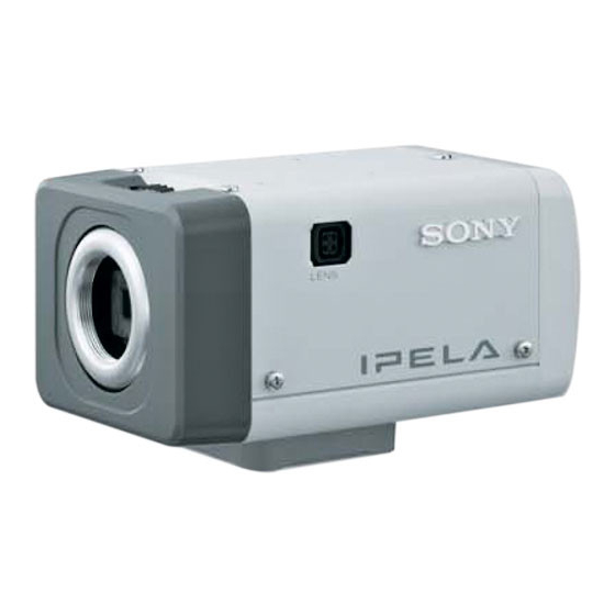
- Page 1 NETWORK CAMERA SNC-CS11 SNC-CS10 SERVICE MANUAL 1st Edition...
- Page 2 ! WARNING This manual is intended for qualified service personnel only. To reduce the risk of electric shock, fire or injury, do not perform any servicing other than that contained in the operating instructions unless you are qualified to do so. Refer all servicing to qualified service personnel.
-
Page 3: Table Of Contents
Table of Contents Manual Structure 3. Circuit Description Purpose of this manual ..............3 3-1. Processing Block of Video and Audio Data ....3-1 3-1-1. Processing Block of Video Data ......3-1 Related manuals ................3 3-1-2. Processing Block of Audio Data ......3-1 Trademarks ................... -
Page 5: Manual Structure
Manual Structure Purpose of this manual This manual is the Service Manual of the Network Camera SNC-CS10/CS11. This manual contains the service overview, adjustments, circuit description, semiconductor pin assignments, spare parts, overall block diagrams (including frame wiring), schematic diagrams, and board layouts. Related manuals In addition to this Service Manual, the following manuals are provided. -
Page 7: Service Overview
Section 1 Service Overview 1-1. Board Location 1-3. Removing/Installing the Lens 1. When the supplied vari-focal lens (SNC-CS11) or the CN-2861 board auto iris lens (DC control type) is attached, disconnect the lens cable from the lens terminal. PR-297 board SY-339 board This is not required when the manual iris lens is attached. -
Page 8: Removing/Installing The Cabinet
1-4. Removing/Installing the Cabinet CN901 Rear assembly 1-4-1. Upper Case Assembly Harness BSW M2 x 5 Removal 1. Remove the lens. (Refer to Section 1-3.) 2. Remove the seven screws, then remove the upper case assembly. CN-2861 board 1BSW M2 x 5 1BSW M2 x 5 BSW M2 x 5 2BSW M2 x 5... -
Page 9: Removing/Installing The Board
7. Install the SY-339 board, then align the dowel B of 1-5. Removing/Installing the Board the front chassis with the hole B of the SY-339 board. 8. Attach the four screws in the order of 1, 2, 3 and 4. 1-5-1. -
Page 10: Board
1-5-3. PS-720 Board Installation 9. Connect the two harnesses to the connectors (CN801 Removal and CN802) on the PS-720 board. 10. Install the PS-720 board, then align the dowel A of the 1. Remove the lens. (Refer to Section 1-3.) lower chassis with the hole A of the PS-720 board. -
Page 11: Replacing The Optical Filter Block
1-6. Replacing the Optical Filter Block 1-7. Replacing the Electrolytic Capacitor 1. Remove the lens. (Refer to Section 1-3.) The electrolytic capacitor used in this unit needs to be 2. Remove the upper case assembly. replaced periodically. (Refer to Section 1-4-1.) When a service for repair or maintenance is provided, and 3. -
Page 13: Adjustment
Section 2 Adjustment . Be sure to perform adjustment, confirmation, and defect correction referring to this section when the board of this unit is repaired and replaced. 2-1. Preparation 2-1-1. Required Equipment J-6433-100-A: Alarm and serial IF tool board J-6029-140-B: Pattern box PTB-500 or J-6431-850-A: Pattern box PTB-700 . -
Page 14: Connection Diagram
2-1-2. Connection Diagram Camera (*) Speakers Power Power supply supply Pattern box (PTB-700/500) DC 5 V AUDIO AC 24 V/ DC 12 V VIDEO Camera 4 wires DC 12 V RJ45 UTP cable Alarm and serial IF tool board (CAT5) (J-6433-100-A) Waveform monitor... -
Page 15: Starting A Pr Board Adjustment Software
2-2. Adjustment 2-1-3. Starting a PR Board Adjustment Software Perform the adjustment in Sections 2-2-1 to 2-2-5 1. Installation of PR board adjustment software continuously. (1) Start PC. Copy executable file “Camera adjustment.exe” from 2-2-1. Initialization of EEPROM CD-ROM of an PR board adjustment software to any folder of PC. - Page 16 3. Turn the power of this unit off and on again. 7. Click the “Camera” tab on the Setting menu, then click The monitor is displayed and the Network LED the “Picture” tab. flashes. 8. Set “Gain up” to 0 dB. 9.
-
Page 17: White Balance Adjustment
2-2-3. White Balance Adjustment 3. Set the lens iris to 65IRE. 4. Check the position of the luminescent spot using the vectorscope, and adjust the value of “F-8C, 8D-” and Indoor “F-8E, 8F” so that the each luminescent spot is entered 1. -
Page 18: Color Reproduction Adjustment
6. Check that the position of the luminescent spot is in 3. Set the lens iris to 65IRE. the center of the color reproduction frame using the 4. Check the position of the luminescent spot using the vectorscope. vectorscope, and adjust the value of “F-90 to 95” so that the luminescent spot is in the center of the color If the position of the luminescent spot is not in the reproduction frame. -
Page 19: Check Of Sy-339 Board
(4) Click the [Connect] button on the check window. 2-3. Check of SY-339 Board Perform the procedures to check if there is any abnormal state in the SY-339 board. When the SY-339 board is normal, all procedures in this section can be performed without problem. 2-3-1. -
Page 20: Led Operation Check
2-3-2. LED Operation Check 2-3-3. Sensor Operation Check 1. Click the LED [Check] button on the check window. 1. Click the Sensor1 [Check] button on the check 2. Check that the LED’s on the rear panel of this unit window. change as follows. -
Page 21: Alarm Out Operation Check
2-3-4. Alarm OUT Operation Check 2-3-5. Audio IN/OUT Operation Check 1. Click the Alarm output1 [Check] button on the check window. 1. Input the audio signal (6 mV p-p, 1 kHz) in the MIC 2. Check that LED1 for alarm on the alarm and serial IF IN terminal of this unit. -
Page 22: Auto Iris Lens Check
2-3-6. Auto Iris Lens Check 2-3-7. Procedure after Operation Check 1. Click the Auto iris L [Check] button on the check 1. Check that “OK” is displayed in the upper right area of window. the check window. 2. Check that the output of the waveform monitor is lowered. -
Page 23: Rtc Adjustment
2-4. RTC Adjustment 3. Adjustment 1. Click the “Data & time” tab. 1. Connection 2. Place a checkmark in the checkbox of “Synchronize with PC” of “Adjust”, and then click the [OK] button. Connect each equipment referring to the connection diagram in Section 2-1-2. -
Page 25: Circuit Description
Section 3 Circuit Description 3-1. Processing Block of Video and 3-2. Boards Audio Data 3-2-1. SE-849 Board 3-1-1. Processing Block of Video Data CCD (IC101) The analog video signal obtained using CCD (IC101) on This is a progressive scan 1/4-size CCD that is compatible the SE-849 board is converted from analog to digital after with VGA. -
Page 26: Board
3-2-3. SY-339 Board RTC (IC501) This is a real-time clock IC that sends the data of time and CPU & DSP (IC101) a calendar to the host by three-wire serial transfer. This This is a SoC-type multimedia engine in which a RISC unit maintains the time using a super capacitor instead of a processor and coprocessor are integrated into one chip and battery when the power is turned off. - Page 27 In addition, for semiconductors with ID Nos., refer to the separate CD-ROM titled “Semiconductor Pin Assignments” (Sony Part No. 9-968-546-xx) that allows searching for parts by semiconductor type or ID No. The semiconductors in the manual or on the CD-ROM are listed by equivalent types.
-
Page 29: Spare Parts
Therefore, specified parts should be used in the case of replacement. 2. Standardization of Parts Some repair parts supplied by Sony differ from those used for the unit. These are because of parts common- ality and improvement. Parts list has the present standardized repair parts. -
Page 30: Exploded Views
Overall Block 5-2. Exploded Views BVTT 3 x 6 BTP2.6 x 6 2 x 5 SNC-CS10/CS11... - Page 31 Camera Block Part No. SP Description A-1194-716-A s MOUNTED CIRCUIT BOARD, CN-2861 A-1194-718-A s MOUNTED CIRCUIT BOARD, PR-297 A-1194-720-A s MOUNTED CIRCUIT BOARD, PS-720 A-1194-744-A s FILTER BLOCK ASSY A-1198-956-A s MOUNTED CIRCUIT BOARD, SY-339 (FOR SNC-CS11) A-1199-356-A s MOUNTED CIRCUIT BOARD, SY-339 (FOR SNC-CS10) 1-547-787-11 s FILTER BLOCK, OPTICAL 1-788-342-12 s LENS, VARIFOCAL...
-
Page 32: Electrical Parts List
5-3. Electrical Parts List ------------- ------------ CN-2861 BOARD PR-297 BOARD ------------- ------------ Ref. No. Ref. No. or Q'ty Part No. SP Description or Q'ty Part No. SP Description A-1194-716-A s MOUNTED CIRCUIT BOARD, CN-2861 A-1194-718-A s MOUNTED CIRCUIT BOARD, PR-297 7-685-533-14 s SCREW +BTP 2.6X6 TYPE2 N-S C201 1-165-908-91 s CAP, CERAMIC 1MF B 1608... - Page 33 ------------ (PR-297 BOARD) PS-720 BOARD ------------ Ref. No. Ref. No. or Q'ty Part No. SP Description or Q'ty Part No. SP Description FL203 1-813-420-11 s CHIP EMIFIL LC COMBINED ARRAY A-1194-720-A s MOUNTED CIRCUIT BOARD, PS-720 FL204 1-813-420-11 s CHIP EMIFIL LC COMBINED ARRAY FL205 1-813-420-11 s CHIP EMIFIL LC COMBINED ARRAY C800...
- Page 34 Q856 8-729-049-88 s TRANSISTOR 2SC2882-Y(TE12L) R881 1-216-841-91 s RES, CHIP 47K (1608) R882 1-218-965-81 s RES, CHIP 10K Q857 6-551-541-01 s TRANSISTOR 2SK2842(SONY,Q) R883 1-218-969-81 s RES, CHIP 22K Q858 8-729-120-28 s TRANSISTOR 2SC2412K-T-146-QR Q859 8-729-120-28 s TRANSISTOR 2SC2412K-T-146-QR R884 1-216-343-11 s RES, METAL OXIDE FILM 0.33...
- Page 35 -------------- (PS-720 BOARD) SY-339 BOARD -------------- Ref. No. or Q'ty Part No. SP Description *a:[SNC-CS10] *b:[SNC-CS11] R895 1-216-829-91 s RES, CHIP 4.7K (1608) R896 1-218-885-91 s RES, CHIP 39K (1608) Ref. No. or Q'ty Part No. SP Description RY851 1-755-177-11 s RELAY *b A-1198-956-A s MOUNTED CIRCUIT BOARD, SY-339 T801 1-445-072-11 s TRANSFORMER, DC-DC CONVERTER...
- Page 36 (SY-339 BOARD) (SY-339 BOARD) Ref. No. Ref. No. or Q'ty Part No. SP Description or Q'ty Part No. SP Description C312 1-125-777-81 s CAP, CHIP CERAMIC 0.1MF B 1005 CN403 1-793-807-21 o PIN, CONNECTOR (WITH PWB) 20P C313 1-125-777-81 s CAP, CHIP CERAMIC 0.1MF B 1005 CN404 1-695-209-21 s PIN, CONNECTOR (PC BOARD) 15P C314...
- Page 37 (SY-339 BOARD) (SY-339 BOARD) Ref. No. Ref. No. or Q'ty Part No. SP Description or Q'ty Part No. SP Description L301 1-414-400-41 s INDUCTOR (SMD) 22.0UH R203 1-218-973-81 s RES, CHIP 47K L302 1-414-751-91 s INDUCTOR 1.0UH R204 1-218-971-81 s RES, CHIP 33K L401 *b 1-414-400-41 s INDUCTOR (SMD) 22.0UH R205 1-218-953-81 s RES, CHIP 1.0K...
-
Page 38: Packing Materials & Supplied Accessories
(SY-339 BOARD) (SY-339 BOARD) Ref. No. Ref. No. or Q'ty Part No. SP Description or Q'ty Part No. SP Description R423 *b 1-218-941-81 s RES, CHIP 100 VDR301 R424 *b 1-218-941-81 s RES, CHIP 100 *b 1-802-071-21 s VARISTOR, CHIP R425 *b 1-218-941-81 s RES, CHIP 100 VDR302 R426 *b 1-218-941-81 s RES, CHIP 100... -
Page 39: Overall Block Diagrams (Including Frame Wiring)
Overall Overall Section 6 Overall Block Diagrams (including Frame Wiring) SY-339 SNC-CS11 X501 X401 32.768kHz 12MHz IC152 CN201 X201 CN401 MIC IN REAL TIME 27MHz AUDIO CN402 CLOCK CODEC WRITE AUDIO OUT IC501 IC402 C507 0.22F IC202, IC204 IC101 S902 CN902 CN403 CN901... - Page 41 CN-2861 Section 7 Schematic Diagrams Index TO SY Board name Page CN901 CN902 AC/DC(-) AC/DC(-) AC24V (GND) CN-2861 AC/DC(+) AC24V (DC12V) AC/DC(+) PR-297 FB901 PS-720 ALARM_IN ALARM_OUT SE-849 3.3V+1 L901 LED-LAN1# 10nH SY-339 LED-LAN0# LED-PWR# FACT_MODE S901 NT/PAL C901 Video PowerLED LanLED D906...
- Page 42 PR-297 PR-297 C222 X201 C224 28.636363MHz 2bank x 512K x 16bit R228 2MBytes R226 1.8k C226 0.1uF IC206 HY57V161610ETP-7DR C239 C240 C241 C242 C243 C244 0.1uF 0.1uF 0.1uF 0.1uF 0.1uF 0.1uF C_IO6 PSCAN[L1] CPI/O_6[C3] C_IO7 RST[K2] CPI/O_7[A2] Y_IO7 A11/BA DQ15 MON3(NC)[L2] VDD9[B3] Y_IO6...
- Page 43 1SS355TE-17 C872 2200pF R887 R862 100k PoE(+) C864 100uF R884 PoE(-) 0.33 R891 C860 100pF PH851 Q857 PC123GY2J00F +1.5V-DSP +1.5V-DSP 2SK2842(SONY,Q) +3.3V-DSP +3.3V-DSP +3.3V-1 +3.3V-1 +3.3V-A +3.3V-A +5.0V-A +5.0V-A D851 D853 RLZ30B-TE11 RLZ30B-TE11 D854 D856 F851 D852 SFPB-69V RLZ30B-TE11 RLZ30B-TE11...
- Page 44 PS-720 (2/2) PS-720 (2/2) FB804 +5V-CAM DC12V R802 R809 R813 1.8k Q803 (1/2) R805 IRF7331TR 3.3k FB805 R810 C810 +5.0V-A C804 1800pF R815 10pF IC800 TPS5120DBTRG4 L800 D800 15uH MBR0530T1 INV1 C812 OUT1_U 0.1uF C802 0.01uF SOFTSTART1 PWM/SKIP OUT1_D C816 C803 39pF 0.1uF OUTGND1...
- Page 45 SE-849 R101 C101 0.001uF RB501V-40TE-17 D101 R102 100k CN101 C102 C103 DCOUT DCIN 0.1uF VSHUT XSUB VSHT XSG2 XSG1 XSG2 CPP1 XSG1 CPP2 IC102 CPP3 R103 CXD1267AN-T4 100k DGND DGND C104 C105 0.1uF 0.1uF DGND Q101 L101 CCD_OUT 2SC4178-F13F14-T1 100uH +15V VOUT IC101...
- Page 46 SY-339 (1/5) SY-339 (1/5) LAN_INT# 002,003 NT/PAL EM_WAIT# R129 SDR_CS# 4.7k DSP_LAN_LED1# RTC_EN FACT_MODE# AUD_BFSR0 JTAG_TRST# EM_BEH# 002,003 +3.3V-DSP +1.5V-DSP CL104 R131 ZV_VALID 4.7k FB102 DSP_RESET# FB101 ZV_C7-0 500mA 500mA ZV_VSYNC# ZV_Y7-0 C101 C103 C106 C109 C111 C113 C115 C117 C119 C121 0.1uF...
- Page 47 SY-339 (2/5) SY-339 (2/5) SDRAM +3.3V-1 R215 001,002,003 +3.3V-1 001,004 ALARM_OUT0 ARM_A22-0 R216 SDR_A14-0 ARM_A0 4.7k SDR_DQ31-0 001,002 DOC_CS0# ARM_A1 RB213 +3.3V-1 R217 ARM_A2 4.7k +3.3V-SDRAM +3.3V-SDRAM 001,002 DOC_INT# C212 ARM_A3 0.1uF R218 ARM_A4 001,003 LAN_INT# IC202 ARM_A5 IC204 RB214 C201 C202 C204...
- Page 48 SY-339 (3/5) SY-339 (3/5) SNC-CS10 NM +3.3V-1 L302 #VDR301 #VDR302 #VDR303 R318 R319 R320 R321 CN301 T301 TXD+ TXD- RXD+ Spare Spare RXD- Spare Spare R323 R324 #D301 M1FL20U-4063 #D310 C308 #FB302 #D302 UDZSTE-172.4B C309 C316 0.01uF PoE(+) 0.022uF 0.1uF M1FL20U-4063 100V #D303...
- Page 49 SY-339 (4/5) SY-339 (4/5) JTAG&Serial CN201 JTAG_TMS TRST JTAG_TRST# JTAG_TDI +3.3V-1 +5V-A +3.3V JTAG_TDO +3.3V-1 JTAG_TCK R403 R404 R433 4.7k 4.7k TO PS CN404 EMU0 JTAG_EMU0 AC/DC(+) AC24/DC12(+) EMU1 JTAG_EMU1 AC/DC(-) AC24/DC12(-) SER_TXD TO CT CN403 SER_RXD +3.3V-1 AC/DC(-) PoE(+) PoE(+) AC/DC(-) AC/DC(-)
- Page 50 SY-339 (5/5) SY-339 (5/5) R517 C504 Q503 0.0022uF XP4601-TXE +5V-A L501 10uH R503 C505 150k 0.1uF R507 R518 R512 R508 IC502 DCS_CNT (1/3) NJM3414AV(TE2) CN502 R513 FB501 CONT-/DC9V FB502 CONT+/(NC) C506 FB503 0.047uF R505 DRV+/VS DCS_REF 100k FB504 R509 DRV-/GND C502 C503 R501...
- Page 51 CN-2861 Section 8 Board Layouts Index Board name Page CN-2861 PR-297 PS-720 SE-849 SY-339 CN-2861 -A SIDE- SUFFIX: -11 CN-2861 -B SIDE- SUFFIX: -11 SNC-CS10/CS11...
- Page 52 PR-297, SE-849 PR-297, SE-849 PR-297 PR-297 -A SIDE- -B SIDE- SUFFIX: -11 SUFFIX: -11 SE-849 SE-849 -A SIDE- -B SIDE- SUFFIX: -11 SUFFIX: -11 SNC-CS10/CS11...
- Page 53 PS-720 PS-720 PS-720 PS-720 -A SIDE- -B SIDE- SUFFIX: -11 SUFFIX: -11 SNC-CS10/CS11...
- Page 54 SY-339 SY-339 SY-339 SY-339 -A SIDE- -B SIDE- SUFFIX: -11 SUFFIX: -11 SNC-CS10/CS11...
- Page 55 VECTORSCOPE SCALE Copy this vectorscope scale on a transparent sheet for use. J-6433-540-A SNC-CS10/CS11...
- Page 56 SNC-CS11 (SY) Printed in Japan Sony Corporation SNC-CS10 (SY, CN) E 2006. 6 22 9-968-267-01 ©2006...