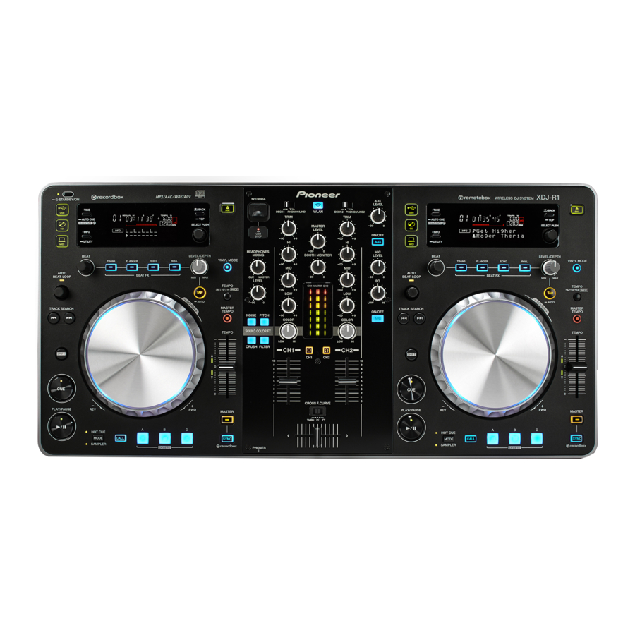
Pioneer XDJ-R1 Service Manual
Dj system
Hide thumbs
Also See for XDJ-R1:
- Quick start manual (84 pages) ,
- Operating instructions manual (38 pages) ,
- Operation manual (19 pages)
Table of Contents
Advertisement
Quick Links
DJ SYSTEM
XDJ-R1
THIS MANUAL IS APPLICABLE TO THE FOLLOWING MODEL(S) AND TYPE(S).
Model
Type
XDJ-R1
SVWYXE8
XDJ-R1
CUXE
XDJ-R1
FLWPWXE
XDJ-R1
KXE5
XDJ-R1
AXE5
PIONEER CORPORATION
PIONEER ELECTRONICS (USA) INC. P.O. Box 1760, Long Beach, CA 90801-1760, U.S.A.
PIONEER EUROPE NV Haven 1087, Keetberglaan 1, 9120 Melsele, Belgium
PIONEER ELECTRONICS ASIACENTRE PTE. LTD. 253 Alexandra Road, #04-01, Singapore 159936
PIONEER CORPORATION
Power Requirement
AC 220 V to 240 V
AC 120 V
AC 110 V to 120 V or 220 V to 240 V
AC 220 V
AC 220 V to 240 V
1-1, Shin-ogura, Saiwai-ku, Kawasaki-shi, Kanagawa 212-0031, Japan
2013
XDJ-R1
K-MZV JUNE
ORDER NO.
RRV4401
Remarks
2013 Printed in Japan
Advertisement
Table of Contents

Related Manuals for Pioneer XDJ-R1


Summary of Contents for Pioneer XDJ-R1
- Page 1 PIONEER CORPORATION 1-1, Shin-ogura, Saiwai-ku, Kawasaki-shi, Kanagawa 212-0031, Japan PIONEER ELECTRONICS (USA) INC. P.O. Box 1760, Long Beach, CA 90801-1760, U.S.A. PIONEER EUROPE NV Haven 1087, Keetberglaan 1, 9120 Melsele, Belgium PIONEER ELECTRONICS ASIACENTRE PTE. LTD. 253 Alexandra Road, #04-01, Singapore 159936...
-
Page 2: Safety Information
A SPECIALLY INSTRUCTED PERSON SHOULD DO SERVICING OPERATION OF THE APPARATUS. LASER DIODE CHARACTERISTICS For CD Wave length : 775 - 800 nm Output Power : Less than Class 1 LABEL CHECK for SVWYXE8 for CUXE for FLWPWXE for KXE5 for AXE5 XDJ-R1... -
Page 3: Table Of Contents
11.3 DSP & POWER ASSY ..............................68 11.4 CH, CROSS FADER, USB and PHONES ASSEMBLIES................... 70 11.5 Wi-Fi PCB ASSY ................................ 71 11.6 CD1 and CD2 ASSEMBLIES............................72 11.7 SERVO ASSY ................................74 11.8 SWITCHING POWER..............................75 12. PCB PARTS LIST ................................76 XDJ-R1... -
Page 4: Service Precautions
Compared with eutectic solders, lead-free solders have higher bond strengths but slower wetting times and higher melting temperatures (hard to melt/easy to harden). The following lead-free solders are available as service parts: • Parts numbers of lead-free solder: GYP1006 1.0 in dia. GYP1007 0.6 in dia. GYP1008 0.3 in dia. XDJ-R1... -
Page 5: Specifications
• CD-ROM (The disc includes rekordbox, the driver software, the LOW — CENTER — HI..–12 dB (10 kHz) to 0 dB to –12 dB (100 Hz) XDJ-R1’s operating instructions and the operating instructions for remotebox. The rekordbox license key is attached.) (429-COMBO-144) •... -
Page 6: Basic Items For Service
It must be confirmed that music files playbacked in the PC can be transferred to the XDJ-R1 via wireless LAN, using rekordbox installed rekordbox Supplied software on the PC. You can download rekordbox from the Pioneer Web site. Lubricants and Glues List Name Part No. -
Page 7: Pcb Locations
MIXER ASSY 704-COMBO-A376 SWITCHING POWER 411-COMBO-887 CH ASSY 704-COMBO-A482 CROSS FADER ASSY 704-COMBO-A499 SLOT-IN FEEDER MECHA ASSY 704-MCU300-9997-HA USB ASSY 704-COMBO-A381 PHONES ASSY 704-COMBO-A379 DSP & POWER ASSY 704-COMBO-A531 Wi-Fi PCB ASSY 704-COMBO-A380 CD1 ASSY 704-COMBO-A375 CD2 ASSY 704-COMBO-A476 XDJ-R1... -
Page 8: Block Diagram
11. GND 1. Q1 2. SL+ 12. +6V/V5 2. Q2 AC IN 3. Disc Detecting Switch 13. +6V/V5 3. DGND 4. S3.3V 14. STBY:5V->Power ON SERVO ASSY W203 (704-COMBO-A377) PHONES ASSY 1. L 2. G (704-COMBO-A379) 3. G 4. R XDJ-R1... - Page 9 LMA (BROWN) 13. VR LMB (BLACK) 14. FC- MOTOR SP- (BLUE) 15. TC- SP+ (RED) 16. TC+ 17. FC+ 1. Q1 2. Q2 CN105 3. DGND 1. SL- 2. SL+ 3. Disc Detecting Switch CN106 4. S3.3V SERVO ASSY (704-COMBO-A377) XDJ-R1...
-
Page 10: Overall Block Diagram
6V/4A,+15V&- 15V/0.4A,7V/2A CD DSP BUCK STB5V/0.2A,32V/0.35A Opitical AC Plug +Ef&- Ef(3.4V/0.8A) -15V BD4745 Com pare STB5V IC103 Load CD Driv er UI MCU BA6218 Motor OP A Motor Driver Power Delay +15V Disc Sensor DSP & POWER TP S54 ASSY XDJ-R1... - Page 11 AD3.3V_1 CD ASSY MCU,PLL,Logic,VFD BUCK IC816 BU33TD3 BD4745 BA05 AD3.3V_2 Com pare IC817 BU33TD3 Power USB Host Delay min.1100mA BA05 TP S2553 Curr.L TD DSP,SDRAM,Wi-Fi, D3.3V D1.2V USB IF,Servo Driver, IC407 FlashRom DSP Core TP S54232 BD12K A BUCK XDJ-R1...
-
Page 12: System Block Diagram
AUX ON/OFF IC404 MIC Input level MIC ON/OFF MIC mono IC406 6.4mm USB IN1 USB Audio IN1 USB Audio Mix USB IN2 USB Audio IN2 USB Audio HP USB Audio IN USB Audio OUT USB PortB USB MASTER OUT XDJ-R1... - Page 13 CH1 CUE BALANCE MASTER TRIM MASTER(XLR) IC409 TRANS COLOR ECHO FLANGER EFFECT EFFECT EFFECT MASTER2(RCA) BOOTH TRIM IC410 BOOTH(RCA) LEVEL Meter MAS CH2 CH2 CUE Phones JACK IC411 6.4mm TRANS ECHO COLOR FLANGER EFFECT EFFECT 3.5mm MASTER/CUE HP LEVEL EFFECT XDJ-R1...
-
Page 14: Level Block Diagram
Max. MIC Level DSP Gain -50dBV +9.9 Phono Level -54dBV MI C Level DR:103dB Phono Noise -96.05dBV -100 -100 -100 -110 -110 MI C Noise -113.1dBV -110 -120 -120 -120 @- 123dBV Noise Level -130 -130 -130 -144dBF S@24bit -140 XDJ-R1... - Page 15 Unbalance Out 0dBu(Ref.) +16.8 AUX Boost -15.55dBV 100%position Unbalance Out - 14dBV -20.76dBF S 80%position -29.55dBV -32.55dBF S 80%position DR:105.24dB MIC@- 68.78dBV Phono@- 72.77dBV DSP -->DA@- 87.41dBV -100 -100 -100 -110 -110 -110 -120 -120 -130 -130 dBF S@24bit XDJ-R1...
-
Page 16: Diagnosis
C802 (CROSSFADER), C807 (CH1 FADER), C806 (CH2 FADER) that positive to ground is VR out. Waveform for min VR out is figure (Waveform Waveform for max VR out is figure (Waveform 2. If Waveform is abnormal, you could change it. XDJ-R1... - Page 17 Symptom: The USB audio not activated. Diagnostic procedure: 1. Check Waveform for I/O Assy IC400 pin 35 (LRCK)(Waveform ), pin 34 (BCK)(Waveform 10-1 10-2 pin 44 (MCLKO)(Waveform ), you confirm it is correct. 10-3 2. If Waveform is abnormal, you could change it. XDJ-R1...
- Page 18 1. Check Waveform for I/O Assy IC406 pin 15 (SCK)(Waveform ), pin 11 (BCK)(Waveform 14-1 14-2 pin 10 (LRCK)(Waveform ), pin 12 (DOUT)(Waveform ), you confirm it is correct. 14-3 14-4 2. If Waveform is abnormal, you could change it. XDJ-R1...
-
Page 19: Confimation Of Wireless Lan Communication
1 On the top screen of an iPod touch, select Settings. 2 Select Wi-Fi (Not Connected) 3 Check that the SSID selected of this unit is displayed in the "Choose a Network" box. Check that the SSID selected of this unit is displayed. XDJ-R1... -
Page 20: Error Code List
• Communication of "UI Ucom" and "DSP" cannot be is established between the UI Ucom and DPS, performed. because of inappropriate connection, etc. ERROR at the time of POWER ON. E-9101 MECHANICAL TIMEOUT • A mechanical operation could not be completed within the specified time. XDJ-R1... -
Page 21: Service Mode
• TIME display mode starts from the DECK VOL display mode. • When the TEMPO slider is moved far down to the [+] side during this mode, the mode is switched to JOG dial load measurement mode. : (1) Time display : (2) : (3) Dot display XDJ-R1... - Page 22 SOUND COLOR FX (PITCH) indicator ————— SOUND COLOR FX (FILTER) button FILTER SOUND COLOR FX (FILTER) indicator ————— SOUND COLOR FX (NOISE) button NOISE SOUND COLOR FX (NOISE) indicator ————— SOUND COLOR FX (CRUSH) button CRUSH SOUND COLOR FX (CRUSH) indicator ————— XDJ-R1...
- Page 23 0 to FF (in SEC of TIME display) ————— Always on TIME display VFD. Crossfader 0 to FF (in FRAME of TIME display) ————— Always on TIME display VFD. Channel fader (CH2) 0 to FF (in TEMPO number display) ————— Always on TIME display VFD. XDJ-R1...
- Page 24 • A track displayed is searched clockwise or counterclockwise and paused. Eject (DISC h) • A Disc is ejected. Mode Change (MASTER TEMPO) • When the MASTER TEMPO button is pressed in the CD drive performance mode, the MASTER TEMPO's LED lights up and shifted to Test performance mode. XDJ-R1...
- Page 25 • When the CALL button is pressed, the following versions are toggled to be displayed. (1) Ver. 1.00 SYSTEM version ↓ (2) DSP 1.00 DSP version ↓ (3) SERVO 1.00 SERVO version ↓ (4) MIXER 1.00 MIXER version ↓ (5) CON 1.00 UI version ↓ (6) VFD 1.00 VFD version XDJ-R1...
- Page 26 PITCH2_1 PITCH1_2 PITCH2_2 DEPTH_1 DEPTH_2 CH1_TRIM CH2_TRIM CH1_HI CH2_HI CH1_MID CH2_MID The VR name that is indicated Maximum value CH1_LOW CH2_LOW CH1_FILTER CH2_FILTER CH1_FADER CH2_FADER H.P.LEVEL AUX LEVEL H.P..MIXING MIC LEVEL CROSS FADER MIC EQ MASTER LEVEL BOOTH MONITOR XDJ-R1...
-
Page 27: Factory Reset
Wi-Fi related: It is the same as that of the case where YES TIME MODE : REMAIN of UTILITY (WLAN) RESET TO DEFAULT is chosen. AUTO CUE : OFF MIXER MODE : XDJ-R1 TEMPO RANGE : ±10 % A.CUE LEVEL : -60 dB MASTER TEMPO : OFF... -
Page 28: Disassembly
(2) Even if the unit shown in the photos and illustrations in this manual may differ from your product, the procedures described here are common. Knobs and Volumes Location 100-COMBO-2962 100-DJM100-2826-HA 100-DJM250-2826-HA 100-CMX4-2906-HA 100-22-2824-HA ×6 ×4 ×15 ×2 ×3 White White White White Black Gray Black Black Black White White XDJ-R1... - Page 29 • Bottom view (3) Remove the Control panel Section. (4) Disconnect the three flexible cables and three Control panel Section connectors. (CN200, 209, 210, 804, 812A, 812B) MIXER Assy ×3 CN209 CN210 CN200 ×3 CN804 CN812A CN812B DSP & POWER Assy XDJ-R1...
- Page 30 MECHA Assy (DECK1) MECHA Assy (DECK2) [2-3] SERVO Assy (1) Disconnect the one flexible cable and two connectors. (CN101, 105, 106) (2) Remove the four screws. (602-DD2220-301) (3) Remove the SERVO Assy. CN101 CN105 CN106 • Bottom view SERVO Assy XDJ-R1...
- Page 31 (3) Remove the top cover. Top cover Pickup lens Caution: Work not to transform two springs. Caution Caution Cleaning the pickup lens Clean the pickup lens when it is stained, using the following cleaning materials: Cleaning liquid : GEM1004 Cleaning paper: GED-008 XDJ-R1...
- Page 32 • Method to perform forced ejection of a disc Turn the gear pulley to the arrow direction of the figure with finger. Gear pulley The disc comes out when you continue turning gear pulley. Disc Gear pulley Pull out the disc out by hand. Gear pulley Disc XDJ-R1...
- Page 33 (4) Remove the two screws. (602-ISO308-735B) (5) Remove the eight screws. (602-PTS308-732B) (6) Remove the two screws. (602-SA12-377) (7) Remove the one screw. (602-SA12-380) (8) Remove the I/O Assy. I/O Assy Screw tightening order The other screws are random order. XDJ-R1...
- Page 34 (4) Remove the Front panel Assy Section by removing the 10 screws. (602-SL24F-099) ×10 • Rear view PHONES Assy Front panel Assy Section (5) Remove the PHONES Assy by removing the three screws. PHONES Assy (602-DV300-5023) • Rear view ×3 Screw tightening order 2 1 3 XDJ-R1...
- Page 35 (602-STS2003-677) (6) Remove the Wheel ring Assy by removing the Wheel reactor six screws. (602-A700-494) (7) Remove the Wheel reactor by removing the ×6 six screws. (602-A700-494) Wheel ring Assy Screw tightening order Spring Wheel outer ring Wheel plate XDJ-R1...
- Page 36 CH Assy the two screws. (602-SA12-380) (9) Disconnect the one connector. (CN01) (10) Remove the Fixed plate by removing the CROSS FADER Assy two screws. (602-SA12-414) ×2 CH fixed plate Fixed plate ×2 CN01 CN208 CH Assy CROSS FADER Assy XDJ-R1...
- Page 37 (4) Remove the two screws and two washers. (602-MK8-604) (5) Release the jumper wires. CN204 (6) Remove the four screws. (602-MK8-604) (7) Remove the CD1 and 2 Assemblies by removing the 43 screws. • Bottom view (602-MK8-604) CD2 Assy CD1 Assy XDJ-R1...
- Page 38 (GYL1005) Grease (GEM1072) Bottom • Bottom view side Bottom Bottom side side Bottom Bottom side side Chassis Assy Adhesive Adhesive (GYL1001) (GYL1001) SLOT-IN FEEDER Adhesive MECHA Assy SERVO Assy (GYL1005) Grease (GEM1072) Adhesive Adhesive (GYL1005) (GYL1001) • Bottom view XDJ-R1...
-
Page 39: Each Setting And Adjustment
(As for the Wi-Fi PCB Assy, the SSID will be changed when resetting to factory default is performed after replacement.) When returning the repaired product to the customer, be sure to tell the customer that resetting of the wireless LAN connection will be required. XDJ-R1... -
Page 40: Updating Of The Firmware
• If the firmware update is failed in such a case as turning off the power in the middle of the update, any subsequent control is not available. • When Error code E-7024 appears, recovery mode starts to continue the update again if appropriate USB update procedures are taken. XDJ-R1... -
Page 41: User Setable Items
CH1 — 11, AUTO DHCP SERVER ENABLE / DESABLE MIXER MODE XDJ-R1 / PC UTILITY settings –36 dB / –42 dB / –48 dB / –54 dB / A. CUE LEVEL –60 dB / –66 dB / –72 dB / –78 dB SAMPLE LEVEL 1 —... -
Page 42: Exploded Views And Parts List
For the applying amount of lubricants or glue, follow the instructions in this manual. (In the case of no amount instructions, apply as you think it appropriate.) 9.1 PACKING SECTION SVWYXE8, FLWPWXE only for SVWYXE8, CUXE, for FLWPWXE KXE5, AXE5 SVWYXE8, FLWPWXE only XDJ-R1... - Page 43 See Contrast table (2) 17 About SSIDs and Passwords 501-XJR1-2506 18 Label See Contrast table (2) (2) CONTRAST TABLE XDJ-R1/SVWYXE8, CUXE, FLWPWXE, KXE5 and AXE5 are constructed the same except for the following: XDJ-R1 XDJ-R1 XDJ-R1 XDJ-R1 XDJ-R1 Mark No. Symbol and Description...
-
Page 44: Exterior Section
Wheel reactor (NSP) (NSP) Screw (NSP) EVA sheet (NSP) EVA sheet (NSP) EVA sheet (NSP) EVA sheet Note: (NSP) EVA sheet and Gascket do not supply it for service parts. These are put on service parts of PCB Assy. XDJ-R1... - Page 45 Note: EVA sheet and Gascket do not supply it for service parts. These are put on service parts of PCB Assy. Gascket Ferrite core (NSP) (NSP) Gascket (NSP) Gascket (NSP) Ferrite core (NSP) Safety label (NSP) XDJ-R1...
- Page 46 41 • • • • • 87 Transfer Plate 300-COMBO-2034 42 Electrical Tape 501-COMBO-2216 88 Mecha Fixed Plate 300-COMBO-2036 43 Canoe Clips (MB-1S) 504-HF6011-5011 89 CH Fixed Plate 300-COMBO-2038 44 Fixed Loop (2A-8) 504-COMBO-300 90 Ground Plate L 300-COMBO-2064 45 Spacer Support 504-QFX-204 XDJ-R1...
- Page 47 127 Screw 602-SA12-380-HA 128 Screw 602-SA12-414 129 Screw 602-SL24F-099 130 Screw 602-ST150-431 (2) CONTRAST TABLE XDJ-R1/SVWYXE8, CUXE, FLWPWXE, KXE5 and AXE5 are constructed the same except for the following: XDJ-R1 XDJ-R1 XDJ-R1 XDJ-R1 XDJ-R1 Mark No. Symbol and Description /SVWYXE8...
-
Page 48: Schematic Diagram
33(8P4R) RB405 RB407 10/25 R478 C456 C449 LRCK 3 L412 Bead C897 C935 C898 C936 C899 C937 100/10 C451 RB423 100P 100P 100P 14-3 14-2 33(8P4R) ADDA EM638165TS- 6G C510 EM638165TS- 6G C514 RB421 33(8P4R) 33(8P4R) 33(8P4R) /XST 14-4 XDJ-R1... - Page 49 AD16 AD17 DO10 AD15 AD18 CN810 AD10 SPI SCK" AD16 CN210 SPI MOSI/MI SO AD17 SPI CS" CD1 SCOR1 AD18 /RST- 532 CD2 SCOR2 AD10 SPI HREQ SPI RTS UTX" SAD3.3V SADGND FFC 26P C895 C896 0.1(NC) 0.1(NC) Title XDJ-R1...
-
Page 50: Mixer, Ch, Cross Fader, Usb And Phones Assemblies
AD16 SADGND CH ASSY (CH1) SAD3.3V 20K B K S1 AD17 (704-COMBO-A482) K S2 CH1 Fader AD18 K S3 K S4 K S5 AD10 CN208 W208B VR218 AD15 CH ASSY (CH2) 20K B (704-COMBO-A482) CH2 Fader B C D XDJ-R1... - Page 51 AD15 1000P JK 201 DGND C269 ACM2012 C271 /PB1 CHASSIS 1000P R344 /PB1 1000P /PA1 CHASSIS 2.7K /PA1 D249 C251 R347 R348 D248 C252 USB A(HOST) PHONES OUT EDZC6.8B 0.01 EDZC6.8B 10/25 3.5mm USB ASSY PHONES ASSY (704-COMBO-A381) (704-COMBO-A379) XDJ-R1...
-
Page 52: Dsp & Power Assy (1/2) And Wi-Fi Pcb Assy
SPI CS" L822 BEAD(300) R885 CD1 SCOR1 L829 BEAD(300) R907 /RST- 532 L830 BEAD(120) CD2 SCOR2 L831 BEAD(120) R908 /PB1 SPI HREQ L832 BEAD(120) R886 /PB1 /PA1 SPI RTS L833 BEAD(120) /PA1 BEAD(120) R889 R890 UTX" L834 BEAD(120) FFC 26P XDJ-R1... - Page 53 INT0 4D10 R922 1D10 WF TXD XDATA2 TXD0 C881 BURN_EN WF RXD R923 XDATA4 RXD0 CN806 BURN_921K XDATA5 R924 R882 XDATA6 /PB1 /WRST 4.7K (NC) /PB1 RST_N /PA1 /PA1 R890 R881 WSCK 4.7K D_MI SO D_MOSI C925 Shield cable XDJ-R1...
-
Page 54: Dsp & Power Assy (2/2)
ADDA MUTE /MST Bead RRR030P 03 +15V 0.47(M) 100/25 A+15V ST5V A- 15V 100/25 C124EK A Bead 470/16(L ) 0.47(M) TP S2553 -15V Bead A- 15V ILIM RTR030N05 /FAULT 220/16 21K ,1% min.1100mA 2SA1037AK V- CHK V- CHK UGND XDJ-R1... - Page 55 V- CHK D3.3V A- 15V ADDA SM5819A 100K MUTE MUTE 100K A124TK A /MST A+15V /MST 1SS355 RRR030P 03 3.3K 0.47(M) 22/16 330/16 A- 15V STBY Close C47 STBY C124EK A 0.47(M) C124EK A BD4745G A- 15V 1SS355 RTR030N05 22/16 XDJ-R1...
-
Page 56: Cd1 And Cd2 Assemblies
10.5 CD1 and CD2 ASSEMBLIES D SO 6/3 D SO 3/4 G N D SC K V C C /O E 1 D SO 3/4 D SO 5/6 G N D SC K V C C /O E 1 CN204 (DECK2) CN201 XDJ-R1... - Page 57 E N 5 E N 6 SW 130 K S2 L O O P K S3 K S4 ST B -SW K S5 A D 1/5 A D 2/6 A D 3/7 7-1 7-2 A D 4/8 CN201 (DECK1) XDJ-R1...
-
Page 58: Servo Assy
MECHA R107 47/16(CF ) R106 AVDD1 R105 33K C107 R104 R101 R102 L101 4.7K C102 C101 100/10(CF ) C126 C105 Q101 TP 2 17P FFC 680P 2SA1037 100/10(CF ) C171 S3.3V TP 1 TP 3 R103 1000 L102 S3.3V XDJ-R1... - Page 59 1000P 1000P DVDD CHASSI S CHASSI S CHASSI S CHASSI S C130 R177 X102 16.934M C134 C136 C164 C168 C129 R178 1000P 1000P 1000P 1000P CHASSI S CHASSI S CHASSI S CHASSI S CHASSI S CHASSI S C171 1000P XDJ-R1...
-
Page 60: Switching Power
MMBTA94 2Ω 10uF/35V S13003 10Ω 1N4148 IC FAN6754MR 470pF/1KV HER303 R8 10Ω 33Ω GATE 1N4937 10K Ω R11 1K Ω SENSE R23 10Ω IC5B IC1B SR3100 1nF/50V 0.13Ω 330PF/50V LTV817 LTV817 100K Ω 470pF/1KV R25 10Ω 1000pF/250V 0.1uF 470uF/10V XDJ-R1... - Page 61 56K Ω R23 10Ω 220uF/50V '0V'->Only ST5V Power ON Others Power OFF SR3100 10nF 100K Ω /1KV 4*15 4.7uH +Ef 3.4V /V7 0Ω SP1482 10uF 10uF COMP 27K Ω 0.1uF 10K Ω 0.1uF 470uF/10V 3.3nF 100uF/16V 0.1uF R52 6.8K Ω XDJ-R1...
-
Page 62: Waveforms
CH2: Q101 pin C) -15V LED ON Min VR without touch (C24 negative) (Q102 to Q112 pin C) (C802, C807, C806 positive) (C113) LED OFF Max VR touch (C21 positive) (Q102 to Q112 pin C) (C802, C807, C806 positive) (C113) XDJ-R1... - Page 63 10 (DISC SW2 (CH4))) 11-112-113-114-1 13-4 Insert disc DATA (CN102A pin 12 (CLSW (CH2)), pin 11 (OPSW (IC411 pin 2) (CH3)), pin 9 (DISC SW1 (CH1)), (IC409 to IC411 pin 16, IC406 pin 15) pin 10 (DISC SW2 (CH4))) XDJ-R1...
-
Page 64: Pcb Connection Diagram
SIDE A CN200 CN810 CN810 CN210 CN200 CN210 10-3 10-1 10-2 IC400 Q403 Q402 Q401 Q405 Q406 IC416 IC812 IC413 IC408 IC418 IC417 IC415 IC419 SIDE B CN810 CN210 CN200 IC808 IC809 IC414 IC407 IC402 IC401 IC403 IC412 Q404 XDJ-R1... - Page 65 2. View point of PCB diagrams. Connector Capacitor SIDE A SIDE B P.C.Board Chip Part 14-1 14-3 14-2 14-4 IC407 IC404 IC406 IC410 Q429-Q432 IC409 Q428 IC423 Q404 IC405 Q421 IC424 Q422 Q407 IC422 Q408 Q413-Q416 Q417-Q420 Q423-Q426 Q409-412 XDJ-R1...
-
Page 66: Mixer Assy
11.2 MIXER ASSY SIDE A SIDE A MIXER ASSY CN209 CN210 CN200 IC209 Q218 IC208 IC203 Q202 Q204 IC205 Q219 Q201 W208A W208B W203 CN208 (CH1) CN208 (CH2) CN01 XDJ-R1... - Page 67 SIDE B SIDE B MIXER ASSY CN200 CN210 CN209 CN200 CN210 CN209 IC207 Q217 Q200 IC200 Q209 Q210 Q211 Q212 IC202 Q213 Q214 Q215 Q208 Q216 Q207 XDJ-R1...
-
Page 68: Dsp & Power Assy
11.3 DSP & POWER ASSY SIDE A W812 CN810 CN209 W205 CN810 CN209 CN804 (DECK1) DSP & POWER ASSY SIDE B DSP & POWER ASSY W402B CN810 CN806 CN810 CN209 CN804 XDJ-R1... - Page 69 SIDE A W812 W812 CN812A CN812B (DECK1) (DECK2) IC816 IC806 IC802 IC813 IC814 SIDE B IC801 IC803 Q3-Q6 IC805 Q801 IC815 Q800 Q804 Q803 CN812A CN812B XDJ-R1...
-
Page 70: Ch, Cross Fader, Usb And Phones Assemblies
CROSS FADER ASSY CH ASSY CN01 CN208 W208A (CH1), W208B (CH2) USB ASSY PHONES ASSY W203 W205 CN401 CN804 SIDE B SIDE B PHONES ASSY USB ASSY W203 W205 CH ASSY CN208 CROSS FADER ASSY CN01 C D E F W203 XDJ-R1... -
Page 71: Wi-Fi Pcb Assy
11.5 Wi-Fi PCB ASSY SIDE A SIDE A Wi-Fi PCB ASSY IC811 W811 IC810 W806 SIDE B SIDE B Wi-Fi PCB ASSY XDJ-R1... -
Page 72: Cd1 And Cd2 Assemblies
11.6 CD1 and CD2 ASSEMBLIES SIDE A SIDE A CD1 ASSY CN812A (DECK1) CN206A (DECK1) CN201 (DECK1) CN812B (DECK2) CN206B (DECK2) CD2 ASSY CN201 W812 W206 3-1 3-2 IC102 Q106-Q112 Q100-Q102 Q103 Q104 IC101 Q105 IC103 IC104 CN204 CN204 (DECK2) XDJ-R1... - Page 73 SIDE B SIDE B CD1 ASSY CD2 ASSY W206 W812 CN201 CN204 XDJ-R1...
-
Page 74: Servo Assy
11.7 SERVO ASSY SIDE A To MOTOR SIDE A SERVO ASSY MECHA MECHA IC102 IC228 IC104 Q105 Q104 IC103 Q103 CN102A CN106 CN808 (DECK1) CN809 (DECK2) To MECHA SIDE B SIDE B CN106 CN102A Q106 Q101 Q102 SERVO ASSY XDJ-R1... -
Page 75: Switching Power
11.8 SWITCHING POWER SIDE A SIDE A SWITCHING POWER AC IN SIDE B SIDE B SWITCHING POWER XDJ-R1... -
Page 76: Pcb Parts List
415-MC6000-356 L 201 POWER CHOKE 415-MC6000-356 L 818 CHIP BEAD 415-1300-240A L 202 INDUCTOR (10 uH T-26MM) 415-MPG100-047-HA SW 400-402 SLIDE SW 403-COMBO-427 SW 200,205,207 TACT SW 403-DDJLE-419-HA SW 211 SLIDE SW 403-DMX101-393 W6 TO IC 3P WIRE 404-K1000-2636 XDJ-R1... - Page 77 415-VP9812-221-HA C 3,4,861-863,868,869,920 CHIP CAPACITOR 413-MC6000-1180 C 921,926,927,929,931 CHIP CAPACITOR 413-MC6000-1180 C 31,871 CAPACITOR 413-MC6000-1190 C 866,867 ELEC.CAPACITOR 413-MC6000-1191-HA DSP & POWER ASSY C 37 ELEC.CAPACITOR 413-HP1010K-200-HA SEMICONDUCTORS C 21,858 ELEC.CAPACITOR 413-HMA2200-5017-HA TRANSISTOR 416-FU800-367 C 42 ELEC. CAPACITOR 413-COMBO-1257 XDJ-R1...
- Page 78 Q 104,105 CHIP TRANSISTOR 416-CDN88-051 D 102,103 INFRARED EMITTONG 410-CDMIX1-147 CAPACITORS C 112,120 ELEC. CAPACITOR 413-SPPW3-235-HA MISCELLANEOUS C 115 ELEC.CAPACITOR 413-HMA2200-5017-HA C 128,129,131 CHIP CAPACITOR 413-MC6000-1180 CN 101 17P SOCKET 404-MCU300-3615-HA C 139 ELEC. CAPACITOR 413-DM1000-348 CN 106 3P SOCKET 404-HMD5000-784A-HA XDJ-R1...
- Page 79 C 110 CHIP ELEC. CAPACITOR 413-45X-1243 C 114,128,132 CHIP ELEC. CAPACITOR 413-45X-1242 C 102,103,105,121,125 CHIP ELEC. CAPACITOR 413-45X-1241 C 151,157-160 CHIP ELEC. CAPACITOR 413-45X-1241 C 112 ELEC. CAPACITOR 413-SPPW3-305 C 113 CHIP ELEC. CAPACITOR 413-COMBO-1254 C 106,123 CHIP ELEC. CAPACITOR 413-COMBO-1253 XDJ-R1...