Table of Contents
Advertisement
DVD PLAYER
DV-757Ai
DV-S755Ai
THIS MANUAL IS APPLICABLE TO THE FOLLOWING MODEL(S) AND TYPE(S).
Model
Type
DV-757Ai
WYXJ
DV-S755Ai
RLXJ/NC
For details, refer to "Important symbols for good services".
PIONEER CORPORATION
PIONEER ELECTRONICS (USA) INC. P.O. Box 1760, Long Beach, CA 90801-1760, U.S.A.
PIONEER EUROPE NV Haven 1087, Keetberglaan 1, 9120 Melsele, Belgium
PIONEER ELECTRONICS ASIACENTRE PTE. LTD. 253 Alexandra Road, #04-01, Singapore 159936
PIONEER CORPORATION 2002
Power Requirement
AC220-240V
AC110-127V/220-240V
4-1, Meguro 1-chome, Meguro-ku, Tokyo 153-8654, Japan
DV-757Ai
Regional restriction
codes (Region No.)
2
3
T-ZZE SEPT. 2002 printed in Japan
ORDER NO.
RRV2668
Remarks
Advertisement
Table of Contents

Related Manuals for Pioneer DV-S755AI


Summary of Contents for Pioneer DV-S755AI
-
Page 1: Dvd Player
PIONEER CORPORATION 4-1, Meguro 1-chome, Meguro-ku, Tokyo 153-8654, Japan PIONEER ELECTRONICS (USA) INC. P.O. Box 1760, Long Beach, CA 90801-1760, U.S.A. PIONEER EUROPE NV Haven 1087, Keetberglaan 1, 9120 Melsele, Belgium PIONEER ELECTRONICS ASIACENTRE PTE. LTD. 253 Alexandra Road, #04-01, Singapore 159936 PIONEER CORPORATION 2002 T-ZZE SEPT. -
Page 2: Safety Information
SAFETY INFORMATION This service manual is intended for qualified service technicians; it is not meant for the casual do-it-yourselfer. Qualified technicians have the necessary test equipment and tools, and have been trainedto properly and safely repair complex products such as those covered by this manual. Improperly performed repairs can adversely affect the safety and reliability of the product and may void the warranty. - Page 3 [ Important symbols for good services ] In this manual, the symbols shown-below indicate that adjustments, settings or cleaning should be made securely. When you find the procedures bearing any of the symbols, be sure to fulfill them: 1. Product safety You should conform to the regulations governing the product (safety, radio and noise, and other regulations), and should keep the safety during servicing by following the safety instructions described in this manual.
-
Page 4: Table Of Contents
CONTENTS SAFETY INFORMATION ............................. 2 1. SPECIFICATIONS ............................5 2. EXPLODED VIEWS AND PARTS LIST ......................8 2.1 PACKING ..............................8 2.2 EXTERIOR SECTION..........................10 2.3 FRONT PANEL SECTION ........................12 2.4 LOADING MECHA ASSY ........................14 2.5 TRAVERSE MECHANISM ASSY-S ......................16 3. -
Page 5: Specifications
1. SPECIFICATIONS 7 DV-757Ai/WYXJ • Manufactured under license from Dolby Laboratories. “Dolby” and the double-D symbol are trademarks of Dolby Laboratories. • “DTS” is a registered trademark of Digital Theater Systems, Inc. • TruSurround and the ® symbol are trademarks of SRS Labs, Inc. TruSurround technology is incorporated under license from SRS Labs, Inc. - Page 6 7 DV-S755Ai/RLXJ/NC • Manufactured under license from Dolby Laboratories. “Dolby” and the double-D symbol are trademarks of Dolby Laboratories. • “DTS” is a registered trademark of Digital Theater Systems, Inc. • TruSurround and the ® symbol are trademarks of SRS Labs, Inc. TruSurround technology is incorporated under license from SRS Labs, Inc.
- Page 7 DV-757Ai...
-
Page 8: Exploded Views And Parts List
2. EXPLODED VIEWS AND PARTS LIST NOTES: Parts marked by "NSP" are generally unavailable because they are not in our Master Spare Parts List. mark found on some component parts indicates the importance of the safety factor of the part. Therefore, when replacing, be sure to use parts of identical designation. - Page 9 See Contrast table (2) Polyethylene Bag VHL1051 (Trad-Chinese) Pad F VHA1311 Pad R VHA1312 (2) CONTRAST TABLE DV-757Ai/WYXJ and DV-S755Ai/RLXJ/NC are constructed the same except for the following: DV-S755Ai/ Mark No. Symbol and Description DV-757Ai/WYXJ RLXJ/NC > 1 Power Cable ADG7053...
-
Page 10: Exterior Section
2.2 EXTERIOR SECTION NON-CONTACT SIDE CONTACT SIDE Refer to "2.4 LOADING MECHA ASSY". No.7, No.15: WYXJ Type Only *1: Be just connected. No.8 (AC Inlet Assy) → CN1 No.22 (Housing Assy) → CN2 WYXJ Type Only Refer to "2.3 FRONT PANEL SECTION". DV-757Ai... - Page 11 NSP 63 ID Label VRW1877 PCB Holder See Contrast table (2) PCB Holder VEC2283 (2) CONTRAST TABLE DV-757Ai/WYXJ and DV-S755Ai/RLXJ/NC are constructed the same except for the following: DV-S755Ai/ Mark No. Symbol and Description DV-757Ai/WYXJ RLXJ/NC 1 DVDM Assy VWS1540...
-
Page 12: Front Panel Section
2.3 FRONT PANEL SECTION 8 (1/2) 8 (2/2) NON-CONTACT SIDE CONTACT SIDE DV-757Ai... - Page 13 Pioneer Badge See Contrast table (2) NSP 11 LED Lens 2 VNK5105 FL Filter VEC2281 (2) CONTRAST TABLE DV-757Ai/WYXJ and DV-S755Ai/RLXJ/NC are constructed the same except for the following: DV-S755Ai/ Mark No. Symbol and Description DV-757Ai/WYXJ RLXJ/NC 1 FLKY Assy VWG2358...
-
Page 14: Loading Mecha Assy
2.4 LOADING MECHA ASSY Note : DVDM Refer to CN101 " Application of Lubricant". To DVDM CN114 Daifree To DVDM CN115 GEM1036 Refer to "2.5 TRAVERSE MECHANISM ASSY-S". Lubricating Oil GYA1001 Lubricating Oil GYA1001 LOADING MECHA ASSY parts List Mark No. Description Part No. - Page 15 Application of Lubricant Lubricating Oil GYA1001 Around the shaft No. 11 Loading Base Lubricating Oil GYA1001 Lubricating Oil GYA1001 No. 13 Lubricating Oil Drive Cam GYA1001 No. 13 Top View Drive Cam Rear View Inner side of a ditch Inner side of a ditch Lubricating Oil Lubricating Oil GYA1001...
-
Page 16: Traverse Mechanism Assy-S
2.5 TRAVERSE MECHANISM ASSY-S 17 (Torque : 0.12 ± 0.01 N•m) Silicone Adhesive GEM1037 Silicone Adhesive GEM1037 4 (Adjustment Screw) 17 (Torque : 0.12 ± 0.01 N•m) DVDM CN111 Screw Tight Silicone Adhesive GYL1001 GEM1037 To DVDM 17 (Torque : 0.12 ± 0.01 N•m) CN115 To DVDM CN114... - Page 17 TRAVERSE MECHANISM ASSY-S parts List Mark No. Description Part No. Spindle Motor VXM1088 Stepping Motor VXM1090 > Pickup Assy-S OXX8004 Skew Screw VBA1080 Skew Spring VBH1335 Guide Bar VLL1514 Sub Guide Bar VLL1515 Hold Spring VNC1017 Joint Spring VNC1019 Support Spring VNC1020 NSP 11 Mechanism Chassis...
-
Page 18: Block Diagram And Schematic Diagram
3. BLOCK DIAGRAM AND SCHEMATIC DIAGRAM 3.1 BLOCK DIAGRAM 7 SIGNAL ROUTE i.LINK ILKB ASSY CN902 12 14 16 (19P) SACDB ASSY IC301 33, 34, 25, 26, TC74VHC541FT 36, 37 29, 30 SACD_DA, SDO2 SACD_D0 -SACD_D5 DSDA, DSD0-DSD5 SDO1 IC201 78, 79, 81, 82 TSB43CA43GGW IC901... - Page 19 JACB ASSY IC301 IC302 IC304 PCM1738EG-3 NJM5532MD CN102 NJM5532MD JA301 (19P) IC201 DSD_R TC74VHC157F AUDIO OUT DSD_L DSD_L DSD_L (2 ch) DSD_LS DATA0 DSD_LFE FRONT DSD_C DSD_RS CN502 IC401 (20P) DSD1702EG IC402 DATA2 NJM5532MD JA302 DSD_LS DATA1 DATA2 DATA0B SURROUND CN801 DSD_C CENTER...
-
Page 20: Power Supply Block
7 POWER SUPPLY BLOCK JACB ASSY IC102 IC101 IC702 V+12V V+5A NJM78M05FA V+8A NJM78M08FA PQ05RD11 V+5V V+12V V+11V V+5V V+12V V+5V EV+6 V+5D V+3D D921 CN702 CN901 CN101 CN701 (19P) (19P) (21P) (30P) SCRB ASSY CN551 CN901 (21P) (30P) WYXJ Only V+5D V+3D V+12 V+6EV... - Page 21 DV-757Ai...
-
Page 22: Loab Assy And Overall Wiring Diagram
3.2 LOAB ASSY and OVERALL WIRING DIAGRAM SACDB ASSY (VWG2353) JACB ASSY (WYXJ : VWV1917) (RLXJ/NC : VWV1919) RLXJ/NC Only SCRB ASSY Note : When ordering service parts, be sure (VWV1922) to refer to "EXPLODED VIEWS and PARTS LIST" or "PCB PARTS LIST". WYXJ Only DV-757Ai... - Page 23 KEYB ASSY ILKB ASSY (VWG2369) (VWG2391) FLKY ASSY (WYXJ : VWG2358) (RLXJ/NC : VWG2360) MSWB ASSY (VWG2390) POWER SUPPLY UNIT (VWR1361) DVDM ASSY (WYXJ : VWS1540) (RLXJ/NC : VWS1534) SPINDLE MOTOR : VXM1088 STEPPING MOTOR : VXM1090 LOADING MOTOR ASSY LOAB ASSY : VXX2505 (VWG2346)
-
Page 24: Dvdm Assy 1/4 [Fts Block]
3.3 DVDM ASSY 1/4 [FTS BLOCK] (RF) : RF SIGNAL ROUTE DVDM ASSY (RF_V) : RF (VIDEO) SIGNAL ROUTE (RF_A) (WYXJ : VWS1540) : RF (AUDIO) SIGNAL ROUTE (AD) (RLXJ/NC : VWS1534) : AUDIO DATA SIGNAL ROUTE : FOCUS SERVO LOOP LINE Buffer (RF) : TRACKING SERVO LOOP LINE : STEPPING SERVO LOOP LINE... - Page 25 (RF_V) VCO Circuit (RF_V) RF Amp. (RF for SACD Water Mark detection) (RF_A) DV-757Ai...
-
Page 26: Dvdm Assy 2/4 [Fr Block]
3.4 DVDM ASSY 2/4 [FR BLOCK] DVDM ASSY (WYXJ : VWS1540) (RLXJ/NC : VWS1534) PGM 16M FLASH MEMORY FR CPU R699 XMRST DV-757Ai... - Page 27 Clock Signals: Refer to "7.1.7 TEST POINT LOCATION & WAVEFORMS" WY: L4930(VTL1074) RL: R493(47) WY: L4820(VTL1074) RL: R482(47) 3.3V Regulator CN101 CN901 C749 1µ WY Only XMRST : The power supply is shown with the marked box. DV-757Ai...
-
Page 28: Dvdm Assy 3/4 [Eby/Av1 Block]
3.5 DVDM ASSY 3/4 [EBY/AV1 BLOCK] DVDM ASSY (WYXJ : VWS1540) (RLXJ/NC : VWS1534) (AD) (AD) DVD data Decoder (RF_V) (RF_V) DV-757Ai... - Page 29 : The power supply is shown with the marked box. MPEG, DVD-Audio, DTS Decoder Progressive scan Processer (RF_V) : RF (VIDEO) SIGNAL ROUTE (VD) : VIDEO DATA SIGNAL ROUTE (AD) : AUDIO DATA SIGNAL ROUTE : AUDIO (DIGITAL) SIGNAL ROUTE (P_Y) : PROGRESSIVE SCAN VIDEO SIGNAL ROUTE [Y] (P_Pb)
-
Page 30: Dvdm Assy 4/4 [Venc Block]
3.6 DVDM ASSY 4/4 [VENC BLOCK] (VD) (VD) (VD) (Y/P_Y/G) DVDM ASSY (WYXJ : VWS1540) (Pr/P_Pr/R) (RLXJ/NC : VWS1534) (Pb/P_Pb/B) DV-757Ai... - Page 31 (VD) (Pr) : R SIGNAL ROUTE : VIDEO DATA SIGNAL ROUTE : Pr SIGNAL ROUTE (P_Y) : G SIGNAL ROUTE : V SIGNAL ROUTE : PROGRESSIVE SCAN VIDEO SIGNAL ROUTE [Y] (P_Pb) : B SIGNAL ROUTE : Y SIGNAL ROUTE : PROGRESSIVE SCAN VIDEO SIGNAL ROUTE [Pb] (P_Pr) : C SIGNAL ROUTE...
-
Page 32: Jacb Assy 1/2 [Audio Block]
3.7 JACB ASSY 1/2 [AUDIO BLOCK] JACB ASSY CN902 (WYXJ : VWV1917) (RLXJ/NC : VWV1919) SW for Audio Digital data select of SACD or others (3 lines) Audio DAC for Front channel (2 ch) 21 22 24 23 +8V Regulator +5V Regulator DIGITAL AUDIO OUT COAXIAL... - Page 33 : AUDIO (DIGITAL) SIGNAL ROUTE : AUDIO SIGNAL ROUTE for Mute Control Signal Q350- Q352, Q360- Q362: Mute SW R/FR ch. Differential Amp. (with LPF) L/FL ch. FR ch. FL ch. IC302, IC303: I to V change circuit Audio out (Front 2ch/Down mixed stereo) for Mute Control Signal...
-
Page 34: Jacb Assy 2/2 [Video Block]
3.8 JACB ASSY 2/2 [VIDEO BLOCK] JACB ASSY (WYXJ : VWV1917) (RLXJ/NC : VWV1919) (Y/P_Y/G) (Y/G) CN901 (Pb/P_Pb/B) (Pb/B) (Pr/P_Pr/R) (Pr/R) (Y/P_Y/G) (Pb/P_Pb/B) (Pr/P_Pr/R) : V SIGNAL ROUTE : Y SIGNAL ROUTE : C SIGNAL ROUTE (Pb) : Pb SIGNAL ROUTE (Pr) : Pr SIGNAL ROUTE : R SIGNAL ROUTE... - Page 35 : The power supply is shown with the marked box. Composite Video out (Y/G) (Pb/B) (Pr/R) Video out WYXJ Only (Pb) (Pr) Component Video out (Pb) (Pr) D1/D2 Video out RLXJ/NC Only WYXJ Only CN901 DV-757Ai...
-
Page 36: Sacdb Assy
3.9 SACDB ASSY SACDB ASSY (VWG2353) (AD) (AD) CN531 (AD) (AD) DV-757Ai... - Page 37 : The power supply is shown with the marked box. (AD) : AUDIO DATA SIGNAL ROUTE : AUDIO (DIGITAL) SIGNAL ROUTE R971- R979: VTL1074 (L971- L979) 19R-1.25FJ (AD) TC7SHU04F CN102 DV-757Ai...
-
Page 38: Flky, Keyb And Mswb Assys
3.10 FLKY, KEYB and MSWB ASSYS FLKY ASSY (WYXJ : VWG2358) (RLXJ/NC : VWG2360) DV-757Ai... - Page 39 MSWB ASSY (VWG2390) KEYB ASSY (VWG2369) CN402 FLKY ASSY KEYB ASSY S101 : 0 (OPEN/CLOSE) S201 : VIDEO OFF S102 : 7 (STOP) S202 : PROGRESSIVE S103 : 8 (PAUSE) S203 : POWER STANDBY/ON S104 : 3 (PLAY) S105 : ¡ ¢ S106 : 4 1 : The power supply is shown with the marked box.
-
Page 40: Scrb Assy [Wyxj Type Only]
3.11 SCRB ASSY [WYXJ Type Only] SCRB ASSY (VWV1922) Buffer Buffer CN702 (R/C) Video Amp. with SW Video Amp. with SW (Y/V) (Y/V) Video Amp. DV-757Ai... - Page 41 (Y/V) : V SIGNAL ROUTE : Y/V SIGNAL ROUTE (R/C) : Y SIGNAL ROUTE : R/C SIGNAL ROUTE : C SIGNAL ROUTE : R SIGNAL ROUTE : AUDIO SIGNAL ROUTE : G SIGNAL ROUTE : B SIGNAL ROUTE RY901-RY905: Relay SW (R/C) (Y/V) (R/C)
-
Page 42: Ilkb Assy
3.12 ILKB ASSY ILKB ASSY (VWG2391) DV-757Ai... - Page 43 : The power supply is shown with the marked box. : AUDIO (DIGITAL) SIGNAL ROUTE CN701 CN903 DV-757Ai...
-
Page 44: Power Supply Unit
3.13 POWER SUPPLY UNIT DV-757Ai... -
Page 45: Waveforms [Dvdm Assy]
3.14 WAVEFORMS [DVDM ASSY] Note : The encircled numbers denote measuring point in the schematic diagram. DVDM ASSY Measurement condition : No. 1 to 4 and 6 to 11 : MJK1, Title 1-chp 1 No. 12 to 14 : DVD-REF-A1, T2-Chap.1 No. -
Page 46: Waveforms [Jacb Assy]
3.15 WAVEFORMS [JACB ASSY] Note : The encircled numbers denote measuring point in the schematic diagram. JACB ASSY Measurement condition : No. 21 to 25 : DVD-REF-A1, T2-Chap.1 IC301-pin 4 (LRCK) V: 1V/div. H: 5µsec/div. IC301-pin 5 (DATA0) V: 1V/div. H: 500nsec/div. IC301-pin 6 (BCK) V: 1V/div. -
Page 47: Pcb Connection Diagram
4. PCB CONNECTION DIAGRAM 4.1 LOAB ASSY NOTE FOR PCB DIAGRAMS : 1. Part numbers in PCB diagrams match those in the schematic 3. The parts mounted on this PCB include all necessary parts for diagrams. several destinations. 2. A comparison between the main parts of PCB and schematic For further information for respective destinations, be sure to diagrams is shown below. -
Page 48: Dvdm Assy
4.2 DVDM ASSY SIDE A DVDM ASSY CN701 CN901 (VNP1886-D) Q931 Q934 Q932 Q933 IC901 IC403 IC831 IC801 IC271 IC281 IC791 Q103 IC481 IC751 IC201 IC302 IC261 IC601 CN801 CN901 CN101 CN502 CN531 CN402 DV-757Ai... - Page 49 SIDE B DVDM ASSY (VNP1886-D) IC404 IC902 Q938 Q939 Q936 IC931 IC402 Q941 Q937 IC553 Q102 Q940 Q101 IC101 IC786 Q935 IC552 Q106 Q104 IC304 Q241 IC781 IC491 IC351 Q210 IC251 IC211 IC701 Q601 IC603 IC741 DV-757Ai...
-
Page 50: Jacb Assy
4.3 JACB ASSY SIDE A JACB ASSY (VNP1887-D) KN102 CN701 CN901 CN702 CN901 IC702 IC101 IC102 DV-757Ai... - Page 51 SIDE A CN551 CN101 CN102 CN902 DV-757Ai...
- Page 52 SIDE B JACB ASSY (VNP1887-D) CN101 C302 CN102 Q802 Q801 Q601 Q322 Q361 Q360 Q352 Q351 Q350 Q420 Q520 Q510 Q533 Q531 Q431 Q432 Q320 Q310 Q321 Q362 Q370 Q371 Q410 Q532 Q311 Q312 Q430 Q530 Q534 Q201 IC302 IC304 IC305 IC402 IC503...
- Page 53 SIDE B CN701 CN702 Q701 IC701 DV-757Ai...
-
Page 54: Sacdb Assy
4.4 SACDB ASSY SIDE A SIDE A CN102 CN902 SACDB VNP1885- CONTACT 0 1 2 3 0 1 2 3 4 5 6 7 8 9 E M C2 SIDE VWG2352- IC903 R907 IC903 C909 CN999 VWG2353- R906 C903 C801 CN902 R905 R904... -
Page 55: Scrb Assy
4.5 SCRB ASSY SIDE A SIDE B CN702 SCRB ASSY SCRB ASSY CN901 CN901 (VNP1887-D) (VNP1887-D) VSEL2 GNDV C939 C936 C938 +12V C940 R935 VSEL1 C928 SQUEEZE C920 D920 R927 GNDA AUDIO.R D905 R923 AUDIO.L V+5V R924 R954 D906 C935 R928 C927 C948... -
Page 56: Flky And Keyb Assys
4.6 FLKY and KEYB ASSYS CN302 SIDE A KEYB ASSY CN101 (VNP1891-B) FLKY VWG2357 VWG2358 IC103 VWG2359 W120 VWG2360 W165 V101 SIDE B Q102 Q101 Q103 CN101 KEYB ASSY (VNP1891-B) DV-757Ai... - Page 57 SIDE A FLKY ASSY (VNP1891-B) J101 C100 X101 W152 W151 W153 S101 W144 FLKY OPEN VWG2357 /KU/CA VWG2358 VWG2359 PAUSE PLAY VWG2360 W166 S103 S106 STOP S104 W165 W156 W113 S105 CN101 S102 W112 N E M PF2 CN101 CN402 SIDE B IC101 IC102...
-
Page 58: Power Supply Unit
4.7 POWER SUPPLY UNIT SIDE A SIDE A AC INLET ASSY POWER SUPPLY UNIT Q320 VR201 IC103 IC201 Q412 Q411 Q410 DV-757Ai... -
Page 59: Ilkb Assy
4.8 ILKB ASSY SIDE A SIDE A IC301 IC302 IC309 IC201 IC308 IC203 IC101 IC306 IC204 Q104 IC401 ILKB ASSY (VNP1890-A) SIDE B SIDE B C106 IC102 IC102 R136 C105 C107 C108 C109 R268 R267 R270 R269 R266 C426 C425 C323 R232 C424... -
Page 60: Mswb Assy
4.9 MSWB ASSY SIDE A SIDE A VWG2390 PRIMARY MSWB CN301 CN301 CN202 MSWB ASSY (VNP1891-A) SIDE B SIDE B CN301 DV-757Ai... -
Page 61: Pcb Parts List
> IC402 MM1565AF 1..ILKB ASSY VWG2391 IC552 PD0274A IC601 PD6345A > 1..POWER SUPPLY UNIT VWR1361 IC701 PE5286A IC491 PE9015B [DV-S755Ai/RLXJ/NC] IC902 PM0033A 1..LOADING MECHA ASSY VWT1203 > IC403 PQ025EZ01ZP 2..LOAB ASSY VWG2346 IC481 SM8707HV IC786 TC74VHC541FT 1..DVDM ASSY VWS1534 IC303, IC304, IC306 TC7SZU04F 1..JCSB ASSY... - Page 62 Mark No. Description Part No. Mark No. Description Part No. L4710 CHIP BEADS VTL1081 C706–C710, C712–C716 CKSRYF105Z10 L4800, L481 CHIP BEADS VTL1084 C718–C722, C724–C732, C735 CKSRYF105Z10 C741–C744, C746, C747 CKSRYF105Z10 CAPACITORS C753, C754, C756, C757 CKSRYF105Z10 C480, C481, C662 CCSRCH100D50 C759, C760, C763–C765 CKSRYF105Z10 C121, C532, C6270, C950...
- Page 63 Mark No. Description Part No. Mark No. Description Part No. IC831 ADV7300AKST C368, C369, C413, C414 CEV101M16 IC261, IC302 BA4510F C103 CEV220M16 IC251 BA6664FM C205, C326, C401, C470, C472 CEV221M4 IC741, IC901 HY57V161610DTC-8 C701, C711, C745, C752, C766 CEV221M4 IC101 LA9704W C781, C791, C793, C835, C891 CEV221M4...
- Page 64 Mark No. Description Part No. Mark No. Description Part No. R924–R927 RAB4C101J COILS AND FILTERS R631, R713 RAB4C103J L701, L702 CHIP BEADS VTL1089 R111 RAB4C220J R113, R534, R537, R704, R705 RAB4C470J SWITCHES AND RELAYS RY701, RY702 VSR1017 R138 RS1/10S0R0J R341 RS1/10S101J CAPACITORS R141–R148...
- Page 65 Mark No. Description Part No. Mark No. Description Part No. JA703 JACK VKB1135 JA702 JACK VKB1151 C372, C380, C401 (C= 100) VCH1237 JA601 JACK VKB1160 C410, C416 (C= 100) VCH1237 CN702 19P CONNECTOR VKN1250 C420, C501, C510 (C= 100) VCH1237 C516, C520 (C= 100) VCH1237 CN101 21P CONNECTOR...
- Page 66 Mark No. Description Part No. Mark No. Description Part No. C901, C909, C911, C922, C926 CEJQ221M6R3 SWITCHES AND RELAYS C944, C951 CEJQ221M6R3 S101–S106 ASG7013 C828, C908, C916 CKSRYB103K50 C827 CKSRYB473K25 CAPACITORS C807–C812, C815, C816 CKSRYF105Z10 C101, C103, C107, C108, C161 CCSRCH102J50 C819–C824, C826, C830–C837 CKSRYF105Z10...
- Page 67 Mark No. Description Part No. Mark No. Description Part No. SWITCHES AND RELAYS RESISTORS RY901–RY905 VSR1017 R116–R119, R129, R220–R223 RAB4C0R0J R335, R339, R340 RAB4C0R0J CAPACITORS R110, R212, R219, R256 RAB4C103J R349, R350, R353, R363 RAB4C103J C904, C914, C932, C933 CCSRCH221J50 R289, R290 RS1/16S5101F C903, C910, C913, C921...
-
Page 68: Adjustment
6. ADJUSTMENT 6.1 ADJUSTMENT ITEMS AND LOCATION Adjustment Items Adjustment Points (Mechanism Part) Cautions: After adjustment, adjustment screw locks with the [Mechanism Part] Screw tight. Tangential and Radial Height Coarse Adjustment DVD Jitter Adjustment Initialize the Focus Sweep Setting Tangential Radial adjustment adjustment... -
Page 69: Necessary Adjustment Points
6.3 NECESSARY ADJUSTMENT POINTS When Adjustment Points Exchange Parts of Mechanism Assy ∗ After adjustment, screw locks Mechanical ~, Ÿ, ! Exchange the Pickup point with the Screw tight. Electric point Mechanical Exchange the Traverse Mechanism point Electric point ∗ After adjustment, screw locks Mechanical Ÿ, ! Exchange the Spindle Motor... -
Page 70: Test Mode
6.4 TEST MODE TEST MODE: ON TEST POWER GGF1067 Test mode remote control unit TEST MODE: DISC SET CHECK <TRAY OPEN> DVD, CD OPEN/CLOSE OPEN/CLOSE DVD disc (Player or Remote (Player or Remote Control Unit) Control Unit) &&& DSC - TEST MODE: PLAY <PLAY>... -
Page 71: Mechanism Adjustment
6.5 MECHANISM ADJUSTMENT Tangential and Radial Height Coarse Adjustment START Cautions: • Remove the servo mechanism. Because there is not a Spacer for height adjustment in • Remove a Spacer for height adjustment adjustment after the second time, will keep it at need. attached to the back side (shaded area) (This parts is Traverse mechanism exclusive use of a model of the Servo Mechanism (Float Base) with... - Page 72 DVD Jitter Adjustment • Playback method of inner and outer address for the purpose is refererd to "6.4 TEST MODE". Use disc: GGV1025 • Jitter indication of the monitor is refererd to "7.1.3 TEST MODE SCREEN DISPLAY". START Mechanism Assy •...
- Page 73 Initialize the Focus Sweep Setting Purpose: To set the sweep which was correct with the individual Traverse mechanism. Turn on the Player POWER CLEAR Note: Be sure to perform this step when replaced the Pickup or Traverse mechanism. DV-757Ai...
-
Page 74: General Information
7. GENERAL INFORMATION 7.1 DIAGNOSIS 7.1.1 ID NUMBER AND ID DATA SETTTING Entering the ID Number and ID Data for Players with DVD-Audio and DVD-RW Compatibility It is necessary with a player with DVD-audio and DVD-RW compatibility to set an individual number (ID number) and ID data. If the number and data are not set correctly with the following procedure, operations in the future may not be guaranteed. - Page 75 When the ID data have been read, the data are written to the When the ID data have been written to the FLASH-ROM, the FLASH-ROM. message "Rom Write OK" is displayed on the screen. (The FL display indicates "WR ID DATA.") (The FL display indicates "ID DATA OK.") After confirming this message, press CLEAR to exit the input mode.
-
Page 76: Self-Diagnosis Function Of Pickup Defective
7.1.2 SELF-DIAGNOSIS FUNCTION OF PICKUP DEFECTIVE This unit can confirm the laser diode current value (DVD: 650nm, CD: 780nm) of pickup on the Test Mode screen. (Press the ESC → TEST keys in order on the test mode remote control unit (GGF1067) to enter the test mode.) It's effective in case of the following condition. -
Page 77: Test Mode Screen Display
7.1.3 TEST MODE SCREEN DISPLAY Display Specification of the Test Mode Character in bold : Item name : Information display 13 14 9 Output video system [V – ∗ ∗ ∗ ∗] 1 Address indication The address being traced is displayed in number. NTSC system : [NTSC] (as for the DVD, indication of decimal number is possible.) - Page 78 ^ (1) Revision of the DVD mechanism controller [M: ∗ / ∗ ∗] (2) Part number of the GUI-ROM (OEM model) [GUI: ∗ ∗ ∗] (3) HOST conversion [HOST: ∗ ∗ ∗] * AGC setting [AGC – ∗ ∗ ∗ [∗] ] AGC on : [AGC-ON] AGC off : [AGC-OFF] [1] : RFAGC on...
-
Page 79: Self-Diagnosis Function
7.1.4 SELF-DIAGNOSIS FUNCTION When enter the service mode, self diagnosis mode operates with the "ESC"+"CHP/TIM" keys automatically. 1 Mechanism Error History (past eight times of error is displayed) Two columns of the beginning display the error status for mechanism controller. (the details of error contents refer to "7.1.6 Error Display".) Eight columns of the back display the count UP value (turned count up every 20msec) from the power-up. -
Page 80: Function Specification Of The Service Mode
7.1.5 FUNCTION SPECIFICATION OF THE SERVICE MODE • FL indication of EDC / ID error (short cut function) Indicate it in FL with the "ESC"+"CX" keys (LD remote control unit). Indication is released with the "ESC" key during display. FL indication contents 0 0 / 0 0 / 0 1 ∗... -
Page 81: Error Display
7.1.6 ERROR DISPLAY Error codes that are displayed on the FL display without using the remote control unit FL Display Possible causes Operation of the unit The sound may not out with AV1 VER AV-1 chip is not a match with the program of system controller the specific audio. - Page 82 Description of Causes if with a DVD Causes if with a CD Operation of the Unit Error 39 SGC converge SGC could not converge during detects the peak Open timeout The unit did not enter Stop mode within 10 seconds of issuance of a Stop command. 41 Spindle timeout Stop Disc distinction is not completed even if passes for 10 seconds after the spindle turned.
- Page 83 Description of Causes if with a DVD Causes if with a CD Operation of the Unit Error Subcode check Subcode could not be read within 1 Opens (Subcode readout second after the tracking on. failure during startup failure). A command could not be issued to DSP because Communication Command Busy (XCBUSY) was in force timeout of DSP...
-
Page 84: Test Points Location & Waveforms
7.1.7 TEST POINTS LOCATION & WAVEFORMS SIDE A SIDE A DVDM ASSY 16MDSP 16MEBY 22/24M 22/24AV1 27MAV1 27MDSP 33MSACD 33MEBY1 36MEBY FPWM VPWM PPWM RPWM DV-757Ai... - Page 85 WAVEFORMS Note : The encircled numbers denote measuring point in the schematic diagram. DVDM ASSY Measurement condition : No. 2, 4 and 8 to 11 : MJK1, Title 1-chp 1 No. 12 to 14 : DVD-REF-A1, T2-Chap.1 No. 15 to 20 : DVD-REF-A1, T2-Chap.19 Foot of R963 (C) Foot of R958 (Pb) V: 0.2V/div.
-
Page 86: Trouble Shooting
7.1.8 TROUBLE SHOOTING • Tact-switches are damaged. (incase of only a key NG) START Power ON FLKY IC101-pin 22 is it around +1.2V when you pushed a POWER key? • Wireless remote controller receiver or IR signal line or SEL IR signal line is damaged. (incase of only a key of wireless remote controller NG) Does FLKB IC101-pin 17 (SEL IR) and IR and SEL IR signal lines change 0V–3.3V when you pushed a wireless remote controller key? - Page 87 • Check the following connections and drive IC : DVDM Assy CN104 (4P flexible cable) Carriage does not move. Check the Stepping motor signals, IC351-pin 31, 32, 34, 35 and IC601-pin 47, 48. (Stepping positioning) • Check the +6V and +12V power supply voltage (If above voltage is not supplied, check the micro-fuse P101 and P102.) •...
-
Page 88: Disassembly
7.1.9 DISASSEMBLY DIAGNOSIS OF PCBs Note : When diagnosing the unit, be sure to use two Extension cables for service (Part No. : GGF1157, GGD1298) and a Extension Board for service (Part No. : GGF1430). Bonnet and Tray Panel Front Panel Remove the Bonnet (Screws ×... - Page 89 DVDM Assy Release five Flexible Cables. PCB Support Release from two PCB Supports. Remove the DVDM Assy. Cutting Pliers DVDM Assy Diagnosis Stand the DVDM Assy as figure below. Connect two Extension Cables for Service and a Extension Board for Service as figure below. SCRB Assy 17P Extension Cable 21P Extension Cable...
- Page 90 Connection Diagram of Housing Assy At the time of re-assembly, connect each wire rod justly. AC Inlet Assy → CN1 Housing Assy → CN2 AC Inlet Assy POWER SUPPLY Unit Housing Assy (2P) VKP2278 CN302 MSWB Assy FRONT side DV-757Ai...
- Page 91 Diagnosis Method of Audio Block How to diagnose each audio signal of DVDM Assy without installing the SACDB Assy ↔ ↔ Do not connectes between of FFCs. CN502 CN801 CN531 CN901 (DVDM) (SACDB) (DVDM) (SACDB) Connect pin 9 of CN502 (DSP ICM) on the DVDM Assy to GND. DVDM ASSY Front Side SIDE A...
- Page 92 How to diagnose the SACD and DSP blocks of the SACDB Assy ↔ Remove a Board to Board connector CN102 CN902 (JACB) (SACDB) styling like figure below. CN902 JACB Assy Insulation Sheet SACDB Assy DVDM Assy In this case an audio of SACD is not output from the Audio jack. However, observe the signal waveform of CN902 on the SACDB Assy, and can confirm it.
- Page 93 Disassembly of the Traverse Mechanism Assy and the Pickup Assy Loading Mecha Assy Tray Remove the Bridge (Screw ×2). Remove five Screws. Turn the Short SW to short side. Pull out the Tray and remove it while unhooking a hook. Remove three Flexible Cables and a Connector.
- Page 94 Traverse Mechanism Assy-S and Pickup Assy-S Remove four screws. Remove the Mechanism Holder. ×4 Mechanism Holder Bottom View Remove the FFC Holder with the state which Flexible Cable was atatched. (Screw × 1) Cautions : Screw is locked with Silicone Adhesive. Please lock it with Silicone Adhesive when installs it.
- Page 95 Remove two Skew Screws and two Skew Springs. Pickup Assy Remove the Pickup Assy-S. When Removing The Traverse Mechanism Assy Pickup Assy-S Skew Screw Remove the Pickup Flexible Cable Unhook ( ×4) Skew Spring Skew Remove the Traverse Mechanism Assy-S Screw Skew ×...
- Page 96 STYLING THE PICKUP FLEXIBLE CABLE FOLD a edge of lining part of the Pickup Flexible Cable. Insert the Pickup Flexible Cable in connector, and lock it surely. Pickup Assy-S Bottom View Conducting Plane FFC Holder Caution : Move the Pickup to the innermost of the disc Perform the styling as shown in figure below.
- Page 97 7.2 IC • The information shown in the list is basic information and may not correspond exactly to that shown in the schematic diagrams. • List of IC LA9704W, LC78652W, BA6664FM, SM8707HV, PD6345A, M65776AFP, PCM1738EG-3, DSD1702EG, LA73054, CXD2753R, PE5314B, PE5286A, PD0274A, ADV7300AKST, PM0033A, TSB43CA43GGW, PD5787A 7 LA9704W (DVDM ASSY : IC101) •...
- Page 98 ¶ Pin Function c i f z i l i f i l l l u l l u DV-757Ai...
- Page 99 – x i f z i l z i l DV-757Ai...
- Page 100 7 LC78652W (DVDM ASSY : IC201) • Servo DSP IC ¶ Block Diagram SLDO Servo 8bit 8bit TILTE SPDO Processor RF_PH (16×16+32→32) TBAL RF_BH TILTDO AUXO JITT HFLIO Track Counter FAST PP2/EVENT Event Counter DVDSYEQ FG Counter SLCIST1,2 34,35 EFMIN V_PB SLCO1,2 36,37...
- Page 101 ¶ Pin Function t f i − − l l i t t i y t i t l i − − − − a i l t l i − DV-757Ai...
- Page 102 r r i t i r − − − − l a i t f i − − l l i l i f − t l i f t l i f t l i f − − − −...
- Page 103 7 BA6664FM (DVDM ASSY : IC251) • Three-phase Motor Driver ¶ Block Diagram A3 2 DRIVER A2 4 GAIN GAIN SWITCH CONTROL A1 7 CURRENT SENSE AMP HALL AMP TORQUE GND 8 SENSE AMP H1+ 9 H1- 10 H2+ 11 H2- 12 SHORT BRAKE H3+ 13...
- Page 104 7 SM8707HV (DVDM ASSY : IC481) • Clock Generate IC ¶ Pin Arrangement ¶ Pin Function . r i x i f x i f x i f x i f n i l L " : " " : " l l u x i f –...
- Page 105 7 PD6345A (DVDM ASSY : IC601) • FR CPU ¶ Pin Function − − − − − − DV-757Ai...
- Page 106 t i s − − − − d i l t i s l l o l l o − − " r " L " : " L − c t i L " ) " − c t i "...
- Page 107 − − c t i − − " " L " ) " l a i l a i l a i − − − − − − − − DV-757Ai...
- Page 108 − − − − x i f − − x i f − − − ← DV-757Ai...
- Page 109 7 M65776AFP (DVDM ASSY : IC751) • MPEG2 Decorder IC ¶ Block Diagram DV-757Ai...
- Page 110 ¶ Pin Function . r i v i t d i l y t i n i l n i l n i l n i l n i l n i l n i l n i l c i t l a i l a i l a i...
- Page 111 . r i – – " " L – – DV-757Ai...
- Page 112 . r i – – – DV-757Ai...
- Page 113 7 PCM1738EG-3 (JACB ASSY : IC301) • D/A Converter IC ¶ Pin Arrangement ¶ Pin Function DV-757Ai...
- Page 114 7 DSD1702EG (JACB ASSY : IC401, IC501) • D/A Converter IC ¶ Block Diagram ¶ Pin Arrangement ¶ Pin Function DV-757Ai...
- Page 115 7 LA73054 (JACB ASSY : IC701) • DVD Video Amplifier ¶ Block Diagram DV-757Ai...
- Page 116 ¶ Pin Function – – – – c i t s l l . ) t DV-757Ai...
- Page 117 7 CXD2753R (SACDB ASSY : IC901) • SACD Decorder ¶ Pin Arrangement DV-757Ai...
- Page 118 ¶ Pin Function t f i L " . " " " L " " x i f " " L x i f " " L DV-757Ai...
- Page 119 x i f " " L . ) r d l i n i l n i l n i l n i l n i l n i l n i l n i l n i l n i l n i l n i l x i f...
- Page 120 x i f " " L x i f " " L x i f " " L DV-757Ai...
- Page 121 i r r l a i l l u l l u DV-757Ai...
- Page 122 7 PE5314B (FLKY ASSY : IC101) • FL Controller ¶ Pin Function . r i − v i t − l a i l l i − − y l l y l t l a i l a i l a i "...
- Page 123 . r i − l l o − − − v i t l l o − l l u t s i l l o DV-757Ai...
- Page 124 7 PE5286A (DVDM ASSY : IC701) • DVD Data Processor ¶ Pin Function . r i − . t i − . t i − . t i − - t l i g i − − - t l .
- Page 125 . r i . t i . t i . t i . t i . t i v i t . t i . t i s l l v i t t s i . t i . t r z i l DV-757Ai...
- Page 126 . r i . ) ) . t r t l i t DV-757Ai...
- Page 127 . r i y t i . t r . t r y t i l a i v i t DV-757Ai...
- Page 128 . r i t f i n i l g i l - t l - t l - t l - t l , t i . t i DV-757Ai...
- Page 129 7 PD0274A (DVDM ASSY : IC552) • Audio Quality Enhancer (AQE) ¶ Pin Arrangement ¶ Block Diagram 1 DAIN DALOUT IBS, TFS, IFS, LRIPOL, IFORM, CKSEL, TEST 2 LRIN DAROUT IBS, BES, DIR LRCK Bit Extension 3 BCKIN LROUT DAIN 4 RSTB BCKOUT Input...
- Page 130 7 ADV7300AKST (DVDM ASSY : IC831) • Video Encoder IC ¶ Pin Arrangement DV-757Ai...
- Page 131 ¶ Pin Function DV-757Ai...
- Page 132 DV-757Ai...
- Page 133 7 PM0033A (DVDM ASSY : IC902) • Progressive Scan Converter (PRO2) ¶ Pin Arrangement DV-757Ai...
- Page 134 ¶ Pin Function Name I/O/ Attribute Functional Description VDD3 VDD for IO (3.3V) CLKI LVTTL 27MHz System clock input terminal PLL_TEST LVTTL Test exclusive use input terminal PLL_EN LVTTL PLL enable input terminal VDD2 VDD for Core (2.5V) CLKO 27MHz Clock output terminal Inout LVTTL, leakage, 2mA Image data I/O port D(LSB)
- Page 135 Name I/O/ Attribute Functional Description VDD2 VDD for Core (2.5V) SDRAM address output terminal SDRAM address output terminal SDRAM address output terminal SDRAM address output terminal(LSB) SDRAM address output terminal MA10 SDRAM address output terminal VDD3 VDD for IO (3.3V) SDRAM address output terminal MA11 SDRAM address output terminal(MSB)
- Page 136 Name I/O/ Attribute Functional Description MD17 Inout LVTTL, 2mA, Pullup SDRAM data input-output terminal MD18 Inout LVTTL, 2mA, Pullup SDRAM data input-output terminal MD19 Inout LVTTL, 2mA, Pullup SDRAM data input-output terminal(MSB) Digital Ground AGND Ground for DAC DAO_Y Analog video-out (Y) AVDD2 VDD for DAC (2.5V) DAO_Cb...
- Page 137 Name I/O/ Attribute Functional Description Inout LVTTL, leakage, 2mA Image data I/O port Digital Ground Inout LVTTL, leakage, 2mA Image data I/O port Inout LVTTL, leakage, 2mA Image data I/O port Inout LVTTL, leakage, 2mA Image data I/O port Inout LVTTL, leakage, 2mA Image data I/O port B(MSB)
- Page 138 7 TSB43CA43GGW (ILKB ASSY : IC201) • IEEE1394 PHY LINK ¶ Pin Arrangement 3.3v MCIF_ENDIAN TEST_MODE0 TEST_MODE1 MCIF_ADDR10 VCO_CLK MCIF_ADDR9 REF_SYT MCIF_ADDR8 DIV_VCO MCIF_ADDR7 MCIF_ADDR6 MLPCM_BCLK MCIF_ADDR5 MLPCM_LRCLK MCIF_ADDR4 MLPCM_D0 MCIF_ADDR3 MLPCM_D1 MCIF_ADDR2 MLPCM_D2 MCIF_ADDR1 MLPCM_A MCIF_DATA15 GPIO2 TSB43CA43 MCIF_DATA14 GPIO3 GPIO4 GPIO5...
- Page 139 ¶ Pin Function Pin Name Pin No Description Power & Ground Pins DISABLE_IFZ Interface Disable. When asserted, the interfaces are put into a Hi-Z state. Interfaces include: ex-CPU, HSDI, GPIO, and WTCH_DG_TMRZ. Host Power Status. This indicates the power status of the external system to iceLynx-Micro.
- Page 140 Pin Name Pin No Description AVDD Analog Power Supply. Must be set to 3.3V nominal. PLL_VDD PLL Power Supply. Must be set to 3.3V nominal. Regulator Pins REG_ENZ Internal Regulator Enable. The iceLynx-Micro core voltage is 1.8V. Internal regulators are used to regulate the 3.3V VDD inputs to 1.8V.
- Page 141 Pin Name Pin No Description MCIF_BUSCLK MCIF Bus Clock. This pin is only used for the MCIF synchronous mode. (MPC850 I/O Access) and the Memory Access. This signal should be tied high if not used. In Serial MCIF Mode, this pin is used for the Serial Write Clock (SMCIF_WCLK.) MCIF_CS_IOZ MCIF Chip Select for all I/O MCIF modes.
- Page 142 Pin Name Pin No Description MCIF_INTZ MCIF Interrupt. This signal is push-pull. (always asserted) It does not require a pull-up resistor. MCIF_MODE0 MCIF Mode 0. Used to select MCIF mode. MCIF_MODE1 MCIF Mode 1. Used to select MCIF mode. MCIF_MODE2 MCIF Mode 2.
- Page 143 Pin Name Pin No Description Joint Test Action Group (JTAG) & ARM Pins JTAG_TCK JTAG Clock pin. Both the boundary scan and ARM JTAG uses this input for the JTAG clock. JTAG_TDI JTAG Test Data Input pin JTAG_TDO JTAG Test Data Output pin JTAG_TMS JTAG Test Mode Selector pin.
- Page 144 Pin Name Description GPIO8 GPIO8. Can be programmed as general-purpose input, general-purpose output, or specific function. Power-up default is input. GPIO9 GPIO9. Can be programmed as general-purpose input, general-purpose output, or specific function. Power-up default is input. GPIO10 GPIO10. Can be programmed as general-purpose input, general-purpose output, or specific function.
- Page 145 Pin Name Pin No Description HSDI_60958_OUT 60958 Data Output This signal is also used as FLWCTRL_DVALID in Flow Control Data Valid mode. HSDI0_60958_IN 60958 Data Input. HSDI0_AMCLK_IN Audio Master Clock Input. This clock is used to decode the bi- phase encoding of 60958 data. This pin is also used to input the 1.5*BCLK for Flow Control mode.
- Page 146 Pin Name Pin No Description HSDI0_D5 HSDI Port 0 Data 5 Pin This signal is output to HSDI1_D5 in pass thru mode HSDI0_D6 HSDI Port 0 Data 6 Pin This signal is output to HSDI1_D6 in pass thru mode HSDI0_D7 HSDI Port 0 Data 7 Pin.
- Page 147 Pin Name Pin No Description HSDI1_AMCLK_IN Audio Master Clock Input. This clock is used to decode the bi- phase encoding of 60958 data. This pin is also used to input the 1.5*BCK for Flow Control mode. MLPCM Interface, HSDI1 Audio Port, and HSDI1 video port share buffer 1.
- Page 148 Pin Name Pin No Description HSDI1_D1 HSDI Port 1 Data 1 Pin This signal can be used as HSDI1_SACD_D1 for SACD Transmit and Receive. HSDI1_D2 HSDI Port 1 Data 2 Pin This signal can be used as HSDI1_SACD_D2 for SACD Transmit and Receive.
- Page 149 Pin Name Pin No Description HSDI1_SYNC HSDI Port 1 Sync Signal. Programmable. Default active high. This signal is used to indicate the start of packet For transmit onto 1394, this signal is provided by the system with the data. For receive from 1394, iceLynx-Micro provides this signal with the data.
- Page 150 Pin Name Pin No Description Phase Lock Loops Pins DIV_VCO Output for External Phase Detector. This signal is the divided VCO_CLK. It used by the external phase detector to compare with the REF_SYT signal. The divide ratios are setup in CFR. Output from Internal Phase Detector.
- Page 151 7 PD5787A (ILKB ASSY : IC101) • HOST CPU ¶ Pin Arrangement ¶ Block Diagram I/O port port P0 port P1 port P2 port P3 port P4 port P5 port P6 Inside outskirts function System clock outbreak A-D converter Timer (10 bit ×...
-
Page 152: Disc / Content Format Playback Compatibility
7.3 DISC / CONTENT FORMAT PLAYBACK COMPATIBILITY DV-757Ai... -
Page 153: Cleaning
7.4 CLEANING Before shipping out the product, be sure to clean the following positions by using the prescribed cleaning tools: Position to be cleaned Cleaning tools Pickup lenses Cleaning liquid : GEM1004 Cleaning paper : GED-008 DV-757Ai... -
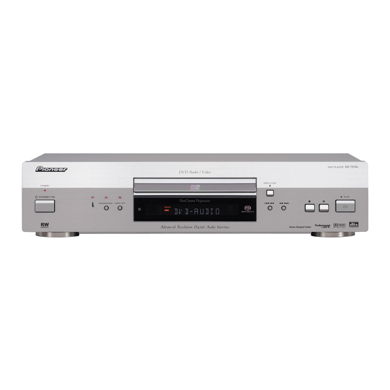
Page 154: Panel Facilities
8. PANEL FACILITIES DV-757Ai... - Page 155 [DV-757Ai/WYXJ] DV-757Ai...
- Page 156 [DV-S755Ai/RLXJ/NC] DV-757Ai...
- Page 157 DV-757Ai...
- Page 158 DV-757Ai...
- Page 159 DV-757Ai...