Philips CEM2000/00 Service Manual
Hide thumbs
Also See for CEM2000/00:
- User manual (26 pages) ,
- Quick start manual (1 page) ,
- Brochure (2 pages)
Table of Contents
Advertisement
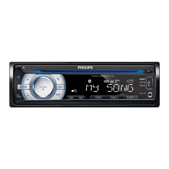
Car entertainment system
CONTENTS
Technical specification ..................................................................1-2
Service measurement setup..........................................................1-3
Service aids .................................................................................1-4
Instructions on CD playability ...............................................2-1.. 2-2
Block diagram ................................................................................3-1
Wiring diagram ..............................................................................4-1
Circuit diagram ..................................................................5-1..5-5
Layout diagram..................................................................5-6..5-7
Panel board
Circuit diagram .........................................................................6-1
Layout diagram..................................................................6-2..6-3
Circuit diagram..........................................................................7-1
Layout diagram ..................................................................7-2..7-3
Exploded view diagram .................................................................8-1
Revision list ...................................................................................9-1
©
Copyright 2010 Philips Consumer Electronics B.V. Eindhoven, The Netherlands
All rights reserved. No part of this publication may be reproduced, stored in a retrieval
system or transmitted, in any form or by any means, electronic, mechanical, photocopying,
or otherwise without the prior permission of Philips.
Published by LX 1046 Service Audio
Version 1.1
Subject to modification
CEM2000
/00/55/51
CEM2000X
3141 785 35131
/78
Advertisement
Table of Contents

Related Manuals for Philips CEM2000/00


Summary of Contents for Philips CEM2000/00
-
Page 1: Table Of Contents
Revision list ...................9-1 © Copyright 2010 Philips Consumer Electronics B.V. Eindhoven, The Netherlands All rights reserved. No part of this publication may be reproduced, stored in a retrieval system or transmitted, in any form or by any means, electronic, mechanical, photocopying, or otherwise without the prior permission of Philips. -
Page 2: Technical Specification
1 - 2 TECHNICAL SPECIFICATION Power supply 12 V DC (11 V - 16 Frequency range 87.5 - 108.0 MHz (100kHz General inforamtion Radio V), negative ground - FM per step in auto search and 50kHz per step in manual Fuse 15 A search) - Page 3 MEASUREMENT SETUP Tuner FM Bandpass LF Voltmeter 250Hz-15kHz e.g. PM2534 e.g. 7122 707 48001 RF Generator e.g. PM5326 S/N and distortion meter e.g. Sound Technology ST1700B Use a bandpass filter to eliminate hum (50Hz, 100Hz) and disturbance from the pilottone (19kHz, 38kHz). Tuner AM (MW,LW) Bandpass LF Voltmeter...
-
Page 4: Service Aids
SERVICE AIDS WARNING All ICs and many other semi-conductors are susceptible to electrostatic discharges (ESD). Careless handling during repair can reduce life drastically. When repairing, make sure that you are connected with the same potential as the mass of the set via a wrist wrap with resistance. Keep components and tools also at this potential. -
Page 5: Instructions On Cd Playability
2 - 1 INSTRUCTIONS ON CD PLAYABILITY Customer complaint "CD related problem" Set remains closed! check playability playability ok ? For flap loaders (= access to CD drive possible) "fast" lens cleaning cleaning method is recommended check playability playability ok ? Play a CD for at least 10 minutes check playability... - Page 6 2 - 2 INSTRUCTIONS ON CD PLAYABILITY PLAYABILITY CHECK LIQUID LENS CLEANING Before touching the lens it is advised to clean the surface of the lens by blowing clean air over it. For sets which are compatible with CD-RW discs This to avoid that little particles make scratches on use CD-RW Printed Audio Disc ....7104 099 96611 the lens.
-
Page 7: Block Diagram
3 - 1 3 - 1 SET BLOCK DIAGRAM... -
Page 8: Wiring Diagram
Wiring diagram 1117-ADJ 8M FLASH S5L8030 SERVO Board SA5888 MOTOR DRIVOE 4x16M SDRAM 4558 1117-3.3V 20Pin FFC LINE OUT ISO ANT AMP TDA7388 RADIO TDA7703 +5V IC 4558 7809 VOL IC 7313 20Pin FFC Main Board MCU 22Pin Connector TO PANEL Reset sw... - Page 9 5 - 1 5 - 1 CIRCUIT DIAGRAM - MAIN BOARD MCU PART...
- Page 10 5 - 2 5 - 2 CIRCUIT DIAGRAM - MAIN BOARD Power PART...
- Page 11 5 - 3 5 - 3 CIRCUIT DIAGRAM - MAIN BOARD Radio PART...
- Page 12 5 - 4 5 - 4 CIRCUIT DIAGRAM - MAIN BOARD Audio PART 1...
- Page 13 5 - 5 5 - 5 CIRCUIT DIAGRAM - MAIN BOARD Audio PART 2...
- Page 14 5 - 6 5 - 6 LAYOUT DIAGARM - MAIN BOARD TOP SIDE VIEW...
- Page 15 5 - 7 5 - 7 LAYOUT DIAGARM - MAIN BOARD BOTTOM SIDE VIEW...
- Page 16 6 - 1 6 - 1 CIRCUIT DIAGARM - PANEL BOARD RED+8V CEM2000-LCD R963 NC BLUE+8V LCD1 RED+8V R964 Q901 BLUE+8V R935 LED7 LED9 LED11 LED6 LED3 Q903 LED13 LED15 R938 R939 R958 RED+8V BLUE+8V R937 C901 Q904 680P R965 Q902 LED8 LED10...
- Page 17 6 - 2 6 - 2 LAYOUT DIAGRAM - PANEL BOARD...
- Page 18 7 - 1 7 - 1 CIRCUIT DIAGRAM - SERVO BOARD...
- Page 19 7 - 2 7 - 2 LAYOUT DIAGRAM - SERVO BOARD TOP SIDE VIEW...
- Page 20 7 - 3 7 - 3 LAYOUT DIAGRAM - SERVO BOARD BOTTOM SIDE VIEW...
-
Page 21: Exploded View Diagram
8 - 1 8 - 1 EXPLODED VIEW DIAGRAM 6501 6505 CD01 ASS02 6503 6502 6504 ASS05 PL01... -
Page 22: Revision List
9 - 1 Revision list Version1.0 ( 3141 785 35130) *Initial Release Version1.1 ( 3141 785 35131) *New version 51 added. - Page 23 Product Model CEM2000 Tate 2011-11-19 failure failure cause remark phenomena a. To check whether it is connect well of the ISO connector (4 PIN power input ). Whether it is loose of the 15A fuse of the ISO connector, or insert non in place. b.
- Page 24 failure failure cause remark phenomena a. To check whether the signal format of the disc is correspond to the request of the unit, whether there is any contamination or damage or light leakage on the surface of the disc. b. To check whether there is any abnormal of the rotation of the deck mechanism, or whether the disc is enter in position.
- Page 25 ANGUS ELECTRONICS CO., LTD Tel: (852) 2345 0540 Fax: (852) 2345 9948 Web Site: www.angus.com.hk PT7313E Stereo Audio Processor for Car Audio Princeton Technology Corp DESCRIPTION FEATURES The PT7313E is an audio processor designed for • 3 stereo inputs with gain selection, range from 0dB versatile application, including 3 stereo input selectors to +11.25dB in 3.75dB/step with adjustable gain, master volume control with low...
- Page 26 ANGUS ELECTRONICS CO., LTD Tel: (852) 2345 0540 Fax: (852) 2345 9948 Web Site: www.angus.com.hk PT7313E Princeton Technology Corp BLOCK DIAGRAM Speaker Attenuator With Mute RROUT LROUT RFOUT LFOUT TREB_R TREB_L TREBLE TREBLE BIN_L BIN_R BASS Master BASS BOUT_R BOUT_L Volume Loud LOUD_R...
- Page 27 ANGUS ELECTRONICS CO., LTD Tel: (852) 2345 0540 Fax: (852) 2345 9948 Web Site: www.angus.com.hk PT7313E Princeton Technology Corp ORDER INFORMATION Valid Part Number Package Type Top Code PT7313E-S 28 Pins, SOP, 300mil PT7313E PIN CONFIGURATION AGND DGND LFOUT TREB_L TREB_R RFOUT LROUT...
- Page 28 ANGUS ELECTRONICS CO., LTD Tel: (852) 2345 0540 Fax: (852) 2345 9948 Web Site: www.angus.com.hk PT7313E Princeton Technology Corp PIN DESCRIPTION Pin Name Description Pin No. Analog reference voltage (1/2VDD) Supply input voltage AGND Analog ground TREB_L Left channel input for treble controller TREB_R Right channel input for treble controller Right channel volume controller input...
- Page 29 ANGUS ELECTRONICS CO., LTD Tel: (852) 2345 0540 Fax: (852) 2345 9948 Web Site: www.angus.com.hk PT7313E Princeton Technology Corp CONTROL BUS SPECIFICATION BUS INTERFACE All functions of the PT7313E are controlled by the I C interface, the interface is consisting by SDA and SCL pins. Detail protocol of the I C bus will discuss on the next section.
- Page 30 ANGUS ELECTRONICS CO., LTD Tel: (852) 2345 0540 Fax: (852) 2345 9948 Web Site: www.angus.com.hk PT7313E Princeton Technology Corp ACKNOWLEDGE During the Acknowledge clock pulse (ACK), the SDA output port of the master device (μP) would be sets on Hi-Z state, if peripheral device (ex : audio processor) recognize the I C command the SDA line will be pull-down by slave device during the SCL clock pulse held in HIGH state period.
-
Page 31: Data Rate
ANGUS ELECTRONICS CO., LTD Tel: (852) 2345 0540 Fax: (852) 2345 9948 Web Site: www.angus.com.hk PT7313E Princeton Technology Corp DATA BYTES Function Master Volume Speaker ATT LR Speaker ATT RR Speaker ATT LF Speaker ATT RF Input Switch and Gain Bass Control Treble Control DATA RATE... -
Page 32: Function Description
ANGUS ELECTRONICS CO., LTD Tel: (852) 2345 0540 Fax: (852) 2345 9948 Web Site: www.angus.com.hk PT7313E Princeton Technology Corp FUNCTION DESCRIPTION MASTER VOLUME The table below gives a detailed description of the Master Volume Data Bytes. For example, a volume of -37.5dB is given by 0 0 0 1 1 1 1 0. - Page 33 ANGUS ELECTRONICS CO., LTD Tel: (852) 2345 0540 Fax: (852) 2345 9948 Web Site: www.angus.com.hk PT7313E Princeton Technology Corp INPUT SELECTOR The PT7313E provides 3 stereo input selector and following table shows the definition of the correspond register. The LD register is determinate the loudness function is ON or OFF, and G0 and G1 determinate the input gain of the selector output, this function is use to matching level of different sources to avoid overall volume difference.
- Page 34 ANGUS ELECTRONICS CO., LTD Tel: (852) 2345 0540 Fax: (852) 2345 9948 Web Site: www.angus.com.hk PT7313E Princeton Technology Corp TUNNING TONE CURVE CHARACTERISTICS The tone control response character is possible tuned to match user’s wishes, please refer to following chart to realize the characteristics between the different component values.
- Page 35 ANGUS ELECTRONICS CO., LTD Tel: (852) 2345 0540 Fax: (852) 2345 9948 Web Site: www.angus.com.hk PT7313E Princeton Technology Corp ABSOLUTE MAXIMUM RATINGS Parameter Symbol Min. Max. Unit Operating supply voltage Latch up current -100 +100 Human body model ESD grade Machine model -0.2 +0.2...
- Page 36 ANGUS ELECTRONICS CO., LTD Tel: (852) 2345 0540 Fax: (852) 2345 9948 Web Site: www.angus.com.hk PT7313E Princeton Technology Corp ELECTRICAL CHARACTERISTICS Unless otherwise specified: Ta=25℃, VDD=9V, RL=100KΩ, Rg=20Ω, all controls flat, F=1KHz, and all of peripheral components according to standard application circuit. Parameter Symbol Test Condition...
- Page 37 ANGUS ELECTRONICS CO., LTD Tel: (852) 2345 0540 Fax: (852) 2345 9948 Web Site: www.angus.com.hk PT7313E Princeton Technology Corp 50 100 200 50 100 200 Bass Response Treble Response Cref=22µF -100 -110 -100 -120 -130 -120 50 100 200 500 1k 5k 10k 50 100 200 500 1k...
- Page 38 ANGUS ELECTRONICS CO., LTD Tel: (852) 2345 0540 Fax: (852) 2345 9948 Web Site: www.angus.com.hk PT7313E Princeton Technology Corp Supply Voltage (V) Supply Voltage (V) Maximum Output Level (RL=100KΩ) Supply Current VS VDD Maximum output voltage 80KHz LPF 20-20KHz A-weighted Load (Kohm) Supply Voltage (V) Maximum Output Level VS R...
- Page 39 ANGUS ELECTRONICS CO., LTD Tel: (852) 2345 0540 Fax: (852) 2345 9948 Web Site: www.angus.com.hk PT7313E Princeton Technology Corp PACKAGE INFORMATION 28-PIN, SOP, 300MIL Symbol Min. Nom. Max. 2.65 0.10 0.30 0.31 0.51 0.20 0.33 17.90 BSC 10.30 BSC 7.50 BSC 1.27 BSC 0.38 1.27...
- Page 40 ANGUS ELECTRONICS CO., LTD Tel: (852) 2345 0540 Fax: (852) 2345 9948 Web Site: www.angus.com.hk PT7313E Princeton Technology Corp IMPORTANT NOTICE Princeton Technology Corporation (PTC) reserves the right to make corrections, modifications, enhancements, improvements, and other changes to its products and to discontinue any product without notice at any time. PTC cannot assume responsibility for use of any circuitry other than circuitry entirely embodied in a PTC product.
- Page 41 TDA7388 4 X 41W QUAD BRIDGE CAR RADIO AMPLIFIER FEATURES Figure 1. Package HIGH OUTPUT POWER CAPABILITY: ■ 4 x 41W/4Ω MAX. ■ 4 x 25W/4Ω @ 14.4V, 1KHz, 10% ■ Flexiwatt25 LOW DISTORTION ■ LOW OUTPUT NOISE ■ Table 1. Order Codes ST-BY FUNCTION ■...
- Page 42 TDA7388 Table 2. Absolute Maximum Ratings Symbol Parameter Value Unit Operating Supply Voltage DC Supply Voltage CC (DC) Peak Supply Voltage (t = 50ms) CC (pk) Output Peak Current: Repetitive (Duty Cycle 10% at f = 10Hz) Non Repetitive (t = 100µs) Power dissipation, (T = 70°C) case...
- Page 43 TDA7388 Table 4. Electrical Characteristcs (V = 14.4V; f = 1KHz; R = 600Ω; R = 4Ω;T = 25°C; Refer to the Test and application diagram, unless otherwise specified.) Symbol Parameter Test Condition Min. Typ. Max. Unit = ∞ Quiescent Current Output Offset Voltage Play Mode ±80...
- Page 44 TDA7388 Figure 4. Standard Test and Application Circuit 0.1µF 2200µF Vcc1-2 Vcc3-4 ST-BY OUT1 1µF MUTE 1µF OUT2 0.1µF C2 0.1µF OUT3 C3 0.1µF OUT4 C4 0.1µF S-GND D95AU335B 0.47µF 47µF 4/10...
- Page 45 TDA7388 P.C.B. AND COMPONENT LAYOUT OF THE FIGURE 4 Figure 5. Components & Top Copper Layer Figure 6. Bottom Copper Layer 5/10...
- Page 46 TDA7388 Figure 7. Quiescent Current vs. Supply Voltage Figure 10. Distortion vs. Output Power Figure 8. Quiescent Output Voltage Supply Figure 11. Distortion vs. Frequency Voltage Figure 12. Supply Voltage Rejection vs. Figure 9. Output Power vs. Supply Voltage Frequency. 6/10...
- Page 47 TDA7388 Figure 13. Output Noise vs. Source Figure 14. Power Dissipation & Efficiency vs. Resistance. Output Power. APPLICATION HINTS (ref. to the circuit of fig. 4) 5.1 SVR Besides its contribution to the ripple rejection, the SVR capacitor governs the turn ON/OFF time sequence and, consequently, plays an essential role in the pop optimization during ON/OFF transients.
- Page 48 TDA7388 Figure 15. Flexiwatt 25 Mechanical Data & Package Dimensions inch DIM. MIN. TYP. MAX. MIN. TYP. MAX. OUTLINE AND 4.45 4.50 4.65 0.175 0.177 0.183 1.80 1.90 2.00 0.070 0.074 0.079 MECHANICAL DATA 1.40 0.055 0.75 0.90 1.05 0.029 0.035 0.041 0.37...
- Page 49 TDA7388 REVISION HISTORY Table 5. Revision History Date Revision Description of Changes July 2005 First Issue 9/10...
- Page 50 TDA7388 Information furnished is believed to be accurate and reliable. However, STMicroelectronics assumes no responsibility for the consequences of use of such information nor for any infringement of patents or other rights of third parties which may result from its use. No license is granted by implication or otherwise under any patent or patent rights of STMicroelectronics.
- Page 51 TDA7703/TDA7703R Highly Integrated Tuner for AM/FM-Carradio TARGET DESIGN SPECIFICATION MAIN FEATURES FULLY INTEGRATED VCO FOR WORLD TUNING HIGH PERFORMANCE PLL FOR FAST RDS SYSTEM AM/FM MIXERS WITH HIGH IMAGE REJECTION LQFP44 INTEGRATED AM-LNA AND AM-PINDIODE AUTOMATIC SELF ALIGNMENT FOR IMAGE REJECTION INTEGRATED IF-FILTERS WITH HIGH SELECTIVITY, DYNAMIC RANGE AND ADAPTIVE BANDWIDTH CONTROL DIGITAL IF SIGNAL PROCESSING WITH HIGH PERFORMANCE AND FREE OF...
- Page 52 decoder with group block 1.0 DESCRIPTION synchronization. TDA7703/TDA7703R, a.k.a. HIT44, belong to the HIT (Highly Integrated Tuner) The utilization of digital signal processing family, a new generation of high performance results in numerous advantages against tuners for carradio applications. today’s tuners: •...
- Page 53 TDA7703/TDA7703R 3.0 PINOUT Figure 2 4.0 PIN ASSIGNMENT Pin No. Pin Name Description PLL loopfilter output TCAGCFM FM AGC time constant FMMIXDEC FM mixer decoupling FMIXIN FM mixer input GND-RF RF Ground FMPINDRV FM AGC PIN diode driver VCC-RF 5V supply for RF section TCAM AM AGC time constant PINDDEC...
- Page 54 TDA7703/TDA7703R AMMIXIN AM mixer input VREF165 1.65V reference voltage decoupling VREFDEC 3.3V reference voltage decoupling GND-DIG Digital GND VCC-DIG 5V supply for digital logic VCCREG1V2 VCC of 1.2V regulator REG1V2 1.2V regulator output VDD-3V3 3.3V VDD output / decoupling C bus data C bus clock VDD-1V2 1.2V DSP supply...
- Page 55 TDA7703/TDA7703R 5.0 FUNCTION DESCRIPTION 5.1 FM-Mixer The IMR mixer is optimized for optimum performance in case of a passive tuned prestage and for a passive fixed bandpass without tuning for low-cost application. The input frequency is downconverted to low IF with high image rejection. 5.2 FM - AGC The programmable RFAGC senses the mixer input, the IFAGC senses the IFADC input to avoid overload.
- Page 56 TDA7703/TDA7703R 5.12 I C ADDRESS SELECTION / RDS INTERRUPT INTERFACE PIN As explained also in 5.13.1, there is one pin (RDSINT, pin 29) dedicated to selecting the I address of the device. In the TDA7703R only this pin serves the additional function of RDS interrupt output to communicate to the uP when a new RDS block is available.
- Page 57 TDA7703/TDA7703R a chip address byte must be sent at the beginning of the transmission. The value can be C2 or C8 (according to the mode chosen at start-up during boot) for “write”; as many data bytes as one wants can follow the address before the communication is terminated. See the next section for details on the frame format;...
- Page 58 TDA7703/TDA7703R 6.0 ELECTRICAL CHARACTERISTICS 6.1 ABSOLUTE MAXIMUM RATINGS Limits Symbol Parameter Test Condition, Comments Units Abs. Supply Voltage Storage Temperature °C 6.2 THERMAL DATA Symbol Parameter Test Condition, Comments Value Units LQFP44 10x10, double-layer Thermal Resistance LQFP44 10x10, single-layer Thermal Resistance 6.3 GENERAL KEY PARAMETERS Limits Symbol...
- Page 59 TDA7703/TDA7703R 6.4 FM - SECTION VCC = 4.7V to 5.25V; Tamb = 27°C; f = 76 to 108 MHz; 60dBμV antenna level; mono signal, unless otherwise specified. Antenna level equivalence: 0dBμV = 1μV ref. deviation = 40 kHz rms, table to be inserted > <...
- Page 60 TDA7703/TDA7703R and 39 must be kept in order to latch the correct boot mode (serial bus configuration) Rev. 1.0 10/22...
- Page 61 TDA7703/TDA7703R 6.12.1 I C interface The following parameters apply to the serial bus communication when I C protocol has been selected at start-up. For the other electrical characteristics of the pins, section 6.9 applies. The parameters of the following table are defined as in Figure 1. Limits Symbol Parameter...
- Page 62 TDA7703/TDA7703R 7.0 Overall system performance 7.1 FM overall system performance Antenna level equivalence: 0dBμV = 1μV (Antenna terminal voltage with 50Ω source); no antenna dummy Reference deviation = 40 kHz, de-emphasis = 50 us, f = 1 KHz, V = 60 dBu audio Unless otherwise specified.
- Page 63 TDA7703/TDA7703R 7.2 AM MW overall system performance Antenna level equivalence: 0dBμV = 1μV Level referred to SG output before antenna dummy; capacitive dummy 15pF+65pF Reference modulation = 30%, f =400Hz, F =999kHz (1000 kHz for US), V = 74 dBu audio Unless otherwise specified Limits...
- Page 64 TDA7703/TDA7703R 7.3 AM LW overall system performance Antenna level equivalence: 0dBμV = 1μV before antenna dummy; capacitive dummy 15pF+65pF Reference modulation = 30%, f =400Hz, F =216kHz, V = 74 dBu audio Unless otherwise specified Limits Symbol Parameter Test Condition, Comments Units Tuning range LW (can be modified by the user)
- Page 65 TDA7703/TDA7703R 8.0 FRONT-END PROCESSING All the parameters in this section refer to the programmability of the FE part of the device (registers). The part of the registers that are not described here have either fixed values (shown in the tables with a black background) or values written by the tuner drivers, and therefore not directly by the user (shown in the tables with a red background, if the registers are written exclusively by the tuner drivers, and with orange background if they can be written by the user for the manual FE alignment operation).
- Page 66 TDA7703/TDA7703R 9.0 WEAK SIGNAL PROCESSING All the parameters in this section refer to the programmability of the DSP part of the device. The typical values are those set by default parameters (start-up without parametric change from main uP); the max and the min values refer to the programmability range. The values are referred to the typical application.
- Page 67 TDA7703/TDA7703R 9.1.3 Stereo blend (continuous set) Range Symbol Parameter Test Condition, Comments Units field strength = 80 dBu, pilot MaxSep Maximum stereo separation deviation = 6.75 kHz separation = MaxSep - 1 dB SBFSsp Start point vs. field strength no multipath present separation = 1 dB SBFSep End point vs.
- Page 68 TDA7703/TDA7703R 9.1.4 High cut control (continuous set) Range Symbol Parameter Test Condition, Comments Units minimum RF level for widest HCFSsp Start point vs. field strength HC filter (filter # 7) no multipath present maximum RF level for HCFSep End point vs. field strength narrowest HC filter (filter # 0) no multipath present Field strength-related...
- Page 69 TDA7703/TDA7703R 9.2 AM IF-processing 9.1.1 Channel selection filter Range Symbol Parameter Test Condition, Comments Units CSF BW Channel selection filter BW response: - 3dB ±3.7 9.2.1 Soft mute (continuous set) Range Symbol Parameter Test Condition, Comments Units audio atten = 1 dB SMsp Start point vs.
- Page 70 TDA7703/TDA7703R 10.0 APPLICATION SCHEMATIC Figure 5 (FM Eu/US/JP, AM LW/MW application) Rev. 1.0 20/22...
- Page 71 TDA7703/TDA7703R 11 PACKAGE INFORMATION Rev. 1.0 21/22...
- Page 72 TDA7703/TDA7703R Information furnished is believed to be accurate and reliable. However, STMicroelectronics assumes no responsibility for the consequences of use of such information nor for any infringement of patents or other rights of third parties which may result from its use. No license is granted by implication or otherwise under any patent or patent rights of STMicroelectronics. Specifications mentioned in this publication are subject to change without notice.