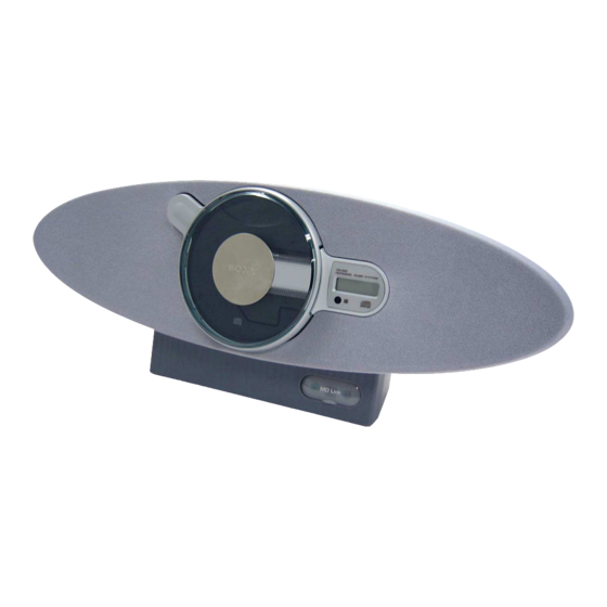
Sony ZS-D10 Service Manual
Personal audio system
Hide thumbs
Also See for ZS-D10:
- Operating instructions (2 pages) ,
- Specifications (2 pages) ,
- Operating instructions (2 pages)
Table of Contents
Advertisement
SERVICE MANUAL
Ver 1.0 2003.03
AUDIO POWER SPECIFICATIONS
(US model)
POWER OUTPUT AND TOTAL
HARMONIC DISTORTION
With 6-ohm loads, both channels driven
from 1 000 - 10 000 Hz; rated 3.5 W per
channel-minimum RMS power, with no
more than 10 % total harmonic distortion
in AC operation.
Other specifications
CD player section
System
Compact disc digital audio system
Laser diode properties
Material: GaAlAs
Wave length: 780 nm
Emission duration: Continuous
Laser output: Less than 44.6 µW
(This output is the value measured at a distance
of about 200 mm from the objective lens surface
on the optical pick-up block with 7 mm
aperture.)
Spindle speed
200 r/min (rpm) to 500 r/min (rpm)
(CLV)
Number of channels
2
Frequency response
20 - 20 000 Hz +1/–2 dB
Wow and flutter
Below measurable limit
Sony Corporation
9-877-106-01
2003C0500-1
Personal Audio Company
C 2003.03
Published by Sony Engineering Corporation
Model Name Using Similar Mechanism
CD Mechanism Type
Optical Pick-up Name
SPECIFICATIONS
Radio section
Frequency range
FM: 87.5 - 108 MHz
US, CND models:
AM: 530
- 1 710 kHz
AEP, UK, IT, EE models:
MW: 531 - 1611 kHz (9 kHz step)
530 - 1610 kHz (10 kHz step)
LW: 153 - 279 kHz
Antennas
FM: Telescopic antenna
AM/MW/LW: Built-in ferrite bar antenna
General
Speaker
Full range: 8 cm (3
1
⁄
in.) dia., 6 Ω, cone type
4
(2)
Input
LINE IN jack (stereo minijack):
Minimum input level 330 mV
Outputs
Headphones jack (stereo minijack):
For 16 - 68 Ω impedance headphones
OPTICAL DIGITAL OUT (CD) (optical output
connector):
Wavelength 630 - 690 nm
Power
output (US, CND models)
4
W + 4 W (at 6 Ω, 10% harmonic
distortion)
Maximum power output (AEP, UK, IT, EE models)
11 W
ZS-D10
Canadian Model
Power requirements
For Personal Audio System:
DC IN 10V jack accepts: Supplied AC power
adaptor for use with: 120V AC, 60 Hz (US, CND models)
230 V AC 50 Hz (AEP, UK, IT, EE, models)
For
remote control:
3 V DC, 2 size AAA (R03) batteries
Dimensions
Approx. 530 × 195 × 127 mm (w/h/d)
7
3
(20
⁄
× 7
⁄
× 5 inches) (incl. projecting parts)
8
4
Mass
Approx. 2.5 kg (5 lb. 8 oz)
Supplied accessory
AC power adaptor (1)
Remote control (1)
Design
and specifications are subject to change
without notice.
• Abbreviation
CND: Canadian model
EE : East European model
IT
: Italian model
PERSONAL AUDIO SYSTEM
US Model
AEP Model
UK Model
ZS-X3CP
KSM-900AAA
KSS-900A
Advertisement
Table of Contents

Related Manuals for Sony ZS-D10


Summary of Contents for Sony ZS-D10
-
Page 1: Specifications
Maximum power output (AEP, UK, IT, EE models) 20 - 20 000 Hz +1/–2 dB 11 W Wow and flutter Below measurable limit PERSONAL AUDIO SYSTEM Sony Corporation 9-877-106-01 2003C0500-1 Personal Audio Company C 2003.03 Published by Sony Engineering Corporation... -
Page 2: Leakage Test
OPERATION. REPLACE THESE COMPONENTS WITH DE FONCTIONNEMENT. NE REMPLACER CES COM- SONY PARTS WHOSE PART NUMBERS APPEAR AS POSANTS QUE PAR DES PIÈCES SONY DONT LES SHOWN IN THIS MANUAL OR IN SUPPLEMENTS PUB- NUMÉROS SONT DONNÉS DANS CE MANUEL OU LISHED BY SONY. -
Page 3: Table Of Contents
ZS-D10 SECTION 1 SERVICING NOTES TABLE OF CONTENTS SERVICING NOTES ..........NOTES ON HANDLING THE OPTICAL PICK-UP BLOCK OR BASE UNIT GENERAL ..............The laser diode in the optical pick-up block may suffer electro- static break-down because of the potential difference generated DISASSEMBLY by the charged electrostatic load, etc. -
Page 4: General
ZS-D10 SECTION 2 This section is extracted from GENERAL instruction manual. Location of controls Remote Control RADIO POWER BAND (US, CND models) MEMORY POWER AUTO PRESET OPERATE ., > (US, CND models) DISPLAY (AEP, UK, IT, EE models) PRESET –, + TUNE –, +... -
Page 5: Disassembly
ZS-D10 SECTION 3 DISASSEMBLY • This set can be disassembled in the order shown below. 3-1. DISASSEMBLY FLOW Note 1: The process described in can be performed in any order. Note 2: Without completing the process described in , the next process can not be performed. -
Page 6: Net Sub Assy
ZS-D10 Note: Follow the disassembly procedure in the numerical order given. 3-2. NET SUB ASSY 3 claw 5 net sub assy 2 claw 4 claw 4 claw 3 claw 2 claw 1 two screws (BVTP3 × 12) 3-3. COVER (CD) ASSY 1 five screws (BVTP3 ×... -
Page 7: Lcd Assy
ZS-D10 3-4. LCD ASSY 1 three screws (BVTP2.6 × 8) 3 FFC (24P) CN893 4 LCD assy 3-5. OPTICAL BLOCK (KSM-900AAA), RELAY BOARD 6 relay board 3 FFC (20P) (CNP704) 1 three screws (BVTP2.6 × 8) 7 insulator 4 OP flexible board... -
Page 8: Optical Pick-Up (Kss-900A)
ZS-D10 3-6. OPTICAL PICK-UP (KSS-900A) 4 screw (B1.7 × 4) 5 rack spring (780C) 8 optical pick-up (KSS-900A) 7 sled screw assy (780E) 1 screw (2 × 8) 2 holder (780C) 3 gear (B) (780C) 3-7. CABINET (REAR) ASSY 3 Stick a flat head driver... -
Page 9: Speaker (8Cm) (Lch/Rch)
ZS-D10 3-8. SPEAKER (8 cm) (Lch/Rch) Note: The speaker (8cm) (R ch) can be removed 4 four screws without removing the speaker (R ch) (8cm) in advance. (BVTP2.6 × 8) 5 speaker (8cm) (Lch) 9 speaker (8cm) (Lch) 8 four screws (BVTP2.6 ×... -
Page 10: Tuner Board
ZS-D10 3-9. TUNER BOARD 3 tuner board 2 three screws (BVTP2.6 × 8) 1 connector (CNP1) 3-10. CHASSIS SECTION MAIN board 4 chassis section 1 three connectors (CNP301, CNP303, CNP304) 2 two connectors (CNP391, CNP394) 3 three screws (BVTP3 × 10) -
Page 11: Door Sw Board, Main Board
ZS-D10 3-11. DOOR SW BOARD, MAIN BOARD 2 LED board 3 connector (CNP401) 7 door SW board 1 screw (BVTP2.6 × 8) 6 screw (BVTP2.6 × 8) 0 main board 5 shield plate 9 FFC (14P) (CNP805) 6 three screws (BVTP2.6 ×... -
Page 12: Assembly
ZS-D10 SECTION 4 ASSEMBLY • This set can be assembled in the order shown below. 4-1. ASSEMBLY FLOW 4-2. CD LID ASSY, SPRING (T) (Page 13) 4-3. COVER (CD) SUB ASSY, SPRING (U) AND COLLAR (Page 13) 4-4. HOW TO INSTALL THE CD LID ASSY (Page 14) 4-5. -
Page 13: Cd Lid Assy, Spring (T)
ZS-D10 Note: Follow the assembly procedure in the numerical order given. 4-2. CD LID ASSY, SPRING (T) portion ditch 1 Align portion of the spring (T) with the ditch of the CD lid assy and install the spring. CD lid assy 4-3. -
Page 14: How To Install The Cd Lid Assy
ZS-D10 4-4. HOW TO INSTALL THE CD LID ASSY 1 Push the collar fully in the direction of arrow A . 2 Align portion of the spring (T) which has been installed to the CD lid assy with the ditch of the collar and assemble them. -
Page 15: Gear
ZS-D10 4-5. GEAR 3 screw (BVTP2.6 × 8) cover (CD) sub assy ditch of CD lid assy 2 Align convex part of the the gear with the ditch of the CD lid assy and install the gear. 1 Lid the cover (CD) sub assy with the CD lid assy. -
Page 16: Electrical Adjustments
ZS-D10 SECTION 5 ELECTRICAL ADJUSTMENTS PRECAUTION AM (MW/LW) IF ADJUSTMENT 1. Setting Adjust for a maximum reading on level meter MEGA BASS : OFF 450 kHz TUNER SECTION 0 dB=1 µV AM VCO VOLTAGE ADJUSTMENT (US, CND) Adjustment Part Frequency Display Reading on Digital Voltmeter [AM (MW/LW) ] 1.0 ±... -
Page 17: Cd Section
ZS-D10 FOCUS BIAS CHECK Adjustment and Connecting Location: CD SECTION Procedure: – TUNER BOARD (Component Side) (US, CND) – Perform all CD section check in the test mode. 1. Connect the oscilloscope to TP (RF) and TP (VREF) on the CD board. -
Page 18: Diagrams
ZS-D10 SECTION 6 DIAGRAMS 6-1. BLOCK DIAGRAM – CD Section – RF AMP, FOCUS/TRACKING SERVO, DIGITAL SIGNAL PROCESSOR, CLV SERVO, DIGITAL FILTER, D/A CONVERTER FIN2 IC701 DETECTOR INTERPOLATION CD L-OUT LCHO ERROR EFMIN MUTE SLISE LEVEL 1 BIT FIN1 CORRECTION... -
Page 19: Block Diagram - Tuner Section
ZS-D10 6-2. BLOCK DIAGRAM – TUNER Section – FM IFT FM/AM RF AMP, MIX, OSC, FM/AM IF AMP, DET, MPX FM IF ANT1 (US, CND) (AEP, UK, IT, EE) FM TELESCOPIC ANTENNA L-OUT TU-LOUT IF-IN RF-IN MIX-OUT FM IF -OUT... -
Page 20: Block Diagram - Main Section
ZS-D10 6-3. BLOCK DIAGRAM – MAIN Section – POWER AMP L-OUT (Page 18) IC171 INPUT L-OUT SEL1 VIN1 OUT1 POWER VOLUME SURROUND TONE (Page 19) SELECT SP191 CONTROL CONTROL CONTROL SWITCH (L-CH) MUTING INPUT SELECT SWITCH, LOGIC R-CH SP291 Q171... -
Page 21: Note For Printed Wiring Boards And Schematic Diagrams
ZS-D10 6-4. NOTE FOR PRINTED WIRING BOARDS AND SCHEMATIC DIAGRAMS • Circuit Boards Location Note on Printed Wiring Boards: Note on Schematic Diagram: CONTROL (POWER) board • X : parts extracted from the component side. • All capacitors are in µF unless otherwise noted. pF: µµF •... -
Page 22: Printed Wiring Boards - Cd Section
ZS-D10 6-5. PRINTED WIRING BOARDS – CD Section – • See page 21 for Circuit Boards Location. :Uses unleaded solder. RELAY BOARD CD BOARD Q701 R707 CNP704 C701 C702 R729 R728 R710 R709 JC704 R726 JW729 R732 JW753 JC703 R730... -
Page 23: Schematic Diagram - Cd Section
ZS-D10 6-6. SCHEMATIC DIAGRAM – CD Section – • • See page 33 for Waveforms. See page 34 for IC Block Diagrams. CNP706 CNP704 M701 (SLED) S701 (LIMIT) ON:WHEN THE OPTICAL PICK-UP IS INNER POSITION M702 (SPINDLE) CNP705 C726 1000p... - Page 24 ZS-D10 6-7. PRINTED WIRING BOARD – TUNER Section (US, Canadian Models) – • See page 21 for Circuit Boards Location. • Semiconductor Location Ref. No. Location TUNER BOARD AM FERRITE-ROD ANTENNA ANT1 FM TELESCOPIC ANTENNA (VT) (ANT) (GND) (SHIELD CASE)
-
Page 25: Tuner Section (Us, Canadian Models)
ZS-D10 6-8. SCHEMATIC DIAGRAM – TUNER Section (US, Canadian Models) – • • See page 33 for Waveform. See page 34 for IC Block Diagrams. AM FERRITE-ROD KV1520NT 220p AM OSC ANTENNA 100p JC12 JC11 0.01 220k (VT) 1000p 0.01 100k 0.01... -
Page 26: Printed Wiring Board - Tuner Section (Aep, Uk, Italian, East European Models)
ZS-D10 6-9. PRINTED WIRING BOARD – TUNER Section (AEP, UK, Italian, East European Models) – • See page 21 for Circuit Boards Location. • Semiconductor Location Ref. No. Location TUNER BOARD L3-1 L3-2 MW FERRITE-ROD LW FERRITE-ROD ANTENNA ANTENNA ANT1... -
Page 27: Schematic Diagram - Tuner Section (Aep, Uk, Italian, East European Models)
ZS-D10 6-10. SCHEMATIC DIAGRAM – TUNER Section (AEP, UK, Italian, East European Models) – • • See page 33 for Waveform. See page 34 for IC Block Diagrams. KV1520NT-2 220p MW/LW OSC L3-1 100p MW FERRITE-ROD (VT) ANTENNA 220p 100p... -
Page 28: Schematic Diagram - Control/Panel Section
ZS-D10 6-11. SCHEMATIC DIAGRAM – CONTROL/PANEL Section – • See page 33 for Waveforms. LCD891 LIQUID CRYSTAL DISPLAY REMOTE CONTROL RECEIVER IC891 S401 IC RPM7140-H4 D891 ∗ R897 (ILLUMINATION) (WHITE:US) C891 FEY3864X (WHITE:US) 0.022 (EXCEPT WHITE:US) R401 SLR343BBT (EXCEPT WHITE:US) -
Page 29: Schematic Diagram - Audio/Power Supply Section
ZS-D10 6-12. SCHEMATIC DIAGRAM – AUDIO/POWER SUPPLY Section – • See page 34 for IC Block Diagrams. (2/2) (US,CND) R398 R399 Q391 4.7k 2.2k 2SC4178 L391 L391 WAVE D272 R397 SHAPER C278 1SS133T 4.7k (AEP,UK,IT,EE) D271 C277 R283 1SS133T 0.022... -
Page 30: Printed Wiring Board - Main Section
ZS-D10 6-13. PRINTED WIRING BOARD – MAIN Section – • :Uses unleaded solder. See page 21 for Circuit Boards Location. (US, CND) (AEP, UK, IT, EE) (Page 22) (Page 32) (Page 32) TUNER BOARD TUNER BOARD POWER AMP POWER AMP... -
Page 31: Printed Wiring Boards - Panel Section
ZS-D10 6-14. PRINTED WIRING BOARDS – PANEL Section – • :Uses unleaded solder. See page 21 for Circuit Boards Location. LCD BOARD CONTROL (PLAY) BOARD KH404 KH402 S403 S401 S412 S413 RADIO − TONE R414 PRESET − PRESET + BAND... -
Page 32: Printed Wiring Boards - Audio/Power Supply Section
ZS-D10 6-15. PRINTED WIRING BOARDS – AUDIO/POWER SUPPLY Section – • See page 21 for Circuit Boards Location. :Uses unleaded solder. • Semiconductor Location Ref. No. Location D171 POWER AMP BOARD D172 D271 D272 D901 IC171 IC271 IC171 IC271 C352... - Page 33 ZS-D10 • Waveforms – CD Board – – TUNER Board – – MAIN Board – 1 IC701 4 (RF) (CD play mode) qa IC2 w; (XOUT) wa IC801 ua (XT2) 1.4 Vp-p 2.6 Vp-p 1.3 Vp-p 13.3 µ s 30.5 µ s...
- Page 34 ZS-D10 • IC Block Diagrams – CD Board – IC701 LC78646E-E 78 77 76 75 74 73 72 71 69 68 67 66 65 64 63 62 61 FIN1 – FIN2 – TIN1 TBAL – – TIN2 – – TBAL –...
- Page 35 ZS-D10 IC702 BA5826FP-E2 SP– D.BUFF SL– D.BUFF LEVEL D.BUFF SHIFT D.BUFF SPIN LEVEL SHIFT SLIN THERMAL SHUT-DOWN MONITOR (SLIN) REG–B VREF REGO MUTE (FIN) DRIVER MUTE (TIN) LEVEL LEVEL SHIFT D.BUFF SHIFT D.BUFF F– T– D.BUFF D.BUFF OPOUT OPIN – TUNER Board –...
-
Page 36: Main Board
ZS-D10 IC2 LC72137M-TLM XOUT REFERENCE DIVIDER AOUT PHASE 12BITS DETECTOR PROGRAMMABLE CHARGE DIVIDER PUMP UNLOCK DETECTOR POWER ON RESET SWALLOW COUNTER FMIN 1/16,1/17 4BITS UNIVERSAL COUNTER AMIN IFIN – MAIN Board – IC321 BD3870FS-E2... -
Page 37: Ic Pin Function Description
ZS-D10 6-16. IC PIN FUNCTION DESCRIPTION • MAIN BOARD IC801 µPD789477GC-A31-8BT (SYSTEM CONTROLLER) Pin No. Pin Name Description 1, 2 — Not used 3 to 5 VLC2 to VLC0 — Terminal for doubler circuit capacitor connection to develop liquid crystal display drive voltage... - Page 38 ZS-D10 Pin No. Pin Name Description — Ground terminal Main system clock input terminal (4.19 MHz) Main system clock output terminal (4.19 MHz) System reset signal input from the reset signal generator “L”: reset For several hundreds msec. after the power supply rises, “L” is input, then it changes to “H”...
-
Page 39: Exploded Views
ZS-D10 SECTION 7 EXPLODED VIEWS NOTE: • -XX and -X mean standardized parts, so they • Items marked “*” are not stocked since they The components identified by mark 0 or dotted line with mark 0 are may have some difference from the original are seldom required for routine service. -
Page 40: Cover (Cd) Section
ZS-D10 7-2. COVER (CD) SECTION cabinet (rear) section cabinet (front) section-1 not supplied not supplied Ref. No. Part No. Description Remark Ref. No. Part No. Description Remark 3-250-645-01 PLATE (R), ORNAMENTAL (SILVER) 3-250-671-01 SPRING (T) 3-250-645-11 PLATE (R), ORNAMENTAL (WHITE) -
Page 41: Cabinet (Rear) Section
ZS-D10 7-3. CABINET (REAR) SECTION ANT1 cabinet (front) section-1 Ref. No. Part No. Description Remark Ref. No. Part No. Description Remark 4-951-620-31 SCREW (2.6), +BVTP 3-250-674-01 TERMINAL (ANT A) 4-951-620-01 SCREW (2.6X8), +BVTP 4-951-620-11 SCREW (2.6X10), +BVTP 3-250-640-01 CABINET (REAR) (AEP, UK, IT, EE) -
Page 42: Cabinet (Front) Section-1
ZS-D10 7-4. CABINET (FRONT) SECTION-1 cabinet (front) section-2 KSM-900AAA LCD891 LCD board Ref. No. Part No. Description Remark Ref. No. Part No. Description Remark 3-250-669-01 COVER (LCD) 4-975-762-11 INSULATOR 4-951-620-01 SCREW (2.6X8), +BVTP * 156 A-3663-874-A RELAY BOARD, COMPLETE LCD891 1-805-177-11 DISPLAY PANEL, LIQUID CRYSTAL... -
Page 43: Cabinet (Front) Section-2
ZS-D10 7-5. CABINET (FRONT) SECTION-2 cabinet (front) section-3 SP191 SP291 Ref. No. Part No. Description Remark Ref. No. Part No. Description Remark * 201 A-3663-972-A LED BOARD, COMPLETE (WHITE: US) * 203 A-3323-905-A TUNER BOARD, COMPLETE (AEP, UK, IT, EE) -
Page 44: Cabinet (Front) Section-3
ZS-D10 7-6. CABINET (FRONT) SECTION-3 not supplied not supplied not supplied not supplied F902 J391 cabinet (front) section-4 The components identified by Les composants identifiés par une mark 0 or dotted line with marque 0 sont critiques pour la mark 0 are critical for safety. -
Page 45: Cabinet (Front) Section-4
ZS-D10 7-7. CABINET (FRONT) SECTION-4 cabinet (front) section-5 Ref. No. Part No. Description Remark Ref. No. Part No. Description Remark * 301 A-3663-882-A DOOR SW BOARD, COMPLETE FFC (24P) * 306 A-3663-873-A CD BOARD, COMPLETE 4-951-620-01 SCREW (2.6X8), +BVTP * 303... -
Page 46: Cabinet (Front) Section-5
ZS-D10 7-8. CABINET (FRONT) SECTION-5 not supplied Ref. No. Part No. Description Remark Ref. No. Part No. Description Remark 3-250-639-01 CABINET (FRONT) (CND, AEP, UK, IT, EE) 3-250-649-01 LEVER 3-250-673-01 SPRING (B) 3-250-639-11 CABINET (FRONT) (SILVER) (US) 3-250-639-21 CABINET (FRONT) (WHITE) (US) 3-250-680-01 CHASSIS (LEVER) 4-951-620-01 SCREW (2.6X8), +BVTP... -
Page 47: Optical Pick-Up Section (Ksm-900Aaa)
ZS-D10 7-9. OPTICAL PICK-UP SECTION (KSM-900AAA) (including M701, M702) not supplied The components identified by Les composants identifiés par une mark 0 or dotted line with marque 0 sont critiques pour la mark 0 are critical for safety. sécurité. Replace only with part num- Ne les remplacer que par une pièce... -
Page 48: Electrical Parts List
ZS-D10 SECTION 8 ELECTRICAL PARTS LIST NOTE: • Due to standardization, replacements in the • Items marked “*” are not stocked since they The components identified by 0 or dotted line with mark mark parts list may be different from the parts speci- are seldom required for routine service. - Page 49 ZS-D10 CONTROL (PLAY) CONTROL (POWER) CONTROL (VOL) Ref. No. Part No. Description Remark Ref. No. Part No. Description Remark R713 1-216-809-11 METAL CHIP 1/10W < SWITCH > R714 1-216-853-11 METAL CHIP 470K 1/10W R715 1-216-849-11 METAL CHIP 220K 1/10W S401...
- Page 50 ZS-D10 DC JACK DOOR SW JACK Ref. No. Part No. Description Remark Ref. No. Part No. Description Remark A-3663-881-A DC JACK BOARD, COMPLETE < RESISTOR > ************************ 1-533-233-31 FUSE HOLDER R191 1-247-807-31 CARBON 1/4W R192 1-216-821-11 METAL CHIP 1/10W < CAPACITOR >...
- Page 51 ZS-D10 MAIN Ref. No. Part No. Description Remark Ref. No. Part No. Description Remark A-3663-876-A MAIN BOARD, COMPLETE (AEP, UK, IT, EE) C826 1-162-927-11 CERAMIC CHIP 100PF A-3663-893-A MAIN BOARD, COMPLETE (US, CND) C827 1-162-927-11 CERAMIC CHIP 100PF C828 1-162-927-11 CERAMIC CHIP...
- Page 52 ZS-D10 MAIN Ref. No. Part No. Description Remark Ref. No. Part No. Description Remark < TRANSISTOR > R809 1-216-821-11 METAL CHIP 1/10W R810 1-216-817-11 METAL CHIP 1/10W Q101 8-729-028-97 TRANSISTOR DTC114TUA-T106 R811 1-216-845-11 METAL CHIP 100K 1/10W Q201 8-729-028-97 TRANSISTOR...
- Page 53 ZS-D10 MAIN POWER AMP RELAY TUNER Ref. No. Part No. Description Remark Ref. No. Part No. Description Remark < VIBRATOR > < CABLE HOLDER > X801 1-781-775-21 VIBRATOR, CERAMIC (4.19MHz) * KH372 1-565-384-11 HOLDER, CABLE 3P X802 1-795-915-11 VIBRATOR, CRYSTAL (32.768kHz)
- Page 54 ZS-D10 TUNER Ref. No. Part No. Description Remark Ref. No. Part No. Description Remark 1-162-964-11 CERAMIC CHIP 0.001uF 1-161-051-00 CERAMIC 0.01uF 1-162-970-11 CERAMIC CHIP 0.01uF (US, CND) (AEP, UK, IT, EE) 1-161-772-11 CERAMIC 0.1uF (AEP, UK, IT, EE) 1-162-970-11 CERAMIC CHIP 0.01uF...
- Page 55 ZS-D10 TUNER Ref. No. Part No. Description Remark Ref. No. Part No. Description Remark < DIODE > 1-216-853-11 METAL CHIP 470K 1/10W 8-719-078-48 DIODE KV1471ETR1-3 (AEP, UK, IT, EE) 8-719-078-48 DIODE KV1471ETR1-3 1-216-845-11 METAL CHIP 100K 1/10W 8-719-050-69 DIODE KV1520N...
- Page 56 ZS-D10 TUNER Ref. No. Part No. Description Remark Ref. No. Part No. Description Remark 1-216-821-11 METAL CHIP 1/10W < TRANSFORMER > 1-433-741-11 TRANSFORMER, IF 1-419-465-11 COIL (DET) < VIBRATOR > 1-795-449-11 VIBRATOR, CRYSTAL (75MHz) ************************************************************** MISCELLANEOUS ************** FFC (24P) FFC (14P)
- Page 57 ZS-D10 MEMO...
-
Page 58: Revision History
ZS-D10 REVISION HISTORY Clicking the version allows you to jump to the revised page. Also, clicking the version at the upper right on the revised page allows you to jump to the next revised page. Ver. Date Description of Revision...