Sony XVM-R70 Service Manual
Hide thumbs
Also See for XVM-R70:
- Operating instructions manual (65 pages) ,
- Product manual (3 pages) ,
- User manual (3 pages)
Table of Contents
Advertisement
Quick Links
Download this manual
See also:
Owner's Manual
SERVICE MANUAL
Ver. 1.2 2005.07
•
This set consists of the following units.
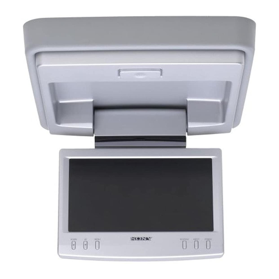
MONITOR
XVM-R70
CONNECTION BOX
XA-115
REMOTE COMMANDER
RM-X122
Monitor XVM-R70
System
Liquid crystal color display
Display
Manual flipdown panel
Drive system
TFT-LCD active matrix system
Picture size
7 inches wide screen (16:9)
154 × 87 mm, 176 mm
(6
× 3
in., 7 in.) (w/h, d)
1/8
1/2
Picture segment
336,960 (w 1440 × h 234) dots
Power requirements
12 V DC car battery (negative ground)
Current drain
Approx. 800 mA
Dimensions
230 × 57 × 270 mm
(9
× 2
× 10
in.) (w/h/d)
1/8
3/8
3/4
Operating temperature
5 °C – 45 °C (41 °F – 113 °F)
Mass
Approx. 1.5 kg (3 lb 5 oz)
Connection box XA-115
A/V Output
Output Impedance: less than 220 Ω
less than 100 pF
Output Level:
0 dBs ±0.3 dB (0.775 V rms)
(Vol Max)
Video:
75 Ω 1Vp-p
A/V Input × 3
Input Impedance:
more than 10 KΩ
less than 1000 pF
Input Level:
±1.3 dBs +0/–0.3 dB (0.775 V rms)
Video:
75 Ω 1 Vp-p
DC output
7.5 V (max 2 A)
Dimensions
150 × 42 × 80 mm
(6 × 1
× 3
in.) (w/h/d)
11/16
1/4
Mass
Approx. 260 g (9 oz)
Sony Corporation
9-961-143-03
2005G04-1
e Vehicle Group
© 2005.07
Published by Sony Engineering Corporation
XVM-R70
SPECIFICATIONS
Card remote commander RM-X122
Power requirements
CR2025 lithium battery
Operable range
Approx. 2.5 m (8.22 ft.)
Dimensions
52 × 125 × 10 mm
(2
1/8
(w/h/d)
Mass
Approx. 40 g (1 oz)
(including batteries)
Supplied accessories
Connection box XA-115 (1)
Card remote commander RM-X122
(with supplied battery) (1)
Monitor cable (5 m) (1)
Power supply cord (1)
DC-DC cord (3 m) (1)
Stereo Mini Plug-to-Plug cable (5 m) (1)
Mounting plate (1)
Screws (4)
Tapping Screws (4)
Operating Instructions (1)
Design and specifications are subject to change
without notice.
US Model
Canadian Model
AEP Model
UK Model
× 5 ×
in.)
13/32
OVERHEAD MONITOR
E Model
1
Advertisement
Table of Contents

Related Manuals for Sony XVM-R70


Summary of Contents for Sony XVM-R70
-
Page 1: Overhead Monitor
7.5 V (max 2 A) Dimensions 150 × 42 × 80 mm (6 × 1 × 3 in.) (w/h/d) 11/16 Mass Approx. 260 g (9 oz) OVERHEAD MONITOR Sony Corporation 9-961-143-03 2005G04-1 e Vehicle Group © 2005.07 Published by Sony Engineering Corporation... -
Page 2: Table Of Contents
CRITIQUES POUR LA SÉCURITÉ DE FONCTIONNEMENT. NE REPLACE THESE COMPONENTS WITH SONY PARTS WHOSE REMPLACER CES COMPOSANTS QUE PAR DES PIÈCES SONY PART NUMBERS APPEAR AS SHOWN IN THIS MANUAL OR DONT LES NUMÉROS SONT DONNÉS DANS CE MANUEL OU IN SUPPLEMENTS PUBLISHED BY SONY. -
Page 3: Servicing Notes
XVM-R70 Ver 1.1 SECTION 1 SERVICING NOTES NOTE FOR REPLACEMENT OF THE EEP ROM (IC402) The EEP ROM (IC402) contains all data by which the LCD screen is defined. When the EEP ROM is replaced, the normal LCD screen will not appear. -
Page 4: General
XVM-R70 SECTION 2 GENERAL This section is extracted from instruction manual. Location of controls Monitor 1 OPEN button 4 MENU button Press to open the monitor. Press to adjust the various display 2 Receptor for the card remote settings. 5 REVERSE button*... - Page 5 AUDIO SUBTITLE For the monitor operations: For DVD operations: 1 ATT button When a Sony mobile DVD player is connected to this unit, you can control Press to quickly attenuate the the basic functions with the card remote volume. commander.
-
Page 6: Connection Diagram
(IR) Output* DVD (MV) connector is only for MV-101. For details, refer to the Installation/Connections * “PS one” is a trademark of Sony Computer Entertainment Inc. manual supplied with MV-101. (AEP, UK model) Not used in this unit (US, Canadian, E model) -
Page 7: Disassembly
XVM-R70 SECTION 3 DISASSEMBLY Note : This set can be disassemble according to the following sequence. 3-1. SKIRT (BASE) (Page 8) 3-2. BASE BOARD (Page 8) 3-3. SW BOARD 3-4. COVERS (HINGE) (Page 9) (Page 9) 3-5. LCD BLOCK ASSY (Page 10) 3-6. -
Page 8: Skirt (Base)
XVM-R70 Note : Follow the disassembly procedure in the numerical order given. 3-1. SKIRT (BASE) qa insulating sheet (base) 0 base plate 9 screw BTP 2.6 x 8 6 two screws BTP 2.6 x 8 5 skirt (base) 1 two screws... -
Page 9: Sw Board
XVM-R70 3-3. SW BOARD 1 two screws B 2.6 x 6 2 SW board 3-4. COVERS (HINGE) two claws 5 cover (hinge front) 3 cover (hinge rear) 1 two screws BTP 2.6 x 8... -
Page 10: Lcd Block Assy
XVM-R70 3-5. LCD BLOCK ASSY 3 LCD block assy 2 two screws PS 3 x 10 1 two screws PS 3 x 10 3-6. CASE (LCD REAR) 1 four claws 3 window (IR) 2 four claws 7 claw 6 claw... -
Page 11: Chassis (Lcd)
XVM-R70 3-7. CHASSIS (LCD) 5 two screws 6 screw P 2 x 5 P 2 x 5 7 screw P 2 x 5 8 two screws P 2 x 5 4 two screws P 2 x 5 qf chassis (LCD) -
Page 12: Lcd Board
XVM-R70 3-8. LCD BOARD 3 screw B 2 x 6 9 two t screws P 2 x 8 4 lug 5 retainer (LCD) qa LCD board 0 two screws P 2 x 8 2 CN850 6 screw (+ B 2 x 6... -
Page 13: Test Mode
XVM-R70 Ver 1.1 SECTION 4 TEST MODE Setting Method: 1. Place the POWER SELECT switch on the set into the B posi- tion. 2. Turn power on. While holding the RESET key down, depress key. Then release the RESET key and the key in this order. -
Page 14: Electrical Adjustments
XVM-R70 SECTION 5 ELECTRICAL ADJUSTMENTS 5-1. EQUIPMENT USED The following measuring equipment are used for these electrical adjustments: • Oscilloscope • NTSC pattern generator • Stabilized power supply • Digital voltmeter • Frequency counter 5-2. CONNECTION OF EQUIPMENT Unless otherwise specified, the equipment should be connected as shown below. -
Page 15: Dc-Dc Converter Adjustment
XVM-R70 5-4. DC-DC CONVERTER ADJUSTMENT 5-6. INVERTER HIGH VOLTAGE CHECK Condition: DIMMER switch OFF 5-4-1. Frequency Adjustment Adjustment Method: 5-6-1. Voltage Check 1) Connect frequency counter between TP801 (+) and TP803 (–). Checking Method: 2) Adjust RV801 so that the reading on the counter stands at the 1) Connect oscilloscope between TP853 (+) and TP854 (–) using... -
Page 16: Com Voltage/Position Adjustment
XVM-R70 5-11. V COM VOLTAGE/POSITION ADJUSTMENT 5-12-3. White Limiter Level Adjustment Adjustment Method: Condition: TEST MODE (See 13 page) 1) Select White Limit from the FOR FACTORY MODE. 2) Connect oscilloscope between TP811 (+) and TP500 (–). 1. Voltage Setup Adjustment... -
Page 17: R Sub Contrast Adjustment
XVM-R70 5-12-6. R Sub Contrast Adjustment 5-12-9. γ 2 Adjustment Adjustment Method: Adjustment Method: 1) Select R SUB CONT from the FOR FACTORY MODE. 1) Select Gamma2 from the FOR FACTORY MODE. 2) Connect oscilloscope between TP812 (+) and TP500 (–). - Page 18 XVM-R70 Adjustment Location: – LCD BOARD – (SIDE A) RV351 CN850 TP352 TP353 RV350 TP803 IC350 TP853 TP854 TP804 RV801 TP807 TP805 TP806 CN800 TP350 IC601 TP354 TP809 6-pin T850 RV802 TP612 RV601 TP600 T800 CN902 CN403 CN401 RV600 TP507...
-
Page 19: Diagrams
XVM-R70 SECTION 6 DIAGRAMS 6-1. IC PIN DESCRIPTION • IC400 µPD780022AY-N14-9ET (SYSTEM CONTROL) Pin No. Pin Name Pin Description Test mode setting input PW-ON Power ON control signal output — Not used (Open) — Not used (Open) — Not used (Open) - Page 20 XVM-R70 Pin No. Pin Name Pin Description — Not used (Open) A MUTE Audio muting signal output LCD up/down reverse control signal output LCD left/right reverse control signal output TFT ON LCD ON/OFF control signal output SIDE3 Display size 3 control signal output...
-
Page 21: Block Diagram -Video Section
XVM-R70 6-2. BLOCK DIAGRAM — VIDEO SECTION — VD PULSE SHAPE Q500 IC500 RGB DECODER VD IN HD OUT (Page 22) SYNC CSYNCIN SYNC VD OUT KILL COUNT Q501,502 CN950 C IN CVBS BPF/ R-Y/B-Y BRIGHT/ INVERT (Page 22) MATRIX... -
Page 22: Block Diagram -Display Section
XVM-R70 6-3. BLOCK DIAGRAM — DISPLAY SECTION — IC501 RGB BLANKING RV601 IC601 BIAS (Page 21) Q600,D601 RV600 Q506 PLL FREERUN IC600 DISPLAY CONTROL OSCI PDOS CPH1 STH1 STH2 HD OUT HDIR LCD1 MASK (Page 21) COUNT LIQUID CRYSTAL DISPLAY PANEL... - Page 23 • B : B– Line. • H : adjustment for repair. 1V/DIV 50µsec/DIV 0.5V/DIV 20µsec/DIV 0.2V/DIV 200nsec/DIV • CN401 of XVM-R70 is connected to Connection Box with a monitor cable. 3.5Vp-p 2.2Vp-p 0.8Vp-p Power voltage is dc 14.4 V from ACC cord of the Connec- tion Box and fed with regulated dc power supply.
-
Page 24: Printed Wiring Board -Lcd Section (1/2)
XVM-R70 6-4. PRINTED WIRING BOARD — LCD SECTION (1/2) — • Refer to page 23 for Common Note on Printed Wiring Boards. • Semiconductor Location Ref. No. Location D356 D501 G-10 R415 D602 D-12 R416 Q402 D603 D-12 D604 D-12... -
Page 25: Printed Wiring Board -Lcd Section (2/2)
XVM-R70 6-5. PRINTED WIRING BOARD — LCD SECTION (2/2) — • Refer to page 23 for Common Note on Printed Wiring Boards. (Page 27) BASE BOARD CN953 • Semiconductor D350 D351 D352 IC404 BASE BOARD (Page 27) LCD1 Location CN952... -
Page 26: Printed Wiring Board -Base Section (1/2)
XVM-R70 6-6. PRINTED WIRING BOARD — BASE SECTION (1/2) — • Refer to page 23 for Common Note on Printed Wiring Boards. BASE BOARD (SIDE A) S951 (RESET) TP975 TP956 TP951 TP960 TP972 TP961 TP963 TP969 TP967 TP965 TP978 TP962... -
Page 27: Printed Wiring Board -Base Section (2/2)
XVM-R70 6-7. PRINTED WIRING BOARD — BASE SECTION (2/2) — • Refer to page 23 for Common Note on Printed Wiring Boards. SW BOARD (SIDE B) SW BOARD (SIDE A) • Semiconductor Location Ref. No. Location Ref. No. Location D901... -
Page 28: Schematic Diagram -Lcd Section (1/3)
XVM-R70 6-8. SCHEMATIC DIAGRAM — LCD SECTION (1/3) — • Refer to page 23 for Waveforms and Common Note on Schematic Diagram and page 31 for IC Block Diagrams. CN950 R977 CN954 R976 TP975 TP977 TP976 S951 TP978 R972 D901... -
Page 29: Schematic Diagram -Lcd Section (2/3)
XVM-R70 6-9. SCHEMATIC DIAGRAM — LCD SECTION (2/3) — • Refer to page 23 for Waveforms and Common Note on Schematic Diagram and page 31 for IC Block Diagrams. (Page 28) D410 L400 IC B/D D412 C423 C401 IC401 R445... -
Page 30: Schematic Diagram -Lcd Section (3/3)
XVM-R70 6-10. SCHEMATIC DIAGRAM — LCD SECTION (3/3) — • Refer to page 23 for Waveforms and Common Note on Schematic Diagram and page 32 for IC Block Diagrams. TP614 C606 C603 L600 C605 C604 C602 R659 IC B/D RV601... -
Page 31: Ic Block Diagrams
XVM-R70 6-11. IC BLOCK DIAGRAMS IC500 AN2546FH-AV LOGIC LOGIC LOGIC LOGIC PONRST IICBUS SYNCSEPA 32 HDOUT COMDC 31 VDOUT PHASE SECAM BLACK ADJ VSYNC 30 PWM OUT HHKILL DROP COMP CLAMP 29 VCC3 VCOM 28 VCOM OUT CTRAP OUT VERT. - Page 32 XVM-R70 IC401 µPD6467GR-546-E1 20 H SYNC 19 V SYNC DATA INPUT INSTRUCTION DECODER CONTROL SIGNALS SHIFT REGISTER DATA WRITE-IN CHARACTER SIZE H-ADDRESS DISPLAY ADDRESS VIDEO RAM REGISTER REGISTER CONTROL COUNTER REGISTER DATA BACK SELECT INTERRUPT V-SIZE H-POSITION H-ADDRESS DATA COUNTER...
- Page 33 XVM-R70 IC600 TC200G02AF-0104 43 42 41 40 MASK PDOS TSTB H-OUT STH1 H-COUNTER STH2 HDIR CHP2 CPH1 32 STV2 V-COUNTER 31 NGEO1 CPH3 30 NGEO2 29 NGEO3 SCKE 28 CPV V-OUT 27 CX FIELD DISCRI V-SEP 26 VDD INT/EXT SEL...
-
Page 34: Exploded Views
XVM-R70 SECTION 7 EXPLODED VIEWS NOTE: • The mechanical parts with no reference • Color Indication of Appearance Parts The components identified by mark 0 or dotted line with mark number in the exploded views are not supplied. Example : 0 are critical for safety. -
Page 35: Base (2) Section
XVM-R70 7-2. BASE (2) SECTION not supplied (SW board) not supplied not supplied not supplied not supplied supplied not supplied not supplied not supplied Ref. No. Part No. Description Remark Ref. No. Part No. Description Remark A-3274-916-A BASE BOARD, COMPLETE... -
Page 36: Lcd Section
3-254-862-11 BUTTON (FUNCTION) * LCD1 1-805-280-11 DISPLAY PANEL, LIQUID CRYSTAL (TFT) (7 in. WIDE) 3-254-860-01 CASE (LCD FRONT) 4-969-961-11 EMBLEM (NO.4), SONY 7-685-504-19 SCREW +B 2X6 TYPE2 N-S 3-254-863-01 WINDOW (IR) 7-621-255-35 SCREW +P 2X5 3-254-868-01 CUSHION (LCD) 7-621-773-95 SCREW +B 2.6X6... -
Page 37: Connection Box Section (Xa-115)
XVM-R70 7-4. CONNECTION BOX SECTION (XA-115) not supplied not supplied CN202 not supplied not supplied CN300 J200 J300 CN301 CN901 J201 CN201 CN200 J901 not supplied not supplied not supplied not supplied Ref. No. Part No. Description Remark Ref. No. -
Page 38: Electrical Parts List
XVM-R70 SECTION 8 BASE ELECTRICAL PARTS LIST NOTE: • Due to standardization, replacements in • Items marked “*” are not stocked since The components identified by mark 0 or dotted line with mark the parts list may be different from the they are seldom required for routine service. - Page 39 XVM-R70 Ref. No. Part No. Description Remark Ref. No. Part No. Description Remark A-3274-919-A LCD BOARD, COMPLETE C513 1-126-396-11 ELECT CHIP 47uF C514 1-104-915-11 TANTAL. CHIP 2.2uF ******************** C515 1-104-915-11 TANTAL. CHIP 2.2uF 1-827-343-11 CORD (WITH CONNECTOR) C516 1-162-970-11 CERAMIC CHIP 0.01uF...
- Page 40 XVM-R70 Ref. No. Part No. Description Remark Ref. No. Part No. Description Remark C626 1-125-891-11 CERAMIC CHIP 0.47uF * CN404 1-691-741-21 PIN, CONNECTOR (PC BOARD) 2P C627 1-162-970-11 CERAMIC CHIP 0.01uF CN800 1-794-237-21 CONNECTOR, FFC/FPC 30P C628 1-162-970-11 CERAMIC CHIP 0.01uF...
- Page 41 XVM-R70 Ref. No. Part No. Description Remark Ref. No. Part No. Description Remark IC403 8-759-698-19 IC XC61CN2702MR Q600 8-729-013-35 TRANSISTOR 2SC4118-OY-TE85L IC404 6-701-681-01 IC RPM7140-V4 (IR) Q601 8-729-905-35 TRANSISTOR 2SC4081-R IC500 6-704-269-01 IC AN2546FH-AV Q800 6-550-139-01 TRANSISTOR IMZ1A-T108 IC501 6-704-276-01 IC CD74HCT4053PWR...
- Page 42 XVM-R70 Ref. No. Part No. Description Remark Ref. No. Part No. Description Remark R434 1-216-817-11 METAL CHIP 1/10W R521 1-216-808-11 METAL CHIP 1/10W R435 1-216-821-11 METAL CHIP 1/10W R522 1-216-833-11 METAL CHIP 1/10W R436 1-216-826-11 METAL CHIP 2.7K 1/10W R523...
- Page 43 XVM-R70 Ref. No. Part No. Description Remark Ref. No. Part No. Description Remark R657 1-216-837-11 METAL CHIP 1/10W R880 1-216-839-11 METAL CHIP 1/10W R658 1-216-825-11 METAL CHIP 2.2K 1/10W R881 1-216-834-11 METAL CHIP 1/10W R659 1-216-821-11 METAL CHIP 1/10W R882...
- Page 44 XVM-R70 Ver 1.1 Ref. No. Part No. Description Remark ACCESSORIES ************ 1-478-042-11 REMOTE COMMANDER (RM-X122) 1-827-262-11 CORD, CONNECTION (MONITOR) (5m) 1-827-263-11 CORD, CONNECTION (POWER) (including F901,F902) 1-827-264-11 CORD, CONNECTION (STEREO MINI) (5m) 1-827-326-11 CORD, CONNECTION (DC-DC) (3m) 3-254-962-11 MANUAL, INSTRUCTION (ENGLISH,FRENCH)
- Page 45 XVM-R70 US Model Canadian Model SERVICE MANUAL AEP Model UK Model E Model Ver. 1.2 2005.07 SUPPLEMENT-1 File this supplement with the service manual. Subject : Change the LCD, BASE and SW boards. Printed wiring board and schematic diagram of new type, and changed parts list are described in this Supplement-1.
- Page 46 XVM-R70 TABLE OF CONTENTS 1. DIAGRAMS 1-1. Printed Wiring Board –LCD Section (1/2)– ....... 4 1-2. Printed Wiring Board –LCD Section (2/2)– ....... 5 1-3. Printed Wiring Board –Base Section (1/2)– ......6 1-4. Printed Wiring Board –Base Section (2/2)– ......7 1-5.
- Page 47 • B : B– Line. • H : adjustment for repair. 1V/DIV 50µsec/DIV 0.5V/DIV 20µsec/DIV 0.2V/DIV 200nsec/DIV • CN401 of XVM-R70 is connected to Connection Box with a monitor cable. 3.5Vp-p 2.2Vp-p 0.8Vp-p Power voltage is dc 14.4 V from ACC cord of the Connec- tion Box and fed with regulated dc power supply.
- Page 48 XVM-R70 1-1. PRINTED WIRING BOARD — LCD SECTION (1/2) — : Uses unleaded solder. • Semiconductor Location Ref. No. Location D356 D602 D-12 R415 D603 D-12 R416 Q402 D604 D-12 D804 LCD BOARD (SIDE B) Q401 D805 Q400 D852 D853...
- Page 49 XVM-R70 1-2. PRINTED WIRING BOARD — LCD SECTION (2/2) — : Uses unleaded solder. (Page 7) BASE BOARD CN953 • Semiconductor D350 D351 D352 IC404 BASE BOARD (Page 7) LCD1 Location CN952 LIQUID CRYSTAL DISPLAY PANEL (Page 7) Ref. No.
- Page 50 XVM-R70 1-3. PRINTED WIRING BOARD — BASE SECTION (1/2) — : Uses unleaded solder. BASE BOARD (SIDE A) S951 (RESET) TP975 TP956 TP951 TP960 TP972 TP961 TP963 TP969 TP967 TP965 TP978 TP962 TP964 TP970 TP968 TP971 TP959 TP979 TP973 TP976...
- Page 51 XVM-R70 1-4. PRINTED WIRING BOARD — BASE SECTION (2/2) — : Uses unleaded solder. SW BOARD (SIDE B) SW BOARD (SIDE A) • Semiconductor Location Ref. No. Location Ref. No. Location D901 D-12 Q951 D902 Q952 D903 Q954 S951 (DOOR)
- Page 52 XVM-R70 1-5. SCHEMATIC DIAGRAM — LCD SECTION (1/3) — • Refer to page 3 for Waveforms and page 11 for IC Block Diagrams. CN950 R977 CN954 R976 TP975 TP976 S951 TP977 TP978 D901 CN953 TP966 TP969 TP970 TP973 TP972 TP965...
- Page 53 XVM-R70 1-6. SCHEMATIC DIAGRAM — LCD SECTION (2/3) — • Refer to page 3 for Waveforms and page 11 for IC Block Diagrams. (Page 8) IC B/D D410 L400 C423 D412 C402 C401 IC401 R445 TP407 R440 C426 R451 R471...
- Page 54 XVM-R70 1-7. SCHEMATIC DIAGRAM — LCD SECTION (3/3) — • Refer to page 3 for Waveforms and page 12 for IC Block Diagrams. TP614 C606 C603 L600 C605 C604 C602 IC B/D R659 RV601 R638 R639 C626 IC B/D Q600...
- Page 55 XVM-R70 • IC BLOCK DIAGRAMS IC500 AN2546FH-AV LOGIC LOGIC LOGIC LOGIC PONRST IICBUS SYNCSEPA 32 HDOUT COMDC 31 VDOUT PHASE SECAM BLACK ADJ VSYNC 30 PWM OUT HHKILL DROP COMP CLAMP 29 VCC3 VCOM 28 VCOM OUT CTRAP OUT VERT.
- Page 56 XVM-R70 IC401 µPD6467GR-546-E1 20 H SYNC 19 V SYNC DATA INPUT INSTRUCTION DECODER CONTROL SIGNALS SHIFT REGISTER DATA WRITE-IN CHARACTER SIZE H-ADDRESS DISPLAY ADDRESS VIDEO RAM REGISTER REGISTER CONTROL COUNTER REGISTER DATA BACK SELECT INTERRUPT V-SIZE H-POSITION H-ADDRESS DATA COUNTER...
- Page 57 XVM-R70 IC600 TC200G02AF-0104 43 42 41 40 MASK PDOS TSTB H-OUT STH1 H-COUNTER STH2 HDIR CHP2 CPH1 32 STV2 V-COUNTER 31 NGEO1 CPH3 30 NGEO2 29 NGEO3 SCKE 28 CPV V-OUT 27 CX FIELD DISCRI V-SEP 26 VDD INT/EXT SEL...
- Page 58 XVM-R70 SECTION 2 BASE ELECTRICAL PARTS LIST NOTE: • Due to standardization, replacements in • Items marked “*” are not stocked since The components identified by mark 0 or dotted line with mark the parts list may be different from the they are seldom required for routine service.
- Page 59 XVM-R70 Ref. No. Part No. Description Remark Ref. No. Part No. Description Remark A-3274-919-A LCD BOARD, COMPLETE C513 1-126-396-11 ELECT CHIP 47uF C514 1-104-915-11 TANTAL. CHIP 2.2uF ******************** C515 1-104-915-11 TANTAL. CHIP 2.2uF 1-827-343-11 CORD (WITH CONNECTOR) C516 1-162-970-11 CERAMIC CHIP 0.01uF...
- Page 60 XVM-R70 Ref. No. Part No. Description Remark Ref. No. Part No. Description Remark C627 1-162-970-11 CERAMIC CHIP 0.01uF CN800 1-794-237-21 CONNECTOR, FFC/FPC 30P C628 1-162-970-11 CERAMIC CHIP 0.01uF CN850 1-815-494-21 PIN, CONNECTOR 2P C800 1-164-315-11 CERAMIC CHIP 470PF * CN902...
- Page 61 XVM-R70 Ref. No. Part No. Description Remark Ref. No. Part No. Description Remark IC403 8-759-698-19 IC XC61CN2702MR Q506 8-729-026-52 TRANSISTOR 2SA1576A-T106-R IC404 6-701-681-01 IC RPM7140-V4 (IR) Q600 8-729-013-35 TRANSISTOR 2SC4118-OY-TE85L IC500 6-704-269-01 IC AN2546FH-AV Q601 8-729-905-35 TRANSISTOR 2SC4081-R IC501 6-704-276-01 IC CD74HCT4053PWR...
- Page 62 XVM-R70 Ref. No. Part No. Description Remark Ref. No. Part No. Description Remark R433 1-216-816-11 METAL CHIP 1/10W R515 1-216-835-11 METAL CHIP 1/10W R434 1-216-817-11 METAL CHIP 1/10W R517 1-216-825-11 METAL CHIP 2.2K 1/10W R435 1-216-821-11 METAL CHIP 1/10W R518 1-216-829-11 METAL CHIP 4.7K...
- Page 63 XVM-R70 Ref. No. Part No. Description Remark Ref. No. Part No. Description Remark R645 1-216-835-11 METAL CHIP 1/10W R873 1-216-865-11 METAL CHIP 1/10W R646 1-216-843-11 METAL CHIP 1/10W R874 1-216-865-11 METAL CHIP 1/10W R647 1-216-857-11 METAL CHIP 1/10W R875 1-218-708-11 METAL CHIP 4.7K...
- Page 64 XVM-R70 REVISION HISTORY Clicking the version allows you to jump to the revised page. Also, clicking the version at the upper on the revised page allows you to jump to the next revised page. Ver. Date Description of Revision 2003.07 2003.10...