
Related Manuals for Sony BVP-550


Summary of Contents for Sony BVP-550
- Page 1 COLOR VIDEO CAMERA BVP-550 BVP-550P MAINTENANCE MANUAL 1st Edition Serial No. 10001 and Higher (BVP-550) Serial No. 40001 and Higher (BVP-550P)
- Page 2 ! WARNING This manual is intended for qualified service personnel only. To reduce the risk of electric shock, fire or injury, do not perform any servicing other than that contained in the operating instructions unless you are qualified to do so. Refer all servicing to qualified service personnel.
- Page 3 X-RAY RADIATION WARNING CAUTION Be sure that parts replacement in the high voltage block and adjustments made to the high voltage circuits are Danger of explosion if battery is incorrectly carried out precisely in accordance with the procedures replaced. given in this manual. Replace only with the same or equivalent type recommended by the manufacturer.
-
Page 5: Table Of Contents
MIC Connector..............2-8 (E) 2-7-3. TEST OUT/REMOTE Connector ........2-9 (E) 2-8. Disconnecting/Connecting of Flexible Card Wires ......2-10 (E) 2-9. Board Replacement ................2-11 (E) 2-9-1. MB-602 Board ..............2-11 (E) 2-9-2. CN-1120/1121 Board ............2-12 (E) 1 (E) BVP-550 BVP-550P... - Page 6 4-2-14. Detail Clip Adjustment ............4-17 (E) 4-2-15. Skin Tone Adjustment ............4-18 (E) 4-2-16. Zebra Adjustment ............... 4-19 (E) 4-2-17. Automatic Iris Adjustment ..........4-20 (E) 4-2-18. File Store ................4-20 (E) 4-2-19. Menu Setting After Adjustment .........4-20 (E) 2 (E) BVP-550 BVP-550P...
- Page 7 RIGHT PANEL AND PLUG-IN BOARDS ..........5-3 LEFT PANEL AND BOARDS ..............5-4 CHASSIS AND SHOLDER PAD ............5-5 BOTTOM BLOCK ................... 5-6 VIEW FINDER ..................5-7 TRIPAD ADAPTOR ................5-9 SCREWS AND WASHERS ..............5-10 3 (E) BVP-550 BVP-550P...
- Page 8 MB-602 BOARD ..................8-22 FRAME WIRING ..................8-24 9. Board Layouts VA-163 BOARD ..................9-1 AT-95 BOARD ................... 9-2 SG-234 BOARD ..................9-3 DA-88 BOARD ................... 9-4 IF-510 BOARD ................... 9-5 MB-602 BOARD ..................9-6 VF-60 BOARD ................... 9-7 4 (E) BVP-550 BVP-550P...
-
Page 9: Manual Structure
Manual Structure Purpose of this manual This manual is the maintenance manual for Color Video Camera BVP-550/550P. This manual describes the information items necessary when the unit is supplied and installed, items on maintenance, and items that premise the service based on the components parts such as alignment, schematic diagrams, board layouts and spare parts list, assuming use of system and service engineers. -
Page 10: Relative Manuals
This manual is necessary for application and operation of this unit. • System manual (Not supplied with this unit) This manual is necessary for connection and operation of this unit and other peripheral equipments. If this manual is required, please contact Sony service organization 6 (E) BVP-550 BVP-550P... -
Page 11: Installation
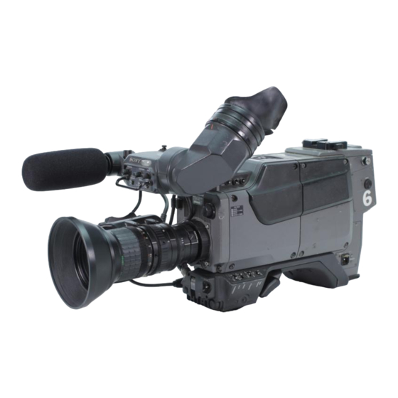
Section 1 Installation 1-1. Supplied Accessories Accessories Sony Part No. Qt’y Microphone 1-542-233-11 Microphone Spacer 3-179-882-01 Tripod Adaptor VCT-14 — Operation Manual — (English, German) each Maintenance Manual — 1-2. Connectors and Cables 1-2-1. Connector Input/Output Signals Output Signal • TEST OUT BNC 75 Ω... - Page 12 • In use of Color VF By controlling the voltage at pin 5 during operation, switching between the decoded return video signal and the camera component signal is done in the viewfinder. H: Camera, L: Return video 1-2 (E) BVP-550 BVP-550P...
- Page 13 5 Vp-p 5 Vp-p, 4700 Ω, Pull up IIC CLOCK OUT (CA) 5 Vp-p IIC DATA IN/OUT (CA) 5 Vp-p, 4700 Ω, Pull up IIC CLOCK OUT (ST) 5 Vp-p IIC DATA IN/OUT (ST) (0 dBu=0.775 Vrms) 1-3 (E) BVP-550 BVP-550P...
- Page 14 Note 4 : Specifications of TAPE REM Signal Tape Remaining (VTR) Input Signal at Pin 25 Remark TAPE1 TAPE2 +5 V +5 V +3.4 V +5 V +3.1 V G TALLY lamp lights at +3.1 V +5 V +2.2 V 1-4 (E) BVP-550 BVP-550P...
- Page 15 No connection No connection No connection No connection No connection No connection No connection No connection No connection No connection No connection 18 MHz OUT (G) GND for 18 MHz 18 MHz OUT (X) 3.3 Vp-p 1-5 (E) BVP-550 BVP-550P...
-
Page 16: Connection Connector
YES NO OFF ON OFF OFF YES YES YES OFF OFF YES YES YES OFF OFF ON OFF YES YES YES OFF ON OFF YES YES YES For details on the setup menu, refer to Section 3. 1-6 (E) BVP-550 BVP-550P... - Page 17 GEN: Reference signal for external synchronization which : PHANTOM POWER switch is input at GENLOCK IN connector of CA Turn on when connecting the PHANTOM +48 V micro- Factory-set position: RET phone to MIC connector. Factory-set position: ON 1-7 (E) BVP-550 BVP-550P...
-
Page 18: Instance Of Sytem Configuration
COAX CABLE ENG/EFP LENS OTHER OPTIONAL ACCESSORIES For BVP-500/500P STANDALONE UNIT BKP-5910/5910P SCRIPT HOLDER BKP-7911/7912 For BVP-550/550P ELECTRET CONDENSER MICROPHONE ECM-MS5 MICROPHONE C-74 (Sony P/N 1-542-099-11) CRADLE SUSPENSION CRS-3P CARRYING CASE LC-303SFT For CA-550/550P TELEPROMPTER UNIT BKP-5971 1-8 (E) BVP-550 BVP-550P... - Page 19 MSU-700 CAMERA CONTROL UNIT CCU-700/700P CCA-5 CABLE (*1) *1: CCA-5 CABLE LENGTH RCP-700/701 CCA-5 CCA-5 CCA-5 Total length 200m or less *2: TRIAX CABLE LENGTH Diameter Maximum length 8.5 mm 1000 m 14.5 mm 2000 m 1-9 (E) BVP-550 BVP-550P...
- Page 20 1-5. Instance of Sytem Configuration COLOR VIDEO CAMERA BVP-550/550P 1.5" VF(BVF-10/10CE) CCD UNIT OHB-450/450P CAMERA ADAPTOR DIGITAL VIDEO CASSETTE OHB-451/451P CA-550/550P RECORDER OHB-550/550P DVW-250/250P OHB-550WS/550WSP CCZ CABLE ENG/EFP LENS REMOTE MASTER AC ADAPTOR CONTROL SETUP AC-550/550P PANEL UNIT RCP-700 MSU-700...
-
Page 21: Optional Accessories For Viewfinder
• Fog-proof Filter (Sony Part No. 1-547-341-11) Use in place of the MC protector shown in the figure. -
Page 23: Service Overview
2. Standardization of Parts itself. Some repair parts supplied by Sony differ from those used for the unit. These are because of parts common- 2-1-2. Note on Replacement of PR-211 Board ality and improvement. -
Page 24: Removal Of Cabinet
To remove the both side panels Loosen the four screws respectively. 2-3. Location of Printed Circuit Boards Viewfinder block Camera block VR-199 SW-732 LP-84 MB-602 CN-1120 PR-211 CN-1121 CN-1142 IF-510 DA-88 CN-1122 SG-234 AT-95 VA-163 SW-730 SW-731 SW-733 SW-742 2-2 (E) BVP-550 BVP-550P... -
Page 25: Circuit Description
OHB-450/451/550/550W series (available separately) is The DR-302 board consists of a motor-drive circuit, and a described here. The BVP-550/550P is called as BVP, and servo circuit comprised of a selected filter detection and OHB-450/451/550/550W series is called as OHB in this filter position voltage generation circuits. - Page 26 Signals from external equipment: Reference signal for external synchronization, Return video signal By combination with these signals, the IF-510 board outputs the following signals. • VBS OUT signal Output via a buffer amplifier to external equipment. 2-4 (E) BVP-550 BVP-550P...
- Page 27 V RESET/H CONT mode when the CCU is connected to the camera. Input channels of the V RESET and H CONT signals differ depending on the type of CA in connection with the camera. 2-5 (E) BVP-550 BVP-550P...
-
Page 28: Periodic Replacement Part
2-5. Periodic Replacement Part Parts listed below are periodic replacement parts. They are subject to cracks with the lapse of time. Check sometimes by visual, and replace as necessary. Description Sony P/N PAD ASSY (LARGE) A-8278-237-A PAD ASSY (SMALL) A-8278-238-A... -
Page 29: Cleaning
• To protect the viewfinder lens from drops, put the MC protector in the filter holder and attach the eyecup securely. Hold ring Align red lines VF tube sub MC protector assembly Filter holder Eyecup 2-7 (E) BVP-550 BVP-550P... -
Page 30: Replacement Of External Connectors
CCD Unit removal. PA-181 2-7-2. MIC Connector 1. Remove the two screws and remove the MIC connec- tor. Then unsolder it. DR-271 Precision P2.6 MIC connector 2. Install a new connector in the reverse procedures of removal. 2-8 (E) BVP-550 BVP-550P... -
Page 31: Test Out/Remote Connector
(Large). REMOTE connector. Connector bracket Pad assembly(small) Pad assembly(large) Precision P2.6 2. Remove the seven screws and remove the V shoe bracket. 4. Install a new connector in the reverse procedures of removal. V Shoe bracket 2-9 (E) BVP-550 BVP-550P... -
Page 32: Disconnecting/Connecting Of Flexible Card Wires
2. Slide portion B in the opposite direction of the arrow and lock each connector. 2-10 (E) BVP-550 BVP-550P... -
Page 33: Board Replacement
“2-8. Disconnecting/Connecting of Flexible Card Wires”. CN12 5. Remove the four screws and remove the four supports. Remove the MB-602 board. MB-602 CN13 CN14 CN32 Support 7. Install a new board in the reverse procedures of removal. Support CN-1142 PR-211 2-11 (E) BVP-550 BVP-550P... -
Page 34: Cn-1120/1121 Board
(Refer to “2-11. Replacement of DC/DC Convertor Unit”.) 4. Remove the rail(upper). 5. Remove the four screws and remove the rail bracket. CN-1120 Precision B2.6 CN-1121 B2.6 Rail bracket Rail(upper) 8. Install a new board in the reverse procedures of removal. 2-12 (E) BVP-550 BVP-550P... -
Page 35: Replacement Of Function Switches
Switch garud BTP2.6 Shielding plate Shielding plate BTP2.6 Drop protection cushion SW-730 SW-731 5. Install a new switch in the reverse procedures of P2.6 removal. P2.6 5. Install a new switch in the reverse procedures of removal. 2-13 (E) BVP-550 BVP-550P... -
Page 36: Vf Disp Switch
6. Remove the two screws and remove the SW-732 board and the drop protection cushion. Handle holder 7. Unsolder the terminals and remove the switch to be replaced. SW-732 Drop protection cushion B2.6 8. Install a new switch in the reverse procedures of removal. 2-14 (E) BVP-550 BVP-550P... -
Page 37: Replacement Of Dc/Dc Convertor Unit
DC convertor unit. shown in the figure. DC/DC Convertor Unit B2.6 5. Install a new DC/DC convertor unit pushing with hands. Secure it to the MB-602 board with the two screws that were removed in Step 2. 2-15 (E) BVP-550 BVP-550P... -
Page 38: Replacement Of Crt On Viewfinder
Anode cable CRT cable CN21 CN31 LP-85 9. Install a new CRT in the reverse procedures of remov- When installing the upper chassis, take care not to clamp the harness between upper and lower chassis. VF-60 2-16 (E) BVP-550 BVP-550P... -
Page 39: Setup Menu
OHB-450/550 series Camera Adaptor CA-550/550P Supply power from a camera control unit CCU-700/700P, AC adaptor AC-550/550CE or VTR. • Switches and Button DISP switch DISP MENU MENU SEL switch LEVEL CANCEL button < > FRONT VIEW CANCEL 3-1(E) BVP-550 BVP-550P... - Page 40 6. To exit from the setup menu, set the DISP switch to OFF. • ROM version Contents in the menu and factory settings may differ from the descriptions in this manual depending on the version of ROM on the AT-95 board. 3-2(E) BVP-550 BVP-550P...
-
Page 41: Operation Menu
-3,[0], 3, 6, 9, 12, Selects the gain value for each gain switch position 18, 24, 30 dB (LOW, MIDDLE, HIGH) -3, 0, 3, 6, [9], 12, 18, 24, 30dB HIGH -3, 0, 3, 6, 9, 12, [18], 24, 30dB 3-3(E) BVP-550 BVP-550P... - Page 42 Turns the skin tone detail function on and off. AUTO HUE Press MENU SEL Starts to automatically adjust the volume of effect of the skin detail auto DETECT switch to execute. hue function. (Does not function at present.) 3-4(E) BVP-550 BVP-550P...
- Page 43 The gamma and knee compensation values do not change with a lapse of time because of the digital-processing camera. Therefore, the LEVEL AUTO adjustment does not contain the gamma and knee adjustments unlike a conventional camera. 3-5(E) BVP-550 BVP-550P...
-
Page 44: Paint Menu
Press MENU SEL Sets all settings on the DETAIL2 page to 0. switch to execute. (When you press MENU SEL switch, the “CLEAR” indication flashes. Press MENU SEL switch again to execute; press CANCEL button to cancel.) 3-6(E) BVP-550 BVP-550P... - Page 45 Press MENU SEL Sets all settings on the KNEE/W.CLIP page to 0. switch to execute. (When you press MENU SEL switch, the “CLEAR” indication flashes. Press MENU SEL switch again to execute; press CANCEL button to cancel.) 3-7(E) BVP-550 BVP-550P...
- Page 46 Returns the current amount of paint adjustments and switch setting to their reference value stored as a reference file. When both USER and PRESET are set to ON, the matrix constant compensation is total value of the USER and PRESET matrix. 3-8(E) BVP-550 BVP-550P...
-
Page 47: Maintenance Menu
Press the MENU SEL switch again to execute; press CANCEL button to cancel.) When the master modulation shading is adjusted, the V. SAW component for the R and B V-modulation shadings of the prism is simultaneously compensated. 3-9(E) BVP-550 BVP-550P... - Page 48 Therefore, the LEVEL AUTO adjustment does not contain the gamma and knee adjustments unlike a conventional camera. Before first using the camera with the OHB-450/451/550/550WS (or their PAL version) installed, or After replacing the CCD unit, be sure to execute the automatic black shading adjustment. 3-10(E) BVP-550 BVP-550P...
-
Page 49: Reference Menu
Stores specific data for a CCD unit to be used as the OHB files. switch to execute. The standard values are stored at the factory. If the power is turned off without execution of the FILE STORE after clearing the file, the original setting is restored. 3-11(E) BVP-550 BVP-550P... -
Page 50: System Config Menu
Adjusts the R, G or B pre-knee 1 level on the VA board. (Continued) PREKNEE2 R/G/B XXX ([XX]) Adjusts the R, G or B pre-knee 2 level on the VA board. APERTURE XXX ([XX]) Adjusts the aperture compensation signal level. 3-12(E) BVP-550 BVP-550P... - Page 51 [ON], OFF VF ? DISPLAY Turns on and off the indication of ? mark at the top-right of the VF screen with the DISP switch set to ON when the self-diagnosis result is NG (no good)and so on. 3-13(E) BVP-550 BVP-550P...
-
Page 52: Self-Diagnosis
3-2. Self-Diagnosis 3-2. Self-Diagnosis The BVP-550/550P has a diagnosis mode used for self-diagnosis of every plug-in board and the OHB. The diagnosis page is displayed on the viewfinder screen. • Operation Select “Diagnosis” page of the Operation menu referring to Section 3-1. -
Page 53: Electrical Alignment
White Window Chart Extension board EX-464 (option) Make a square hole at the center Sony P/N: J-6395-040-A of a black sheet of paper. For BVP-550/550P plug-in boards VF extension harness Extension board BKP-7900 (option) Sony P/N: J-6395-050-A For CCU-700/700P plug-in boards... -
Page 54: Notes On Adjustment
PAGE : Skin Detail (P4) grayscale chart. (For more details, consult your Sony service represen 10. How to change the setting values tative.) To enter or cancel the setting value of items, which 7. -
Page 55: Initial Setting
The setup menus from the Operation menu to System MENU : Operation config menu are used in BVP-550/550P adjustment. PAGE : Gain Sw (?3) ITEM : Low → 0 dB Perform the following setting to display all of the setup ITEM : Middle →... -
Page 56: Adjustment For Installation Of Ohb
1. Set the menu as follows and adjust the frequency by turning the MENU SEL switch. MENU : System config PAGE : Y/Chroma (S2) ITEM : SC Freq Specifications: 3,579,545 ±10 Hz (for NTSC) 4,433,168 ±5 Hz (for PAL) 4-4 (E) BVP-550 BVP-550P... -
Page 57: Va Gain Adjustment
Set the menu as follows and adjust the level by turning the MENU SEL switch. MENU : Operation PAGE : Auto Setup (?8) ITEM : Test→2 Specifications: A = 100 ±2 IRE (for NTSC) A = 700 ±14 mV (for PAL) (Waveform Monitor) 4-5 (E) BVP-550 BVP-550P... -
Page 58: Black Shading Adjustment
C=MINIMUM • If the shading adjustment is not completed, perform the adjustment again referring to the message displayed on the viewfinder or MSU. If the re-adjustment still is not completed, consult Sony service representative. (Waveform Monitor) Preparations: Connect the waveform monitor to the TEST OUT connec- tor. - Page 59 : Black Shading (M3) ITEM : Black M 4. If the shading is monitored, makes the waveform flat referring to the following table. 5. Perform the adjustments for R-ch and B-ch following the same procedures as for G-ch. 4-7 (E) BVP-550 BVP-550P...
-
Page 60: White Shading Adjustment
Set the R/G/B switch (on the side panel) to G. 3. If the white shading is monitored, makes the waveform flat referring to the following tables. 4. Perform the adjustments for R-ch and B-ch following the same procedures as for G-ch. 4-8 (E) BVP-550 BVP-550P... - Page 61 Execute the Reference File Store. Press the MENU SEL switch (on the front panel). 6. After adjustments are completed, set the switch and menu as follows. ENC/RGB switch (on the side panel) → ENC Menu setting: 4-9 (E) BVP-550 BVP-550P...
-
Page 62: Master Black Adjustment
2. Set the menu as follows, and adjust the gamma correction for (M) by turning the MENU SEL switch. PAGE : Video Level (P1) ITEM : Gamma (M) Specifications: B = 60 ±2 IRE (for NTSC) B = 420 ±14 mV (for PAL) (Waveform Monitor) 4-10 (E) BVP-550 BVP-550P... -
Page 63: Flare Adjustment
7. Confirm that the carrier leakage does not observed at (Waveform Monitor) portion C on the waveform monitor. Specifications: C = Minimum (Waveform Monitor) 8. Set the menu as follows. MENU : Paint PAGE : Video Level (P1) ITEM : Test→Off 4-11 (E) BVP-550 BVP-550P... -
Page 64: Knee And White Clip Adjustment
Specifications: B = 109 ±2 IRE (for NTSC) (Waveform Monitor) B = 763 ±10 mV (for PAL) 8. Repeat the steps 6 and 7 alternately, until the carrier leakage is minimized. 9. WHITE BAL switch (on the side panel) → PRST 4-12 (E) BVP-550 BVP-550P... -
Page 65: Crispening Adjustment
Knee slope 109/763 107/750 107/750 107/750 the black level of the waveform is just decreased, or White clip 109/763 107/749 105/735 103/721 turn the MENU SEL switch so that the crispening level is an appropriate value. 4-13 (E) BVP-550 BVP-550P... -
Page 66: Level Dependent Adjustment
ITEM : Level Dep.→On Adjustment procedures: 1. Adjust the iris of the lens to satisfy the white level A. Specifications: A = 100 ±2 IRE (for NTSC) A = 700 ±14 mV (for PAL) (Waveform Monitor) 4-14 (E) BVP-550 BVP-550P... -
Page 67: Detail Frequency Adjustment
ITEM : Detail→On Adjustment procedures: 1. Adjust the iris control of the lens to satisfy the white level A. Specifications: A = 100 ±2 IRE (for NTSC) A = 700 ±14 mV (for PAL) (Waveform Monitor) 4-15 (E) BVP-550 BVP-550P... -
Page 68: H/V Ratio Adjustment
ITEM : Detail→On Adjustment procedures: 1. Adjust the iris control of the lens to satisfy the white level A. Specifications: A = 100 ±2 IRE (for NTSC) A = 700 ±14 mV (for PAL) (Waveform Monitor) 4-16 (E) BVP-550 BVP-550P... -
Page 69: Detail Level Adjustment
MENU SEL switch. MENU : Paint PAGE : Detail 1 (P2) ITEM : Level (Waveform Monitor) Adjust the detail signal level to be added to each step in the grayscale chart for the desired level. 4-17 (E) BVP-550 BVP-550P... -
Page 70: Skin Tone Adjustment
Specifications: Adjust the edges of portion (b) to Width the desired clip level. Saturation (Waveform Monitor) (Vector scope Monitor) 3. Set the menu as follows. MENU : Paint PAGE : Skin Detail (P4) ITEM : Gate→Off 4-18 (E) BVP-550 BVP-550P... -
Page 71: Zebra Adjustment
ITEM: Zebla 2 (Wide).) level A. Specifications: A = 100 ±2 IRE (for NTSC) A = 700 ±14 mV (for PAL) (Waveform Monitor) 4. Set the Zebra switch (on the viewfinder) to OFF. (Waveform Monitor) 4-19 (E) BVP-550 BVP-550P... -
Page 72: Automatic Iris Adjustment
: Auto Iris/Auto Knee (?6) ITEM : Iris Override → OFF ITEM Adjustment Point: MENU : System config PAGE : Iris (S6) ITEM : LEVEL Specifications: A = 100 ±2 IRE (for NTSC) A = 700 ±14 mV (for PAL) 4-20 (E) BVP-550 BVP-550P... -
Page 73: Viewfinder System Adjustment
Equipment : Frequency counter • This adjustment should be performed after the camera is Preparations: adjusted completely. Extend the IF-510 board of BVP-550/550P with EX-464 Preparations: extension board. 1. Turn off the main power switch (on the side panel) Disconnect the RET IN connector on CCU-700/700P. -
Page 74: Horizontal Hold Adjustment
4-3-2. Horizontal Hold Adjustment 4-3-3. Bright Set Adjustment Equipment : Frequency counter Preparations: OUTPUT/DCC switch (on the side panel of BVP-550/ 550P) → BARS/OFF Preparations: BRIGHT control (on the viewfinder) → Fully turn counter- Extend the IF-510 board of BVP-550/550P with EX-464 extension board. -
Page 75: Focus Adjustment
Note: After adjustment is completed, confirm that the focus operation can be performed irrespective of its BRIGHT and CONTRAST controls setting. RV10 VF-60 BOARD (A SIDE) 4-23 (E) BVP-550 BVP-550P... -
Page 76: Picture Frame Adjustment
(Waveform Monitor) Step 2. Measurement point : Viewfinder : 1RV7 (V LIN)/VF-60 Adjustment point Specifications : Minimize the distortion of the four circles at the corners of the RV10 resolution chart. VF-60 BOARD (A SIDE) 4-24 (E) BVP-550 BVP-550P... - Page 77 Measure and memorize the value A shown in the figure below. (Oscilloscope Monitor) Step 6. Extend the AT-95 board of BVP-550/550P using EX-464 extension board, and short between 76-pin and 100-pin on the EX-464 board using a shorting clip. (Turn into 16:9 mode.) Step 7.
-
Page 78: Overall Electrical Alignment
• OHB File Store 2. Set the menu as follows. MENU : Triming file PAGE : OHB File (T2) ITEM : File Store Press the MENU SEL switch (on the front panel) to (For PAL) perform the triming file store. 4-26(E) BVP-550 BVP-550P... -
Page 79: Test Out Adjustment
A = 300 ±2 mV (for PAL) 2. Menu setting: (NTSC only) MENU : System config PAGE : Y/Chroma (S2) ITEM : TEST SETUP : B = 7.5 ±1 IRE Specifications (For NTSC) VIDEO LEVEL RV101 (For PAL) IF-510 BOARD (COMPONENT SIDE) 4-27(E) BVP-550 BVP-550P... -
Page 80: Chroma Adjustment
: Y/Chroma (S2) ITEM : CHROMA LVL Specifications: Place the beam spots inside the corresponding frames on the vectorscope. (For NTSC) 2. Connect the waveform monitor to the TEST OUT connector. (For PAL) (For NTSC) (For PAL) 4-28(E) BVP-550 BVP-550P... -
Page 81: Int Sc Phase Adjustment
Notes: Equipment : Waveform monitor Test point : TEST OUT connector This adjustment precedures are stated below assuming that where the Tektronix 1750 (for BVP-550) or1751 (for Preparations: BVP-550P) is used. If any other measuring instrument is used, follow the Connect the waveform monitor to the TEST OUT connec- instructions given in the operation manual attached to it. -
Page 82: Test1 Adjustment
Connect the oscilloscope to the TP54 (GND:GND (A))/Extension board extending VA-163. Specifications: A = 880 ±40 mV 4. B-ch signal confirmation Connect the oscilloscope to the TP50 (GND:GND (A))/Extension board extending VA-163. Specifications: A = 880 ±40 mV 4-30(E) BVP-550 BVP-550P... -
Page 83: A/D Clock Phase Adjustment
A = 125 mV Specifications: Maximize the 9 MHz signal portion. 3. Clock Phase [R/B] Menu setting: MENU : System config PAGE : PR/VA/TEST (S3) ITEM : R/B Clock Specifications: Adjust the 9 MHz signal portion nearly horizontally. 4-31(E) BVP-550 BVP-550P... -
Page 84: Va Mod Adjustment
8. Connect the oscilloscope to the TP50 (GND:TP49)/ to –99. Extension board extending VA-163. Adjustment point : 1RV400 (F4)/VA-163 : B = 880 ±5 mV Specifications TEST R GAIN CT200 (×5) RV200 G GAIN CT300 RV300 B GAIN CT400 RV400 VA-163 BOARD (COMPONENT SIDE) 4-32(E) BVP-550 BVP-550P... -
Page 85: Master Black Adjustment
H Saw [B] varies from 99 to –99. 4. MENU setting: MENU : Maintenance PAGE : White Shading (M2) : H Saw [R] → 0 ITEM : H Saw [G] → 0 ITEM : H Saw [B] → 0 ITEM 4-33(E) BVP-550 BVP-550P... -
Page 86: A/D Gain Adjustment
PAGE : Knee/W.Clip (P6) ITEM : Knee→Off ITEM : White Clip→Off MENU : System config PAGE : PR/VA/TEST (S3) ITEM : TEST→2 Test point : TEST OUT connector Iris of the lens : CLOSE (For NTSC) (For PAL) 4-34(E) BVP-550 BVP-550P... -
Page 87: Black Shading Adjustment
• If the shading adjustment is not completed, perform the C = Minimum adjustment again following the message displayed on the viewfinder or MSU. • A/D Gain [B] Adjustment If the re-adjustment still is not completed, consult Sony 5. MENU : System config service representative. PAGE : PR/VA/TEST (S3) - Page 88 PAGE : Black Shading (M3) ITEM : Black M 4. If the shading is monitored, makes the waveform flat following the table. 5. Perform the adjustments for R-ch and B-ch following the same procedures as for G-ch. 4-36(E) BVP-550 BVP-550P...
-
Page 89: White Shading Adjustment
Set the R/G/B switch (on the side panel) to G. 3. If the white shading is monitored, makes the waveform flat following the tables. 4. Perform the adjustments for R-ch and B-ch following the same procedures as for G-ch. 4-37(E) BVP-550 BVP-550P... - Page 90 ITEM : File Store Execute the Reference File Store by pressing the MENU SEL switch (on the front panel). 6. After adjustments are completed, set the switch as follows. ENC/RGB switch (on the side panel) → ENC 4-38(E) BVP-550 BVP-550P...
-
Page 91: Gamma Correction Adjustment
Adjust the iris control of the lens to satisfy the white level MENU : Paint PAGE : Video Level (P1) A = 100 ±2 IRE (for NTSC) ITEM : Gamma (B) A = 700 ±14 mV (for PAL) Specifications: Center the beam spoe on the vectorscope. 4-39(E) BVP-550 BVP-550P... -
Page 92: Flare Adjustment
A = 700 ±14 mV (for PAL) (Waveform Monitor) 8. Set the menu as follows. MENU : Paint PAGE : Video Level (P1) ITEM : Test→Off 9. WHITE BAL switch (on the side panel) → PRST (Waveform Monitor) 4-40(E) BVP-550 BVP-550P... -
Page 93: Pre Knee Adjustment
: Video Level (P1) ITEM : Flare (B) Specifications: Minimize the carrier leakage. (Waveform Monitor) 8. Repeat the steps 6 and 7 alternately, until the carrier leakage is minimized. 9. WHITE BAL switch (on the side panel) → PRST 4-41(E) BVP-550 BVP-550P... - Page 94 Pre knee2 [R] Adjustment 15. Connect the oscilloscope to the TP52 (GND:GND (A))/Extension board extending VA-163. 16. MENU Setting: MENU : System config PAGE : Pre Knee/Zebra (S4) ITEM : PreKnee2[R] Specifications:B = 1.80 ±0.05 V p-p 4-42(E) BVP-550 BVP-550P...
-
Page 95: Knee And White Clip Adjustment
A = 686 ±10 mV (for PAL) PAGE : Knee/W.Clip (P6) : White Clip →On ITEM Adjustment Point: ITEM : White Clip Specifications: C = 109 ±2 IRE (for NTSC) C = 750 ±10 mV (for PAL) 4-43(E) BVP-550 BVP-550P... -
Page 96: Vtr R-Y/B-Y Adjustment
: B = 525 ±5 mV (for PAL) 5. MENU Setting: MENU : Triming File PAGE : Triming File (T1) ITEM : File Store Press the MENU SEL switch (on the front panel) to execute the triming file store. 4-44(E) BVP-550 BVP-550P... -
Page 97: Ccu Y/R-Y/B-Y Adjustment
: CCU Y SAMP MENU : System config Specifications: A = 700 ±2 mV PAGE : VTR/CCU (S5) ITEM : CCU B-Y SYNC Specifications: C = 350 ±2 mV (For NTSC) (For PAL) DA-88 BOARD (COMPONENT SIDE) 4-45(E) BVP-550 BVP-550P... -
Page 98: Rgb Adjustment
1. Connect the oscilloscope to the TP61 (GND:GND (A))/Extension board extending IF-510. 2. Adjustment point: MENU : System config PAGE : VTR/CCU (S5) ITEM : RGB OFFSET Specifications: A = 700 ±5 mV (For PAL) (For NTSC) (For PAL) 4-46(E) BVP-550 BVP-550P... -
Page 99: File Store
4-4-24. Menu Setting After Finishing Adjustment (For PAL) Set the menu as follows. MENU : Paint PAGE : Detail1 (P2) ITEM : Detail →ON PAGE : Gamma (P5) ITEM : Gamma →ON PAGE : Knee/W.Clip (P6) ITEM : Knee →ON 4-47(E) BVP-550 BVP-550P... -
Page 101: Spare Parts
Components marked ! are critical to safe operation. Therefore, specified parts should be used in the case of replacement. 2. Standardization of Parts Some repair parts supplied by Sony differ from those used for the unit. These are because of parts commonality and improvement. Parts list has the present standardized repair parts. -
Page 102: Exploded Views
3-701-508-00 s SET SCREW, DOUBLE POINT 3X6 3-692-165-01 o HOLDER,HANDOLE 3-710-039-03 s SHOE, SLIDE 3-692-649-01 s SHEET, BLIND 3-711-765-01 s BOLT (M3), HEXAGON SOCKET 3-693-984-01 s CUSSHION, DROP PROTECTION (3) 3-711-794-01 o PIN, STOPPER 3-720-919-01 o RUBBER, LOCK RING BVP-550 BVP-550P... -
Page 103: Right Panel And Plug-In Boards
3-724-753-01 o RING A-8269-363-A o MOUNTED CIRCUIT BOARD, IF-510 3-729-061-01 s SCREW (M2X4.5) (TYPE 1) X-3678-450-1 o PANEL ASSY, RIGHT 3-687-116-01 o WASHER (4), STOPPER 3-692-125-02 o PANEL,VA-163 PC BOARD 3-692-126-02 o PANEL,AT-95 PC BOARD 3-692-127-02 o PANEL,SG-234 PC BOARD BVP-550 BVP-550P... -
Page 104: Left Panel And Boards
2-623-773-11 s BOLT (M3X8), STAINLESS A-8269-358-A o MOUNTED CIRCUIT BOARD, MB-602 3-168-296-01 s PIN, ID A-8269-381-A o MOUNTED CIRCUIT BOARD, CN-1142 3-687-116-01 o WASHER (4), STOPPER X-3678-452-1 o PANEL ASSY, LEFT 3-692-113-01 o WEDGE,HANGER 1-473-314-11 s CONVERTER, D.C-D.C 4-924-260-01 o BOSS (D) BVP-550 BVP-550P... -
Page 105: Chassis And Sholder Pad
3-692-102-01 o BRACKET V SHOE 3-701-444-21 s WASHER, 6 3-692-114-01 o PLATE,CONNECTOR(136P) 3-742-011-01 s SCREW, 1/4, 3/8 CONVERSION 3-692-115-01 o SHOE,LOCK 3-742-015-01 o WEDGE (B), MOUNTING 3-692-117-01 o RAIL 4-864-521-01 s SPRING (PC BOARD GROUND) 3-692-119-01 o RAIL,CAM 3-692-641-03 o ROD,LOCK BVP-550 BVP-550P... -
Page 106: Bottom Block
1-657-446-11 o PRINTED CIRCUIT BOARD, SW-742 3-729-069-01 s BUTTON, VTR START 1-657-447-12 o PRINTED CIRCUIT BOARD, CN-1122 1-695-841-12 s CONNECTOR 12P, FEMALE “LENS” 3-742-065-01 o SHAFT, SHUTTER 3-742-066-01 o SPRING, SHUTTER 3-312-823-00 s PACKING, KNOB 3-742-067-04 o LID, SHUTTER BVP-550 BVP-550P... -
Page 107: View Finder
3-692-154-01 s KNOB, VF 3-657-657-00 s SCREW (M5) 3-693-327-01 s NUT, M6 3-679-693-01 o BASE,SLIDE 3-693-978-01 o SHEET, LUBRICATION 3-679-694-01 o COVER,SLIDE 3-708-875-01 s SCREEN, WIND (SUPPLIED ACCESSORY) 3-679-695-01 o COVER,TALLY 3-710-008-02 s HOUSING, STOPPER 3-692-131-01 o CHASSIS,UPPER 3-692-132-01 o COVER,TALLY BVP-550 BVP-550P... - Page 108 3-742-052-03 o HOLDER, EYE CUP 3-692-133-01 o RING,VF 3-742-053-02 o RING 3-692-136-01 o FIXED RING 3-742-054-01 o TUBE 3-692-139-01 o MIRROR(2) 3-742-060-01 o HOLDER, RING 3-692-144-01 o SPACER,LP 3-742-075-01 o HOLDER, FILTER 3-692-146-01 o HOLDER,MIRROR(2) 3-692-155-01 o PLATE,DISPLAY BVP-550 BVP-550P...
-
Page 109: Tripad Adaptor
7-682-548-09 s SCREW +B 3X8 2-381-654-01 s PIN, SPRING 7-683-408-04 s BOLT,HEXAGON SOCKET 3X16 3-678-704-00 o SPACER 7-683-421-04 s BOLT,HEXAGON SOCKET 4X12 3-720-906-01 o LID (S), REAR 7-684-023-04 s NUT 3, TYPE 2 7-688-003-11 s WASHER 3, MIDDLE BVP-550 BVP-550P... -
Page 110: Screws And Washers
7-683-405-04 s BOLT,HEXAGON SOCKET 3X10 7-683-412-05 s BOLT,HEXAGON SOCKET 2.6X6 7-685-104-19 s SCREW +P 2X6 TYPE2 NON-SLIT 7-685-134-19 s SCREW +P 2.6X8 TYPE2 NON-SLIT 7-685-533-19 s SCREW +BTP 2.6X6 TYPE2 N-S 7-688-002-02 s W2.6, SHALL 7-688-003-02 s W 3, SMALL 5-10 BVP-550 BVP-550P... -
Page 111: Electrical Parts List
1-135-157-21 s TANTAL 10uF 10% 6.3V IC17 8-759-058-64 s IC TC7S32FU(TE85R) 1-164-156-11 s CERAMIC 0.1uF 25V IC18 8-759-271-84 s IC TC7SH02FU 1-164-156-11 s CERAMIC 0.1uF 25V IC19 8-759-271-86 s IC TC7SH04FU 1-164-156-11 s CERAMIC 0.1uF 25V IC20 8-759-196-96 s IC TC7SH08FU-TE85R 5-11 BVP-550 BVP-550P... - Page 112 1-216-797-11 s METAL, CHIP 10 5% 1/16W 1-216-809-11 s METAL, CHIP 100 5% 1/16W 1-216-797-11 s METAL, CHIP 10 5% 1/16W 1-216-797-11 s METAL, CHIP 10 5% 1/16W 1-218-668-11 s CHIP, METAL 100 0.50% 1/16W 1-216-797-11 s METAL, CHIP 10 5% 1/16W 5-12 BVP-550 BVP-550P...
- Page 113 1-216-809-11 s METAL, CHIP 100 5% 1/16W R146 1-216-845-11 s METAL, CHIP 100K 5% 1/16W R147 1-216-845-11 s METAL, CHIP 100K 5% 1/16W R148 1-216-845-11 s METAL, CHIP 100K 5% 1/16W R149 1-216-845-11 s METAL, CHIP 100K 5% 1/16W 5-13 BVP-550 BVP-550P...
- Page 114 1-239-719-11 s FILTER, CHIP EMI FL39 1-239-825-11 s FILTER, CHIP EMI FL40 1-239-719-11 s FILTER, CHIP EMI FL41 1-239-719-11 s FILTER, CHIP EMI FL42 1-239-719-11 s FILTER, CHIP EMI FL43 1-239-825-11 s FILTER, CHIP EMI FL44 1-239-825-11 s FILTER, CHIP EMI 5-14 BVP-550 BVP-550P...
- Page 115 1-164-156-11 s CERAMIC 0.1uF 25V 1-135-157-21 s TANTAL 10uF 10% 6.3V 1-164-156-11 s CERAMIC 0.1uF 25V 1-135-157-21 s TANTAL 10uF 10% 6.3V 1-164-156-11 s CERAMIC 0.1uF 25V 1-135-157-21 s TANTAL 10uF 10% 6.3V 1-164-156-11 s CERAMIC 0.1uF 25V 5-15 BVP-550 BVP-550P...
- Page 116 1-162-923-11 s CERAMIC, CHIP 47PF 5% 50V C192 1-164-156-11 s CERAMIC 0.1uF 25V C129 1-162-923-11 s CERAMIC, CHIP 47PF 5% 50V C193 1-164-156-11 s CERAMIC 0.1uF 25V C130 1-162-927-11 s CERAMIC, CHIP 100PF 5% 50V C194 1-164-156-11 s CERAMIC 0.1uF 25V 5-16 BVP-550 BVP-550P...
- Page 117 1-410-369-11 s INDUCTOR CHIP 1UH IC11 8-759-058-64 s IC TC7S32FU(TE85R) 1-410-385-11 s INDUCTOR, CHIP 22uH IC12 8-759-237-79 s IC TC74HC595AF(EL) 1-410-385-11 s INDUCTOR, CHIP 22uH 1-410-737-31 s INDUCTOR CHIP 0.47UH IC13 8-759-996-82 s IC MSM82C55A-2GS 1-410-737-31 s INDUCTOR CHIP 0.47UH 5-17 BVP-550 BVP-550P...
- Page 118 1-216-864-11 s METAL, CHIP 0 5% 1/16W 1-218-899-11 s CHIP, METAL 150K 0.50% 1/16W R127 1-218-856-11 s CHIP, METAL 2.4K 0.50% 1/16W 1-216-809-11 s METAL, CHIP 100 5% 1/16W R129 1-216-864-11 s METAL, CHIP 0 5% 1/16W 5-18 BVP-550 BVP-550P...
- Page 119 1-216-845-11 s METAL, CHIP 100K 5% 1/16W R361 1-216-805-11 s METAL, CHIP 47 5% 1/16W R195 1-218-676-11 s METAL 220 0.50% 1/16W R363 1-216-837-11 s METAL, CHIP 22K 5% 1/16W R197 1-218-676-11 s METAL 220 0.50% 1/16W 5-19 BVP-550 BVP-550P...
- Page 120 1-164-156-11 s CERAMIC 0.1uF 25V 1-164-156-11 s CERAMIC 0.1uF 25V 1-164-156-11 s CERAMIC 0.1uF 25V 1-164-156-11 s CERAMIC 0.1uF 25V 1-135-215-21 s TANTALUM, CHIP 6.8uF 20% 16V 1-135-177-21 s TANTALUM, CHIP 1uF 10% 25V 1-135-177-21 s TANTALUM, CHIP 1uF 10% 25V 5-20 BVP-550 BVP-550P...
- Page 121 C500 1-162-905-11 s CERAMIC 1PF 0.25PF 50V C127 1-135-177-21 s TANTALUM, CHIP 1uF 10% 25V C128 1-164-156-11 s CERAMIC 0.1uF 25V 8-719-029-63 s DIODE RD4.3UH-T1 C129 1-135-215-21 s TANTALUM, CHIP 6.8uF 20% 16V 8-719-029-63 s DIODE RD4.3UH-T1 5-21 BVP-550 BVP-550P...
- Page 122 8-729-117-32 s TRANSISTOR 2SC4177 IC34 8-759-271-86 s IC TC7SH04FU 8-729-122-63 s TRANSISTOR 2SA1226 IC35 8-759-180-08 s IC TC74HC4538AFS IC36 8-759-237-79 s IC TC74HC595AF(EL) 8-729-142-90 s TRANSISTOR 2SK853-K5 8-729-403-32 s TRANSISTOR XN6534 IC37 8-759-082-59 s IC TC7W32FU 8-729-920-48 s TRANSISTOR IMH2 5-22 BVP-550 BVP-550P...
- Page 123 1-216-805-11 s METAL, CHIP 47 5% 1/16W Q110 8-729-102-08 s TRANSISTOR 2SC2223-F14 1-216-805-11 s METAL, CHIP 47 5% 1/16W Q111 8-729-102-08 s TRANSISTOR 2SC2223-F14 1-216-829-11 s METAL, CHIP 4.7K 5% 1/16W Q112 8-729-102-08 s TRANSISTOR 2SC2223-F14 1-216-829-11 s METAL, CHIP 4.7K 5% 1/16W 5-23 BVP-550 BVP-550P...
- Page 124 1-211-990-11 s CHIP, METAL 75 0.50% 1/16W R123 1-220-158-91 s CHIP,METAL 3.6K 5% 1/16W R200 1-218-668-11 s CHIP, METAL 100 0.50% 1/16W R124 1-216-805-11 s METAL, CHIP 47 5% 1/16W R201 1-218-668-11 s CHIP, METAL 100 0.50% 1/16W 5-24 BVP-550 BVP-550P...
- Page 125 R334 1-216-821-11 s METAL, CHIP 1K 5% 1/16W R265 1-218-708-11 s METAL 4.7K 0.50% 1/16W R335 1-216-821-11 s METAL, CHIP 1K 5% 1/16W R266 1-218-705-11 s METAL 3.6K 0.50% 1/16W R336 1-218-727-11 s METAL 30K 0.50% 1/16W 5-25 BVP-550 BVP-550P...
- Page 126 1-102-965-00 s CERAMIC 39PF 5% 50V C300 1-164-156-11 s CERAMIC 0.1uF 25V C301 1-164-156-11 s CERAMIC 0.1uF 25V C303 1-164-156-11 s CERAMIC 0.1uF 25V C307 1-164-156-11 s CERAMIC 0.1uF 25V C308 1-164-156-11 s CERAMIC 0.1uF 25V C309 1-164-156-11 s CERAMIC 0.1uF 25V 5-26 BVP-550 BVP-550P...
- Page 127 C603 1-162-907-11 s CERAMIC, CHIP 2PF 50V IC420 8-759-082-61 s IC TC4W53FU C604 1-162-927-11 s CERAMIC, CHIP 100PF 5% 50V IC500 8-759-066-59 s IC TC74HC4053AFS C605 1-104-914-11 s TANTAL 22uF 20% 16V IC501 8-759-981-48 s IC TL082M 5-27 BVP-550 BVP-550P...
- Page 128 1-218-668-11 s CHIP, METAL 100 0.50% 1/16W Q410 8-729-026-32 s TRANSISTOR XP6534 R203 1-218-867-11 s CHIP, METAL 6.8K 0.50% 1/16W Q411 8-729-117-73 s TRANSISTOR 2SC4178-F14 R204 1-218-704-11 s METAL 3.3K 0.50% 1/16W Q412 8-729-117-16 s TRANSISTOR 2SA1611-M6 5-28 BVP-550 BVP-550P...
- Page 129 1-218-698-11 s METAL 1.8K 0.50% 1/16W R361 1-216-864-11 s METAL, CHIP 0 5% 1/16W R509 1-218-694-11 s CHIP, METAL 1.2K 0.50% 1/16W R400 1-218-668-11 s CHIP, METAL 100 0.50% 1/16W R510 1-218-698-11 s METAL 1.8K 0.50% 1/16W 5-29 BVP-550 BVP-550P...
- Page 130 R623 1-218-648-11 s METAL 15 0.50% 1/16W R624 1-218-680-11 s METAL 330 0.50% 1/16W R625 1-218-692-11 s CHIP, METAL 1K 0.50% 1/16W R626 1-218-883-11 s METAL 33K 0.50% 1/16W R627 1-211-990-11 s CHIP, METAL 75 0.50% 1/16W 5-30 BVP-550 BVP-550P...
- Page 131 8-719-042-14 s DIODE DE5LC20U-TA2 8-759-080-02 s IC TC74VHC541FS(EL) 8-759-080-02 s IC TC74VHC541FS(EL) 8-759-080-02 s IC TC74VHC541FS(EL) 8-759-080-02 s IC TC74VHC541FS(EL) 8-759-086-42 s IC X24C02S-3.0-C7000 8-729-119-61 s TRANSISTOR 2SA811A-C15 8-729-271-32 s TRANSISTOR 2SC2713-L 1-216-864-11 s METAL, CHIP 0 5% 1/16W 5-31 BVP-550 BVP-550P...
- Page 132 1-164-156-11 s CERAMIC 0.1uF 25V 1-162-970-11 s CERAMIC, CHIP 0.01uF 10% 25V IC13 8-759-066-59 s IC TC74HC4053AFS 1-135-165-11 s TANTALUM, CHIP 33uF 10% 16V IC16 8-752-360-44 s IC CXK1203AR 1-164-156-11 s CERAMIC 0.1uF 25V IC17 8-759-082-61 s IC TC4W53FU 5-32 BVP-550 BVP-550P...
- Page 133 1-218-706-11 s METAL 3.9K 0.50% 1/16W 8-729-029-14 s TRANSISTOR DTC144EUA-T106 1-216-855-11 s METAL, CHIP 680K 5% 1/16W 8-729-118-56 s TRANSISTOR 2SK852-X2 1-218-706-11 s METAL 3.9K 0.50% 1/16W 8-729-029-14 s TRANSISTOR DTC144EUA-T106 1-218-692-11 s CHIP, METAL 1K 0.50% 1/16W 5-33 BVP-550 BVP-550P...
- Page 134 1-216-797-11 s METAL, CHIP 10 5% 1/16W R127 1-218-692-11 s CHIP, METAL 1K 0.50% 1/16W R128 1-218-692-11 s CHIP, METAL 1K 0.50% 1/16W R129 1-216-849-11 s METAL, CHIP 220K 5% 1/16W R130 1-216-857-11 s METAL, CHIP 1M 5% 1/16W 5-34 BVP-550 BVP-550P...
- Page 135 1-216-849-11 s METAL, CHIP 220K 5% 1/16W 1-571-416-11 s SWITCH, TOGGLE 1-216-849-11 s METAL, CHIP 220K 5% 1/16W 1-571-679-11 s SWITCH, TOGGLE 1-570-282-21 s SWITCH, KEY BOARD 1-571-415-11 s SWITCH, TOGGLE 1-571-415-11 s SWITCH, TOGGLE 1-571-415-11 s SWITCH, TOGGLE 1-571-415-11 s SWITCH, TOGGLE 5-35 BVP-550 BVP-550P...
- Page 136 1-135-177-21 s TANTALUM, CHIP 1uF 10% 25V 1-164-156-11 s CERAMIC 0.1uF 25V 1-164-156-11 s CERAMIC 0.1uF 25V 1-164-156-11 s CERAMIC 0.1uF 25V 1-164-156-11 s CERAMIC 0.1uF 25V 1-164-156-11 s CERAMIC 0.1uF 25V 1-164-156-11 s CERAMIC 0.1uF 25V 5-36 BVP-550 BVP-550P...
- Page 137 1-135-157-21 s TANTAL 10uF 10% 6.3V C308 1-126-392-11 s ELECT, CHIP 100uF 20% 6.3V C430 1-135-177-21 s TANTALUM, CHIP 1uF 10% 25V C309 1-162-908-11 s CERAMIC 3PF 0.25PF 50V C431 1-135-177-21 s TANTALUM, CHIP 1uF 10% 25V 5-37 BVP-550 BVP-550P...
- Page 138 8-759-082-61 s IC TC4W53FU Q310 8-729-117-73 s TRANSISTOR 2SC4178-F14 IC202 8-752-068-64 s IC CXA1486Q-TH Q311 8-729-117-73 s TRANSISTOR 2SC4178-F14 IC203 8-759-082-61 s IC TC4W53FU Q312 8-729-117-73 s TRANSISTOR 2SC4178-F14 IC204 8-759-058-62 s IC TC7S08FU(TE85R) Q313 8-729-117-73 s TRANSISTOR 2SC4178-F14 5-38 BVP-550 BVP-550P...
- Page 139 1-218-716-11 s METAL 10K 0.50% 1/16W 1-218-883-11 s METAL 33K 0.50% 1/16W 1-218-714-11 s METAL 8.2K 0.50% 1/16W 1-218-883-11 s METAL 33K 0.50% 1/16W 1-218-716-11 s METAL 10K 0.50% 1/16W 1-218-716-11 s METAL 10K 0.50% 1/16W 1-218-716-11 s METAL 10K 0.50% 1/16W 5-39 BVP-550 BVP-550P...
- Page 140 1-211-969-11 s CHIP, METAL 10 0.50% 1/16W R228 1-218-714-11 s METAL 8.2K 0.50% 1/16W R312 1-218-680-11 s METAL 330 0.50% 1/16W R229 1-218-699-11 s CHIP, METAL 2K 0.50% 1/16W R313 1-218-851-11 s CHIP, METAL 1.5K 0.50% 1/16W 5-40 BVP-550 BVP-550P...
- Page 141 1-218-692-11 s CHIP, METAL 1K 0.50% 1/16W R372 1-216-845-11 s METAL, CHIP 100K 5% 1/16W R457 1-218-858-11 s CHIP, METAL 3K 0.50% 1/16W R380 1-218-883-11 s METAL 33K 0.50% 1/16W R458 1-218-717-11 s CHIP, METAL 11K 0.50% 1/16W 5-41 BVP-550 BVP-550P...
- Page 142 1-562-222-41 s CONNECTOR 6P FEMALE "REMOTE" CN903 1-565-051-21 o CONNECTOR, 20P FEMAL "VF" CN904 1-695-841-12 s CONNECTOR 12P FEMALE "LENS" CN905 1-509-184-31 s CONNECTOR 3P MALE "MIC" CN1F(to VF-60 BOARD) 1-580-585-11 o HOUSING, 18P 1-580-599-11 o CONTACT, FEMALE AWG26-30 5-42 BVP-550 BVP-550P...
-
Page 143: Parts List For View Finder
1-164-156-11 s CERAMIC 0.1uF 25V 1-164-156-11 s CERAMIC 0.1uF 25V 1-162-927-11 s CERAMIC, CHIP 100PF 5% 50V 1-164-156-11 s CERAMIC 0.1uF 25V 1-580-538-11 o PIN, CONNECTOR (PC BOARD) 18P 1-764-080-21 s PIN, CONNECTOR (PC BOARD) 8P 1-569-529-21 o HOUSING, 14P 5-43 BVP-550 BVP-550P... - Page 144 1-218-680-11 s METAL 330 0.50% 1/16W 1-218-692-11 s CHIP, METAL 1K 0.50% 1/16W 1-216-611-11 s CHIP, METAL 22 0.50% 1/10W 1-216-673-11 s METAL, CHIP 8.2K 0.5% 1/10W 1-216-635-11 s METAL, CHIP 220 0.5% 1/10W 1-216-627-11 s CHIP, METAL 100 0.50% 1/10W 5-44 BVP-550 BVP-550P...
- Page 145 1-764-196-11 o HOUSING, 8P 1-695-215-11 o CONTACT, FEMALE AWG26-30 CN21F(to LP-84 BOARD) 1-569-619-11 o HOUSING, CONNECTOR 4P 1-565-977-11 s CONTACT, FEMALE AWG 28-32 CN31F(to LP-85 BOARD) 1-569-619-11 o HOUSING, CONNECTOR 4P 1-565-977-11 s CONTACT, FEMALE AWG 28-32 5-45 BVP-550 BVP-550P...
-
Page 146: Supplied Accessories
SP Description or Q'ty Part No. SP Description J-6026-110-A o MULTI-BURST CHART 1-542-233-12 o MICROPHONE J-6026-130-B o GRAYSCALE CHART 3-179-882-01 o SPACER, MICROPHONE J-6029-140-B o PATTERN BOX PTB-500 J-6394-080-A o GRAYSCALE CHART (16:9) J-6395-040-A o EXTENSION BOARD, EX-464 5-46 BVP-550 BVP-550P... - Page 147 CLC505AJE ...... 6-6 TA75S393F ..... 6-20 2SC2758 ......6-2 CXA1165M ....... 6-6 TA8129Z ......6-21 X24164S1 ....... 6-28 2SC3115 ......6-2 CXA1432M ....... 6-6 TC4S01F ......6-21 X24C02S-3. 0 ....6-28 2SC3360 ......6-2 CXA1486Q ......6-7 TC4S11F ......6-21 BVP-550 BVP-550P...
- Page 148 CL-150PG-CD;GREEN CL-150UR-CD;RED 2SC1623 2SC2223 2SC2712 2SC2713 CL-200HR;RED 2SC2714Y 2SC2757 2SC2758 2SC3115 2SC3360 2SC4177 2SC4177-L6 2SC4178 2SC4184 2SC4215 2SD1048 RD ? ?M-B 2SD596 DE5LC20U RD ? ?MB 2SD596-DV5 RD ? ?M-B ? 2SD1111 RD ? ?UH RD ? ?UJN BVP-550 BVP-550P...
- Page 149 Tr, Others Others 2SK612 2SK663 2SK852-X2 2SD1615A 2SK853 2SD1623 2SK664 DTA143XKA(R1=4.7K R2=10K) DTA144EE(R1=47K, R2=47K) DTA144EUA(R1=47K, R2=47K) CXK58257ATM-70LL(SONY)(ACCESS TIME=70ns)FLAT PACKAGE C-MOS 256K(32768x8)-BIT STATIC RAM – TOP VIEW – DTC143XKA(R1=4.7K, R2=10K) DTC144EE(R1=47K, R2=47K) DTC144EK(R1=47K, R2=47K) DTC144EKA(R1=47K, R2=47K) DTC144EUA(R1=47K, R2=47K) IMB2(R=47K) IMH2(R=47K) BVP-550 BVP-550P...
- Page 150 D/A A LATCH B D/A B LATCH C D/A C LATCH D D/A D LATCH E D/A E LATCH F D/A F LATCH G D/A G LATCH H D/A H LOGIC CONTROL A3 A2 A1 A0 SERIAL SHIFT REGISTER BVP-550 BVP-550P...
- Page 151 Others PC410(SHARP)FLAT PACKAGE XP6435 OPIC-OUTPUT PHOTO COUPLER – TOP VIEW – SGM2016M XP6501 UPA101G(NEC)FLAT PACKAGE TRANSISTOR ARRAY – TOP VIEW – XP6534 XN6401 XN6435 XN6501 XN6534 BVP-550 BVP-550P...
- Page 152 BA225F(ROHM) CXA1165M(SONY)FLAT PACKAGE CR TIMER CATV VHF TUNER – TOP VIEW – – TOP VIEW – CA3102M(RCA)FLAT PACKAGE HIGH FREQ.DIFFERNTIAL AMPLIFIER – TOP VIEW – CXA1432M(SONY)FLAT PACKAGE VIDEO SIGNAL CLAMPER – TOP VIEW – CLC505AJE(COMLINEAR)FLAT PACKAGE OPERATIONAL AMPLIFIER – TOP VIEW –...
- Page 153 CXA1486Q (SONY) CXD1171M(SONY)FLAT PACKAGE VIDEO AMPLIFIER FOR VIDEO CAMERA C-MOS 8-BIT D/A CONVERTER – TOP VIEW – – TOP VIEW – I, DR V , = (+5V) I, DR V , = (-2.5 to -5.5V) SIGNAL SIGNAL OUT SW –...
- Page 154 CXD2307R(SONY)FLAT PACKAGE CXD2310R(SONY) C-MOS 10-BIT 50MSPS RGB 3CHANNEL D/A CONVERTER C-MOS 10-BIT 20MSPS VIDEO A/D CONVERTER – TOP VIEW – – TOP VIEW – TOP VIEW TSTR COURSE CONPARATE & ENCODE TIMING AMP. GEN. – MINV LINV TMOD AGND AMP.
- Page 155 CXK1203AR(SONY)FLAT PACKAGE EL4581CS(ELT)FLAT PACKAGE C-MOS DIGITAL LINE MEMORY VIDEO SYNC SEPARATOR – TOP VIEW – – TOP VIEW – HA11423MP(HITACHI)FLAT PACKAGE TV H/V SYNC SIGNAL PROCESSOR – TOP VIEW – BVP-550 BVP-550P...
- Page 156 HD14053BFP(HITACHI)FLAT PACKAGE C-MOS TRIPLE 2-CHANNEL ANALOG MULTIPLEXERS/ DEMULTIPLEXERS – TOP VIEW – HD151015T(HITACHI)FLAT PACKAGE C-MOS 9-BIT LEVEL SHIFTER/TRANSCEIVER WITH 3-STATE OUTPUTS – TOP VIEW – BVP-550 6-10 BVP-550P...
- Page 157 HD6475328F10(HITACHI) C-MOS 16-BIT MICROPROCESSOR – TOP VIEW – BVP-550 6-11 BVP-550P...
- Page 158 – TOP VIEW – M27V201-200L6(SGS)CHIP CARRIER C-MOS 2M(256X8)-BIT UV ERASABLE PROM AND OTP ROM – TOP VIEW – LM339NS(TI)FLAT PACKAGE LM339PW(TI)FLAT PACKAGE QUAD COMPARATORS – TOP VIEW – LM358PS(TI)FLAT PACKAGE UPC358G2(NEC)FLAT PACKAGE DUAL OPERATIONAL AMPLIFIERS – TOP VIEW – BVP-550 6-12 BVP-550P...
- Page 159 SELECT VCA2 OUTPUT PASS/VCA PASS/VCA BUFFER 2 MODE SEL SELECT M62021FP(MITSUBISHI)FLAT PACKAGE SELECTION SW BUILT-IN SYSTEM RESET M51958A(MITSUBISHI)FLAT PACKAGE – TOP VIEW – VOLTAGE DETECT DELAY – TOP VIEW – (+2 to +17V) 5µA 25µA – 1.25V BVP-550 6-13 BVP-550P...
- Page 160 M62352GP(MITSUBISHI)FLAT PACKAGE MAX202CSE(MAXIM) C-MOS 8-BITx12 CHANNEL D/A CONVERTER (WITH BUFFER OPERATIONAL RS-232 TRANSMITTER/RECEIVER AMPLIFIER) – TOP VIEW – – TOP VIEW – MB88346BPFV(FUJITSU)FLAT PACKAGE(SMALL) C-MOS 8-BIT D/A CONVERTER – TOP VIEW – BVP-550 6-14 BVP-550P...
- Page 161 MB88351PFV(FUJITSU)FLAT PACKAGE MC14018BF(MOTOROL)FLAT PACKAGE C-MOS 12-BIT D/A CONVERTER WITH OPERATIONAL AMPLIFIER C-MOS PRESETTABLE DIVIDE-BY -N COUNTER – TOP VIEW – – TOP VIEW – MC14020BF(MOTOROLA)FLAT PACKAGE C-MOS 14-STAG RIPPLE-CARRY BINARY COUNTER/DRIVER – TOP VIEW – BVP-550 6-15 BVP-550P...
- Page 162 C-MOS CLOCK GENERATOR – TOP VIEW – – TOP VIEW – MC74HC00AF(MOTOROLA)FLAT PACKAGE TC74HC00AF(TOSHIBA)FLAT PACKAGE TC74VHC00FS(EL)(TOSHIBA)FLAT PACKAGE(SMALL) C-MOS QUAD 2-INPUT NAND GATES – TOP VIEW – MC74HC4053F(MOTOROLA)FLAT PACKAGE TC74HC4053AFS(TOSHIBA)FLAT PACKAGE C-MOS TRIPLE 2-CHANNEL ANALOG MULTIPLEXER/DEMULTIPLEXER – TOP VIEW – BVP-550 6-16 BVP-550P...
- Page 163 MN8232A(MATSUSHITA) MSM82C55A-2GS(OKI)FLAT PACKAGE PICTURE IN PICTURE/PICTURE OUT PICTURE CONTROLLER C-MOS PROGRAMMABLE PERIPHERAL INTERFACE – TOP VIEW – – TOP VIEW – BVP-550 6-17 BVP-550P...
- Page 164 NOTE: TYPE TA75358P +12V NJM3414M +15V RC3414M M5223FP +36V NJM4556AM-A(NEC)FLAT PACKAGE OPERATIONAL AMPLIFIER\(WIDE BAND, DECOMPENSATED) – TOP VIEW – NJM4558V(JRC)FLAT PACKAGE NJU7022M(JRC)FLAT PACKAGE DUAL OPERATIONAL AMPLIFIER – TOP VIEW – REF-03GS(PMI) REFERENCE/TEMPERATURE TRANSDUCER – TOP VIEW – BVP-550 6-18 BVP-550P...
- Page 165 C-MOS DUAL D-TYPE FLIP-FLOPS WITH DIRECT SET/RESET – TOP VIEW – SN74HC08ANS(TI)FLAT PACKAGE SN74HC08APW(TI)FLAT PACKAGE TC74VHC08FS(EL)(TOSHIBA)FLAT PACKAGE(SMALL) C-MOS QUAD 2-INPUT AND GATES – TOP VIEW – SN74HCT04APW(TOSHIBA)FLAT PACKAGE TC74VHC04FS(EL)(TOSHIBA)FLAT PACKAGE(SMALL) C-MOS HEX INVERTERS – TOP VIEW – BVP-550 6-19 BVP-550P...
- Page 166 TC74VHC244FS(EL)(TOSHIBA)FLAT PACKAGE(SMALL) C-MOS 8KX8-BIT NONVOLATILE STATIC RAM C-MOS BUS BUFFER WITH 3-STATE OUTPUTS – TOP VIEW – – TOP VIEW – SN75158PS(TI) DUAL DIFFERENTIAL LINE DRIVE – TOP VIEW – TA75S393F(TOSHIBA) SINGLE COMPARATOR – TOP VIEW – BVP-550 6-20 BVP-550P...
- Page 167 TC7S02FU(TOSHIBA)CHIP PACKAGE TC7SH02FU(TOSHIBA)CHIP PACKAGE C-MOS 2-INPUT NOR GATE – TOP VIEW – TC4S71F(TOSHIBA)CHIP PACKAGE TC7S32FU(TOSHIBA)CHIP PACKAGE TC7SH32FU(TOSHIBA)CHIP PACKAGE C-MOS 2-INPUT OR GATE – TOP VIEW – TC4S11F(TOSHIBA)CHIP PACKAGE TC7S00FU(TOSHIBA)CHIP PACKAGE C-MOS 2-INPUT NAND GATE – TOP VIEW – BVP-550 6-21 BVP-550P...
- Page 168 C-MOS 2-INPUT AND GATE – TOP VIEW – TC4W53FU(TOSHIBA)CHIP PACKAGE C-MOS 2-CHANNEL MULTIPLEXER/DEMULTIPLEXER – TOP VIEW – TC74HC4538AFS(TOSHIBA)FLAT PACKAGE C-MOS DUAL RETRIGGERABLE/NON-RETRIGGERABLE MONOSTABLE MULTIVIBRATOR – TOP VIEW – TC4W66FU(TOSHIBA)CHIP PACKAGE C-MOS DUAL BILATERAL SWITCH – TOP VIEW – BVP-550 6-22 BVP-550P...
- Page 169 C-MOS 3-TO-8 LINE DECODER/DEMULTIPLEXER WITH LATCHED 3-STATE OUTPUT – TOP VIEW – – TOP VIEW – TC74VHC163F(TOSHIBA)FLAT PACKAGE C-MOS PRESETTABLE SYNCHRONOUS 4-BIT BINARY COUNTER – TOP VIEW – TC74VHC02F(TOSHIBA)FLAT PACKAGE C-MOS QUAD 2-INPUT NOR GATES – TOP VIEW – BVP-550 6-23 BVP-550P...
- Page 170 – TOP VIEW – TC74VHC541FS(EL)(TOSHIBA)FLAT PACKAGE(SMALL) C-MOS BUFFERS AND LINE DRIVERS WITH 3-STATE OUTPUTS – TOP VIEW – TC7W08FU(TOSHIBA)CHIP PACKAGE C-MOS DUAL 2-INPUT AND GATE – TOP VIEW – TC7S66FU(TOSHIBA) C-MOS ANALOG SWITCH – TOP VIEW – BVP-550 6-24 BVP-550P...
- Page 171 Y = A + B = A • B TL074CPW(TI) OPERATIONAL AMPLIFIER\(LOW-NOISE, JFET-INPUT) 0; LOW LEVEL – TOP VIEW – 1; HIGH LEVEL TC7W74FU(TOSHIBA)CHIP PACKAGE C-MOS D-TYPE FLIP-FLOPS WITH DIRECT SET/RESET – TOP VIEW – TL084CPW(TI) OPERATIONAL AMPLIFIER\(J FET INPUT) – TOP VIEW – BVP-550 6-25 BVP-550P...
- Page 172 TLC0820ACDW(TI)FLAT PACKAGE UPD4702G(NEC) C-MOS 8-BIT SEMIFLASH TYPE A/D CONVERTER C-MOS INCREMENTAL ENCODER 8BIT UP DOWN COUNTER – TOP VIEW – – TOP VIEW – TLC272CP TLC272CPW(TI) TLC27L2CPS(TI)FLAT PACKAGE OPERATIONAL AMPLIFIER – TOP VIEW – BVP-550 6-26 BVP-550P...
- Page 173 UPD6453GT-610(NEC)FLAT PACKAGE C-MOS ON-SCREEN CHARACTER DISPLAY – TOP VIEW – BVP-550 6-27 BVP-550P...
- Page 174 CONTROL SLAVE ADDRESS CONTROL REGISTER LOGIC COMPARATOR E PROM 2K ; 64x32 X DEC 4K ; 64x64 16K ; 64x256 WORD ADDRESS COUNTER Y DEC DATA ERGISTER D OUT D OUT NOTE : * TEST (at X24164SIC7000) BVP-550 6-28 BVP-550P...
- Page 175 Section 7 Block Diagrams BVP-550 BVP-550P...
-
Page 176: Overall Block
PB REF VE RGB RESET WIDE REAL ABNORMAL WHITE SW-730 TIME G TALLY DISP/MENU CLOCK MENU MENU SG-234 AT-95 IIC DATA MONI EXP. IIC DATA SHUTTER EXP. AWB/ABB SW-732 ENC/RGB START /STOP AUDIO CH1 CONT INCOM LEVEL SW-731 CN-1122 BVP-550 BVP-550P... - Page 177 GEN LOCK(G)/H CONT DRIVE H CONT TALLY ON V RESET/CF CONTROL CONTROL REC TALLY REC TALLY IF-510 IIC DATA VF CONTROL VF CONTROL BATT ALARM OVERALL BLOCK RM VSB(X) RM VBS(X) BVP-550 1120 CONTROL 1120 CONTROL CN-1120 BVP-550P BVP550-OVERALL#1/M BVP-550 BVP-550P...
- Page 178 B F-DET 18-11 16-23 PRE BLK B NAM V BLKG BUFF CLP2 VA-163 BLOCK TG, 1-13 1-12 H CLP 1 R30, 31 C40, R38, 39 +4.8V CLP2 ATT P.ON BVP-550 RESET H CLP R25, 16 BVP-550P CLP1 ATT BVP550-VA163BLOCK#1/M BVP-550 BVP-550P...
- Page 179 MB, 12-6 Q3 (1/2) BUFF PET EN OUT 1-50 MB, 12-15 IC15 WINDOW OUT 1-45 IF, 1-25 FTOA2 AT-95 BLOCK FTOA1 V RESET OUT 1-23 SG, 1-21 BVP-550 FTOA3 PEAK RST OUT 1-46 IF, 1-26 BVP-550P CONTROL BUS BVP550-AT95BLOCK#1/M BVP-550 BVP-550P...
-
Page 180: Sg-234 Board
1-12 MB, 3-12 1-83 3.1V 1-84 3.1V H CONT PR, 1-107 1-59 18MHz (X) IN 18MHz (X) OUT 1-55 AT, 1-55, DA, 1-46 PR, 1-109 1-61 36MHz IN 36MHz OUT 1-57 DA, 1-48 SG-234 BLOCK BVP550-SG234BLOCK#1/M BVP-550 BVP-550P BVP-550 BVP-550P... -
Page 181: Da-88 Board
Q45-47, 106 VARIABLE VTR SYNC OUT MB, 12-14 Q105 SG, 1-36 1-41 N/P IN Q4, FL1 Q100, 101 PR, 1-119 1-78 VF-Y (X) IN BUFF BUFF BUFF VF- (X) OUT 1-80 IF, 1-80 DA-88 BLOCK BVP-550 BVP550-DA88BLOCK#1/M BVP-550P BVP-550 BVP-550P... -
Page 182: If-510 Board
CN, 1-19 1-82 UNREG TALLY OUT 1-27 VF, 1-B5 DRIVE +9.3V IF-510 BLOCK AT, 1-58 1-29 TALLY ON IN BVP-550 IC701 (1/2) BVP-550P MB, 12-18 1-31 REC TALLY IN REC TALLY OUT 1-30 AT, 1-57 COMP IC701 (2/2) BVP550-IF510BLOCK#1/M COMP... -
Page 183: Vf Block
11-12 TALLY OUT TALLY VR-199(1/3) TALLY Q20,21 +V DEF DRIVER V SIZE V SIZE V.DY BACK TARRY (PAL ONLY) L IN 1-15 CCIR/EIA -V DEF RV10 V SIZE(WIDE) 16:9 INV. VF BLOCK BVP-550 VF-60 BVP-550P BVP550-VIEW FINDER BLOCK#1/M BVP-550 BVP-550P... - Page 184 OHB-400/500/500WS & PAL OHB-450/451/550/550WS & PAL...
- Page 185 Section 8 Schematic Diagrams LOCATION OF PRINTED CIRCUIT BOARDS SW-732 MB-602 CN-1120 PR-211 CN-1121 CN-1142 IF-510 DA-88 CN-1122 SG-234 AT-95 VA-163 SW-730 SW-731 SW-733 SW-742 VR-199 LP-84 VF-60 LP-85 BVP-550 BVP-550P...
- Page 186 VA-163 (1/2) VA-163 (1/2) BVP-550 (UC) BVP-550 (J) BVP-550P (CE) VA-163 BOARD GSL 2 GSL 1 —————————— TEST SIG VA-163 (1-657-438-11) V SAW —————————— C124 6.3V *: B SIDE IC200(1/4) IC200(2/4) IC201 Q200 Q201 Q202 Q205 Q206 TL064CPW-E05 TL064CPW-E05 TC4W53FU(TE12R)
- Page 187 6.3V CN1(49/100) B(G) MB,7-10 C431 R454 C422 :N'M R460 R461 C435 C443 C436 :TA-C 1/16W 1/16W CN1(57/100) R467 FB GND MB,7-12 1.8k VA-163 (1/2) +2.5V R464 R466 BOARD NO. 1-657-438-11 VA-163(1/2) LOT NO. 504- B-¥ BVP550-VA163-12 B-¥BVP550-VA163-12 1995.8.9 BVP-550 BVP-550P...
- Page 188 VA-163 (2/2) VA-163 (2/2) BVP-550 (UC) BVP-550 (J) BVP-550P (CE) CN1(9/100) SG,1-18 SAMPLE 3 IN IC1(1/4) 2SD596T1-DV345 TL064CPW-E05 RD4.3UH-T1 CN1(85/100) :TA-CB :TA-CB -2.8V CN1(86/100) -2.8V -2.5V IC1(2/4) 2SB624-T1BV3 TL064CPW-E05 CN1(94/100) +7.3V CN1(93/100) +7.3V :TA-CB :TA-CB RD4.3UH-T1 IC1(3/4) IC6(1/4) 2SB1114-T1ZL TL064CPW-E05...
- Page 189 MB,7-21 CN1(79/100) CX CXRX G BLK SHAD MB,7-23 CN1(80/100) R BLK SHAD MB,7-22 :N'M CxRx CN1(77/100) B SHADING GND MB,7-20 HSM107S-TL :N'M 330k 2.2k 2.2k 100p VA-163(2/2) VA-163 (2/2) B-¥ BVP550-VA163-12 BOARD NO. 1-657-438-11 LOT NO. 504- B-¥BVP550-VA163-12 BVP-550 BVP-550P...
-
Page 190: At-95 Board
* IC31 * IC32 IC33 IC34 IC35 * IC37 IC38 * IC39 * IC40 * IC41 * IC42 * IC43 * IC44 * IC45 * IC46 IC47 * IC48 * Q2 * Q3 * Q4 * Q5 * Q6 BVP-550 BVP-550P... - Page 191 AT-95 (1/2) AT-95 (1/2) BVP-550 (UC) BVP-550 (J) BVP-550P (CE) -2.8V A GND IC4(1/4) +7.3V TL064CPW-E05 2SB624-T1BV3 CN1(92/100) 6.3V 1SS302-TE85L +5.1V IN 0.47µH M62021FP CN1(91/100) +5.1V IN BACK UP V VOUT 1.2M ≠≠ :RN-C VBAT ≠≠≠ CN1(89/100) :RN-C DA,1-89/DF,1-89 2.5V REF IN RD4.3UH-T1...
- Page 192 AT-95 (2/2) AT-95 (2/2) BVP-550 (UC) BVP-550 (J) BVP-550P (CE) Q2(1/2) IC2(1/2) Q2(2/2) IC2(2/2) CN1(94/100) XN6501-TW TC7W02FU(TE12R) XN6501-TW TC7W02FU(TE12R) IC3(1/4) IC3(2/4) MB,12-24 +7.5V IN TC74VHC157FS(EL) TC74VHC157FS(EL) IC14(1/3) CN1(93/100) +7.5V IN TC7W04FU(TE12R) CN1(55/100) MB,41-7 18M(X)IN CN1(7/100) CA DATA IN/OUT 0.001 IC15...
- Page 193 R152 R153 100p 100p 100p 100k CN1(49/100) BATT ALARM IN MB,12-5/MB,31-A4 R154 100p R155 100k CN1(80/100) RGB OUT MB,31-B7 Q3(2/2) CN1(79/100) NC(VF 7) IMH2-T110 AT-95(2/2) AT-95 (2/2) B-¥ BVP550-AT95-12 95.08.14 BOARD NO. 1-657-448-11 LOT NO. 504- BVP-550 B-¥BVP550-AT -95-12 BVP-550P...
- Page 194 SG-234 (1/2) SG-234 (1/2) BVP-550 (UC) BVP-550 (J) BVP-550P (CE) SG-234 BOARD —————————— SG-234 (1-657-449-11) —————————— *: B SIDE CN1(36/100) MB,6-106 N/P OUT IC13(2/3) IC11(1/2) IC35(1/8) IF,1-48 TC74HC4053AFS-EL TC7W08FU(TE12R) SN74HCT244APW-E0 5 * Q20 DA,1-41 IC13(3/3) IC20 IC25(1/8) TC74HC4053AFS-EL TC7S08FU(TE85R) * Q21...
- Page 195 IC36(1/2) IC37(1/2) IC37(2/2) IC42(7/8) IC43 IC35(4/8) TC4W66FU(TE12R) SN74HCT244APW-E0 5 TC74HC4538AFS-EL TC7W08FU(TE12R) TC7W08FU(TE12R) DTC144EUA-T106 SN74HCT244APW-E0 5 TC7S00FU(TE85R) SN74HCT244APW-E0 5 IC42(8/8) IC34(2/2) IC35(5/8) BOARD NO. 1-657-449-11 SN74HCT244APW-E0 5 SG-234(1/2) TC4W66FU(TE12R) SN74HCT244APW-E0 5 LOT NO. 504- B-¥ BVP550-SG234-12 B-¥BVP550-SG-234-12 8-11 8-11 BVP-550 BVP-550P...
- Page 196 SG-234 (2/2) SG-234 (2/2) BVP-550 (UC) BVP-550 (J) BVP-550P (CE) IC3(1/4) 2SB624-T1BV3 TL064CPW-E05 CN1(94/100) 7.3V 0.47µH CN1(93/100) 7.3V :RN-C :TA-C :RN-C RD4.3UH-T1 CN1(13/100) CN1(14/100) :TA-C :TA-C :TA-C CN1(15/100) CN1(16/100) CN1(20/100) IC3(2/4) CN1(92/100) 2SB624-T1BV3 TL064CPW-E05 4.8V CN1(22/100) 5.1V 0.47µH CN1(91/100) CN1(24/100) 5.1V...
- Page 197 8-13 8-13 BVP-550 BVP-550P...
-
Page 198: Da-88 Board
DA-88 (1/2) DA-88 (1/2) BVP-550 (UC) BVP-550 (J) BVP-550P (CE) DA-88 BOARD —————————— DA-88 (1-657-450-11) —————————— *: B SIDE CN1(84/100) 22µH +3.1V 2SC4178-F13F14-T IC23(1/4) CN1(83/100) 2SA1226-T1E4 2SA1226-T1E4 2SA1226-T1E4 2SC4177-T1L7 2SA1226-T1E4 TL084CPW-E05 2SK853-T1K5 * Q103 0.47µH +3.1V CXK1203AR-T4 * Q104 R167... - Page 199 -4.8V +4.8V A GND RESET 16:9/4:3 HI-Y SAMPL 2 +4.8V-2 DL SYNC SAMPL 1 DL BLKG SETUP 1 SETUP ON/OFF A GND 2 DA-88(1/2) B-¥ BVP550-DA88-12 1995.8.22 DA-88 (1/2) BOARD NO. 1-657-450-11 LOT NO. 504- 8-15 8-15 BVP-550 B-¥BVP550-DA88-12 BVP-550P...
- Page 200 DA-88 (2/2) DA-88 (2/2) BVP-550 (UC) BVP-550 (J) BVP-550P (CE) IC2(1/4) 2SB624-T1BV3 TL064CPW-E05 M51958A-T1 Q20(1/2) Q20(2/2) 2SC4178-F13F14-T 2SC4178-F13F14-T 2SC4178-F13F14-T 2SC4178-F13F14-T IC15 IC16(1/2) IC17 0.47µH REF-03GSR IMH2-T110 IMH2-T110 TC4W53FU(TE12R) 2SA1226-T1E4 2SA1226-T1E4 2SA1226-T1E4 2SC4177-T1L7 2SA1226-T1E4 TL082CPS-E05 2SK853-T1K5 TC4W53FU(TE12R) CN1(92/100) +5.1V CN1(91/100) +5.1V 0.47µH...
- Page 201 IF,1-66 2.4k :RN-C :RN-C R363 R149 R330 R148 1.2k R150 R329 3.9k :RN-C 2.2k CN1(41/100) N/P IN MB,6-106 SG,1-36 IF,1-48 C228 C208 C209 22µH DA-88(2/2) B-¥ BVP550-DA88-12 DA-88 (2/2) BOARD NO. 1-657-450-11 LOT NO. 504- B-¥BVP550-DA88-12 8-17 8-17 BVP-550 BVP-550P...
-
Page 202: If-510 Board
IF-510 (1/2) IF-510 (1/2) BVP-550 (UC) IF-510 BOARD BVP-550 (J) BVP-550P (CE) IC701(1/2) IC701(2/2) IC702 Q701 Q703 Q702 9.3V LM393PS-E05 LM393PS-E05 TC7S86FU(TE85R) 2SC2712L-TE85L 2SB624-T1BV3 2SD1048X7-TB —————————— CN1(90/100) +9.3V R703 IC12(1/4) IC12(2/4) L700 R705 R706 R709 IF-510 (1-657-453-11) 2SD596T1-DV345 2SB624-T1BV3 TL064CPW-E05 TL064CPW-E05 1µH... - Page 203 IF-510 (2/2) IF-510 (2/2) BVP-550 (UC) BVP-550 (J) BVP-550P (CE) +4.8V-2 9.3V Q352(1/2) Q352(2/2) Q353(1/2) Q354 IMH2-T110 IMH2-T110 IMH2-T110 DTA144EUA-T106 R352 C350 C351 R351 R353 DA,1-41 -4.8V VA,1-41 -2.5V CN1(48/100) N/P IN SG,1-36 +4.8V PR,1-106 CHAR BACK Q353(2/2) CARSOR IMH2-T110...
- Page 204 XN6501 DTA144EUAT106 8.2k FLAT 0.01 0.01 CN11 CABLE REC CONT ZEBRA MOMENTARY BA225F-T2 0.022 VIDEO OUT VIDEO IN PEAKING IN 680k PEAKING TALLY OUT +50V BRIGHT CTL :TA-CC 0.01 XN6501 CL-200HR-C-TUL RV1:BRIGHT RV2:CONTRAST CL-200HR-C-TUL RV3:PEAKING VR-199 8-20 8-20 BVP-550 BVP-550P...
- Page 205 R102 2.2k R103 R104 0.1µ 10 20V :TA-CC 500k 1SS301 330k 2SK664 CL-200HR-C-TSL RV3;H.HOLD RV4;V SIZE(P) RV5;V HOLD RV6;V SIZE RV7;V LIN RV10;V SIZE(WIDE) VF-60 VIEW FINDER VF-60 VR-199 LP-84/85 A-¥BVP550-VIEW FINDER/M B-¥BVP550-LP84/M B-¥BVP550-LP85/M B-¥BVP550-VF60/M B-¥BVP550-VR199/M 8-21 8-21 BVP-550 BVP-550P...
-
Page 206: Mb-602 Board
MB-602 MB-602 MB-602 BOARD BVP-550 (UC) BVP-550 (J) BVP-550P (CE) TO PR-211 BOARD TO PR-211 BOARD CN21 CN31 B(G)IN A GND A GND A GND A GND A GND A GND +9.3V B(X)IN A GND A GND A GND A GND... - Page 207 B-Y(8)OUT 19 10 D GND D GND 18MHz(X)OUT 18MHz(G)OUT X24C02S-3.0-C700 CF OUT 4.7k 100k VD OUT SYNC OUT SAMPLE1 OUT BLKG CN15 TEST(X)OUT TEST(G)OUT MB-602 B-¥ BVP550-MB602-11 1995.8.8 MB-602 BOARD NO. 1-657-437-11 LOT NO. 904- 8-23 8-23 BVP-550 B-¥BVP550-MB602-11 BVP-550P...
- Page 208 FRAME WIRING FRAME WIRING CN-1120/1121/1122/1142 SW-730/731/732/733/742 CN-1120/1121/1122/1142 SW-730/731/732/733/742 FRAME WIRING BVP-550 (UC) BVP-550 (J) BVP-550P (CE) CN42 IIC DATA IIC CLK +5.1V A GND HARNESS CN31 (VF) +9.3V CN903 ABNORMAL OUT VF UNREG (VF) WIDE OUT VF UNREG(G) VF(G)OUT VF RGB OUT...
- Page 209 FRAME WIRING FRAME WIRING CN-1120/1121/1122/1142 SW-730/731/732/733/742 CN-1120/1121/1122/1142 SW-730/731/732/733/742 CCD UNIT CN-1120 CN-1121 FRAME WIRING CN-1120/1121/1122/1142 SW-730/731/732/733/742 B-¥BVP550-FRAME-11 8-25 8-25 BVP-550 BVP-550P...
- Page 210 OHB-400/500/500WS & PAL OHB-450/451/550/550WS & PAL...
- Page 211 VA-163 VA-163 Section 9 Board Layouts VA-163 BOARD VA-163 VA-163 - A SIDE - - B SIDE - 1-657-438-11 1-657-438-11 BVP-550 BVP-550P...
- Page 212 AT-95 AT-95 AT-95 BOARD AT-95 AT-95 - A SIDE - - B SIDE - 1-657-448-11 1-657-448-11 BVP-550 BVP-550P...
- Page 213 SG-234 SG-234 SG-234 BOARD SG-234 SG-234 - A SIDE - - B SIDE - 1-657-449-11 1-657-449-11 BVP-550 BVP-550P...
- Page 214 DA-88 DA-88 DA-88 BOARD DA-88 DA-88 - A SIDE - - B SIDE - 1-657-450-11 1-657-450-11 BVP-550 BVP-550P...
- Page 215 IF-510 IF-510 IF-510 BOARD IF-510 IF-510 - A SIDE - - B SIDE - 1-657-453-11 1-657-453-11 BVP-550 BVP-550P...
- Page 216 MB-602 MB-602 MB-602 BOARD MB-602 MB-602 - A SIDE - - B SIDE - 1-657-437-11 1-657-437-11 BVP-550 BVP-550P...
-
Page 217: Vf-60 Board
VF-60 VF-60 VF-60 BOARD VF-60 - A SIDE - 1-658-080-11 VF-60 - B SIDE - 1-658-080-11 BVP-550 BVP-550P... - Page 218 OHB-400/500/500WS & PAL OHB-450/451/550/550WS & PAL...
- Page 219 The material contained in this manual consists of information that is the property of Sony Corporation and is intended solely for use by the purchasers of the equipment described in this manual. Sony Corporation expressly prohibits the duplication of any portion of this manual or the use thereof for any...
- Page 220 BVP-550 (UCJ) Printed in Japan Sony Corporation 1995. 9 08 BVP-550P (CE) J,E Broadcast Products Company 3-189-412-01 © 1995 Published by Broadcast Products Company...
- Page 221 COLOR VIDEO CAMERA BVP-550 MAINTENANCE MANUAL 1st Edition Serial No. 50001 and Higher...
- Page 222 ! WARNING This manual is intended for qualified service personnel only. To reduce the risk of electric shock, fire or injury, do not perform any servicing other than that contained in the operating instructions unless you are qualified to do so. Refer all servicing to qualified service personnel.
- Page 223 CAUTION Danger of explosion if battery is incorrectly replaced. Replace only with the same or equivalent type recommended by the manufacturer. Dispose of used batteries according to the manufacturer’s instructions. Vorsicht! Explosionsgefahr bei unsachgemäßem Austausch der Batterie. Ersatz nur durch denselben oder einen vom Hersteller empfohlenen ähnlichen Typ.
- Page 225 CN-1120/1121 Board ............2-12 (E) 2-10. Replacement of Function Switches .............2-13 (E) 2-10-1. Side Switch Panel Block ............2-13 (E) 2-10-2. Front Switch Panel Block...........2-13 (E) 2-10-3. VF DISP Switch ..............2-14 (E) 2-11. Replacement of DC/DC Convertor Unit ..........2-15 (E) 1 (E) BVP-550...
- Page 226 4-3-1. VCO CONT Frequency Adjustment ........4-23 (E) 4-3-2. VTR Y Adjustment ............4-24 (E) 4-3-3. Test out Adjustment ............4-25 (E) 4-3-4. Chroma Adjustment ............4-26 (E) 4-3-5. INT SC Phase Adjustment ..........4-27 (E) 4-3-6. REG Level Adjustment ............4-28 (E) 2 (E) BVP-550...
- Page 227 RIGHT PANEL AND PLUG-IN BOARDS ..........5-4 LEFT PANEL AND BOARDS ..............5-6 CHASSIS AND SHOLDER PAD ............5-8 BOTTOM BLOCK ................. 5-10 SCREWS AND WASHERS ..............5-12 5-3. Electrical Parts List ................... 5-13 5-4. Optional Fixtures ..................5-40 6. Semiconductor Pin Assignments 3 (E) BVP-550...
-
Page 228: Schematic Diagrams
IF-510 BOARD ..................8-18 MB-602 BOARD ..................8-20 FRAME WIRING ..................8-22 9. Board Layouts VA-163 BOARD ..................9-1 AT-95 BOARD ................... 9-3 SG-234 BOARD ..................9-5 DA-88 BOARD ................... 9-7 IF-510 BOARD ................... 9-9 MB-602 BOARD ..................9-11 4 (E) BVP-550... -
Page 229: Manual Structure
Manual Structure Purpose of this manual This manual is the maintenance manual for Color Video Camera BVP-550. This manual describes the information items necessary when the unit is supplied and installed, items on maintenance, and items that premise the service based on the components parts such as alignment, schematic diagrams, board layouts and spare parts list, assuming use of system and service engineers. -
Page 230: Relative Manuals
This manual is necessary for application and operation of this unit. • System manual (Not supplied with this unit) This manual is necessary for connection and operation of this unit and other peripheral equipments. If this manual is required, please contact Sony service organization 6 (E) BVP-550... -
Page 231: Installation
–60 dBu High impedance balanced SERIAL DATA OUT MIC IN (X) UNREG (G) MIC IN (Y) VBS 1 Vp-p, Zo = 75 Ω VBS (X) OUT (0 dBu=0.775 Vrms) VBS (G) OUT UNREG OUT +10.5 V to +17 V 1-1 (E) BVP-550... - Page 232 • In use of Color VF By controlling the voltage at pin 5 during operation, switching between the decoded return video signal and the camera component signal is done in the viewfinder. H: Camera, L: Return video 1-2 (E) BVP-550...
- Page 233 5 Vp-p 5 Vp-p, 4700 Ω, Pull up IIC CLOCK OUT (CA) 5 Vp-p IIC DATA IN/OUT (CA) 5 Vp-p, 4700 Ω, Pull up IIC CLOCK OUT (ST) 5 Vp-p IIC DATA IN/OUT (ST) (0 dBu=0.775 Vrms) 1-3 (E) BVP-550...
- Page 234 Note 4 : Specifications of TAPE REM Signal Tape Remaining (VTR) Input Signal at Pin 25 Remark TAPE1 TAPE2 +5 V +5 V +3.4 V +5 V +3.1 V G TALLY lamp lights at +3.1 V +5 V +2.2 V 1-4 (E) BVP-550...
- Page 235 No connection No connection No connection No connection No connection No connection No connection No connection No connection No connection No connection No connection 18 MHz OUT (G) GND for 18 MHz 18 MHz OUT (X) 3.3 Vp-p 1-5 (E) BVP-550...
-
Page 236: Connection Connector
YES NO OFF ON OFF OFF YES YES YES OFF OFF YES YES YES OFF OFF ON OFF YES YES YES OFF ON OFF YES YES YES For details on the setup menu, refer to Section 3. 1-6 (E) BVP-550... - Page 237 GEN: Reference signal for external synchronization which : PHANTOM POWER switch is input at GENLOCK IN connector of CA Turn on when connecting the PHANTOM +48 V micro- Factory-set position: RET phone to MIC connector. Factory-set position: ON 1-7 (E) BVP-550...
-
Page 238: Instance Of Sytem Configuration
COLOR VIDEO CAMERA BVP-550 OTHER OPTIONAL ACCESSORIES For BVP-500/500P STANDALONE UNIT BKP-5910/5910P SCRIPT HOLDER BKP-7911/7912 For BVP-550 ELECTRET CONDENSER MICROPHONE ECM-MS5 MICROPHONE C-74 (Sony P/N 1-542-099-11) CRADLE SUSPENSION CRS-3P CARRYING CASE LC-303SFT For CA-550/550P TELEPROMPTER UNIT BKP-5971 1-8 (E) BVP-550... - Page 239 (max. 200m) MSU-700 CAMERA CONTROL UNIT CCU-700/700P CCA-5 CABLE (*1) *1: CCA-5 CABLE LENGTH RCP-700/701 CCA-5 CCA-5 CCA-5 Total length 200m or less *2: TRIAX CABLE LENGTH Diameter Maximum length 8.5 mm 1000 m 14.5 mm 2000 m 1-9 (E) BVP-550...
- Page 240 1-4. Instance of Sytem Configuration COLOR VIDEO CAMERA BVP-550 1.5" VF(BVF-10/10CE) CCD UNIT OHB-450/450P CAMERA ADAPTOR DIGITAL VIDEO CASSETTE OHB-451/451P CA-550/550P RECORDER OHB-550/550P DVW-250/250P OHB-550WS/550WSP CCZ CABLE ENG/EFP LENS REMOTE MASTER AC ADAPTOR CONTROL SETUP AC-550/550P PANEL UNIT RCP-700 MSU-700...
-
Page 241: Optional Accessories For Viewfinder
• Fog-proof Filter (Sony Part No. 1-547-341-11) Use in place of the MC protector shown in the figure. -
Page 243: Service Overview
2. Standardization of Parts itself. Some repair parts supplied by Sony differ from those The PR-211 board is provided with a termination board used for the unit. These are because of parts common- CN-1142 on it. -
Page 244: Location Of Printed Circuit Boards
2-2. Removal of Cabinet To remove the both side panels Loosen the four screws respectively. 2-3. Location of Printed Circuit Boards SW-732 MB-602 CN-1120 PR-211 CN-1121 CN-1142 IF-510 DA-88 CN-1122 SG-234 AT-95 VA-163 SW-730 SW-731 SW-733 SW-742 2-2 (E) BVP-550... -
Page 245: Circuit Description
450/451/550/550W series (available separately) is de- The DR-302 board consists of a motor-drive circuit, and a scribed here. The BVP-550 is called as BVP, and OHB- servo circuit comprised of a selected filter detection and 450/451/550/550W series is called as OHB in this section. - Page 246 Signals from the DA-88 board: VF Y, VBS, Y, R-Y and B-Y Signals from external equipment: Reference signal for external synchronization, Return video signal By combination with these signals, the IF-510 board outputs the following signals. • VBS OUT signal Output via a buffer amplifier to external equipment. 2-4 (E) BVP-550...
- Page 247 VBS input mode when the camera is used alone and the other is V RESET/H CONT mode when the CCU is connected to the camera. Input channels of the V RESET and H CONT signals differ depending on the type of CA in connection with the camera. 2-5 (E) BVP-550...
-
Page 248: Periodic Replacement Part
2-5. Periodic Replacement Part Parts listed below are periodic replacement parts. They are subject to cracks with the lapse of time. Check sometimes by visual, and replace as necessary. Description Sony P/N Remarks PAD ASSY (LARGE) A-8278-237-A PAD ASSY (SMALL) -
Page 249: Cleaning
• To protect the viewfinder lens from drops, put the MC protector in the filter holder and attach the eyecup securely. Hold ring Align red lines VF tube sub MC protector assembly Filter holder Eyecup 2-7 (E) BVP-550... -
Page 250: Replacement Of External Connectors
CCD Unit removal. PA-181 2-7-2. MIC Connector 1. Remove the two screws and remove the MIC connec- tor. Then unsolder it. DR-271 Precision P2.6 MIC connector 2. Install a new connector in the reverse procedures of removal. 2-8 (E) BVP-550... -
Page 251: Test Out/Remote Connector
(Large). REMOTE connector. Connector bracket Pad assembly(small) Pad assembly(large) Precision P2.6 2. Remove the seven screws and remove the V shoe bracket. 4. Install a new connector in the reverse procedures of removal. V Shoe bracket 2-9 (E) BVP-550... -
Page 252: Disconnecting/Connecting Of Flexible Card Wires
1. Slide portion B in the direction of the arrow and insert the flexible card wire as far as it will go into connector with the conductive surface of the wire put down. 2. Slide portion B in the opposite direction of the arrow and lock each connector. 2-10 (E) BVP-550... -
Page 253: Board Replacement
“2-8. Disconnecting/Connecting of Flexible Card Wires”. CN12 5. Remove the four screws and remove the four supports. Remove the MB-602 board. MB-602 CN14 CN32 CN13 Support 7. Install a new board in the reverse procedures of removal. Support CN-1142 PR-211 2-11 (E) BVP-550... -
Page 254: Cn-1120/1121 Board
(Refer to “2-11. Replacement of DC/DC Convertor Unit”.) 4. Remove the rail(upper). CN-1120 5. Remove the four screws and remove the rail bracket. Precision B2.6 CN-1121 B2.6 Rail bracket Rail(upper) 8. Install a new board in the reverse procedures of removal. 2-12 (E) BVP-550... -
Page 255: Replacement Of Function Switches
Switch garud BTP2.6 Shielding plate Shielding plate BTP2.6 Drop protection cushion SW-730 SW-731 5. Install a new switch in the reverse procedures of P2.6 removal. P2.6 5. Install a new switch in the reverse procedures of removal. 2-13 (E) BVP-550... -
Page 256: Vf Disp Switch
6. Remove the two screws and remove the SW-732 board Handle holder and the drop protection cushion. 7. Unsolder the terminals and remove the switch to be replaced. SW-732 Drop protection cushion B2.6 8. Install a new switch in the reverse procedures of removal. 2-14 (E) BVP-550... -
Page 257: Replacement Of Dc/Dc Convertor Unit
DC convertor unit. shown in the figure. DC/DC Convertor Unit B2.6 5. Install a new DC/DC convertor unit pushing with hands. Secure it to the MB-602 board with the two screws that were removed in Step 2. 2-15 (E) BVP-550... -
Page 259: Setup Menu
CCD Unit OHB-450/550 series Camera Adaptor CA-550/550P Supply power from a camera control unit CCU-700/700P, AC adaptor AC-550/550CE or VTR. • Switches and Button DISP switch DISP MENU MENU SEL switch LEVEL CANCEL button < > FRONT VIEW CANCEL 3-1(E) BVP-550... - Page 260 6. To exit from the setup menu, set the DISP switch to OFF. • ROM version Contents in the menu and factory settings may differ from the descriptions in this manual depending on the version of ROM on the AT-95 board. 3-2(E) BVP-550...
- Page 261 Sets the height of the box cursor. In the 16:9 mode, the following kinds of safety zone marker can be selected in combination of the settings of “SAFETY ZONE” and “4:3 SAFETY”. SAFETY ZONE 16:9 4:3 area SAFETY Safety zone Not indicated 3-3(E) BVP-550...
- Page 262 Sets the point on which the knee function starts to have effect in the auto- POINT knee mode. AUTO KNEE -99 to 99 ([XX]) Sets the volume of the effect of the knee function in the auto-knee mode. SLOPE 3-4(E) BVP-550...
- Page 263 This white balance adjustment compensates a drift of the gain of an amplifier, does not compensate color temperature for an actual object. The gamma and knee compensation values do not change with a lapse of time because of the digital-processing camera. Therefore, the LEVEL AUTO adjustment does not contain the gamma and knee adjustments unlike a conventional camera. 3-5(E) BVP-550...
- Page 264 CLEAR Press MENU SEL Sets all settings on the DETAIL2 page to 0. switch to execute. (When you press MENU SEL switch, the “CLEAR” indication flashes. Press MENU SEL switch again to execute; press CANCEL button to cancel.) 3-6(E) BVP-550...
- Page 265 CLEAR Press MENU SEL Sets all settings on the KNEE/W.CLIP page to 0. switch to execute. (When you press MENU SEL switch, the “CLEAR” indication flashes. Press MENU SEL switch again to execute; press CANCEL button to cancel.) 3-7(E) BVP-550...
- Page 266 Returns the current amount of paint adjustments and switch setting to their reference value stored as a reference file. When both USER and PRESET are set to ON, the matrix constant compensation is total value of the USER and PRESET matrix. 3-8(E) BVP-550...
- Page 267 (When you press the MENU SEL switch, the “CLEAR” indication flashes. Press the MENU SEL switch again to execute; press CANCEL button to cancel.) When the master modulation shading is adjusted, the V. SAW component for the R and B V-modulation shadings of the prism is simultaneously compensated. 3-9(E) BVP-550...
- Page 268 Therefore, the LEVEL AUTO adjustment does not contain the gamma and knee adjustments unlike a conventional camera. Before first using the camera with the OHB-450/451/550/550WS (or their PAL version) installed, or After replacing the CCD unit, be sure to execute the automatic black shading adjustment. 3-10(E) BVP-550...
- Page 269 Stores specific data for a CCD unit to be used as the OHB files. switch to execute. The standard values are stored at the factory. If the power is turned off without execution of the FILE STORE after clearing the file, the original setting is restored. 3-11(E) BVP-550...
-
Page 270: System Config Menu
Adjusts the R, G or B pre-knee 1 level on the VA board. (Continued) PREKNEE2 R/G/B XXX ([XX]) Adjusts the R, G or B pre-knee 2 level on the VA board. APERTURE XXX ([XX]) Adjusts the aperture compensation signal level. 3-12(E) BVP-550... - Page 271 [ON], OFF VF ? DISPLAY Turns on and off the indication of ? mark at the top-right of the VF screen with the DISP switch set to ON when the self-diagnosis result is NG (no good)and (Continued) so on. 3-13(E) BVP-550...
- Page 272 Selects the operation mode of TALLY lamps corresponding to a CALL button of MSU or RCP pressed when a TALLY signal is input to the camera from CCU or VTR. ON: Rear and front TALLY lamps go out. OFF: Rear TALLY lamp alone goes out. 3-14(E) BVP-550...
-
Page 273: View Finder
3-2. Self-Diagnosis 3-2. Self-Diagnosis The BVP-550 has a diagnosis mode used for self-diagnosis of every plug-in board and the OHB. The diagnosis page is displayed on the viewfinder screen. • Operation Select “Diagnosis” page of the Operation menu referring to Section 3-1. -
Page 275: Electrical Alignment
(For more details, consult your Sony service represen tative.) 7. When connecting MSU-700 to BVP-550, use MSU- 700 for various settings, because the switches on the side panel of the camera become invalid. 4-1 (E) -
Page 276: Connections
TEST OUT A-ch ENG/EFP LENS 75Ω COLOR VIDEO DC IN PATTERN CAMERA Vector scope AC ADAPTOR BVP-550 AC-550/550CE CCA-5 CABLE (max. 200m) Color monitor MASTER SETUP UNIT MSU-700 75Ω Oscilloscope 2. DISP switch (on the side panel) → OFF 4-1-4. Description of Setup Menu 3. -
Page 277: Initial Setting
ITEM : Skin Detail → Off PAGE : Gamma (P5) ITEM : Gamma → On PAGE : Knee/W.Clip (P6) ITEM : Knee → Off ITEM : White Clip → Off PAGE : Matrix (P7) ITEM : Matrix → Off 4-3 (E) BVP-550... -
Page 278: Adjustment For Installation Of Ohb
5. Confirm the black level is 3 IRE for NTSC and 21 mV Specifications: 3,579,545 ±10 Hz (for NTSC) for PAL at the TEST OUT connector. 4,433,168 ±5 Hz (for PAL) If the black level is out of specs, carry out “4-2-5. Master Black Adjustment”. 4-4 (E) BVP-550... - Page 279 : Test → Off ITEM 10. Select the 15 lines in the center of monitor screen C by using the 15 LINE SELECT on the waveform monitor. 11. Put the waveform monitor into the CHROMA mode. VA-163 BOARD (A SIDE) 4-5 (E) BVP-550...
-
Page 280: Black Shading Adjustment
: Waveform monitor adjustment again referring to the message displayed on the viewfinder or MSU. Preparations: If the re-adjustment still is not completed, consult Sony • Connect the waveform monitor to the TEST OUT service representative. connector. • GAIN switch (on the side panel) → H (18 dB) Preparations: •... - Page 281 ENC/RGB → RGB ITEM: H Saw (B) ITEM: V Saw (B) R/G/B → B TEST OUT connector Resetting after Adjustment: • ENC/RGB switch (on the side panel) → ENC • GAIN switch (on the side panel) → L (0 dB) 4-7 (E) BVP-550...
-
Page 282: White Shading Adjustment
ITEM : File Store flat referring to the following tables. 5. Perform the adjustments for R-ch and B-ch with the Resetting after Adjustment: • ENC/RGB switch (on the side panel) → ENC same procedures as for G-ch. 4-8 (E) BVP-550... -
Page 283: Master Black Adjustment
AUTO W/B BAL switch (on the front panel) → BLK File Store: Execute the file store. Press the MENU SEL switch to execute. MENU : Reference File (Waveform Monitor) PAGE : Reference File (R1) ITEM : File Store 4-9 (E) BVP-550... - Page 284 : Video Level (P1) ITEM : Gamma [B] Specifications: Center the beam spot on the vectorscope. 8. Repeat the steps 6 and 7 alternately, until the beam spot is minimized on the vectorscope. (For NTSC) (For PAL) (Vectorscope) 4-10 (E) BVP-550...
-
Page 285: Flare Adjustment
MENU : Reference File by using the 15 LINESELECT on the waveform PAGE : Reference File (R1) monitor. ITEM : File Store Resetting after Adjustment: • WHITE BAL switch (on the side panel) → PRST Line Select 4-11 (E) BVP-550... -
Page 286: Knee And White Clip Adjustment
: Knee Max → Off ITEM Knee slope 109/763 109/763 107/750 107/750 Adjustment Point: White clip 109/763 107/749 105/735 103/721 ITEM : Slope Specifications: B = 109 ±2 IRE (for NTSC) B = 763 ±10 mV (for PAL) 4-12 (E) BVP-550... -
Page 287: Crispening Adjustment
–99, and turn slowly for increment until the noise at the black level of the waveform is just decreased, or turn the MENU SEL switch so that the crispening level is an appropriate value. 4-13 (E) BVP-550... -
Page 288: Level Dependent Adjustment
: Detail 1 (P2) : Detail → On Adjustment”. ITEM : Level Dep. → On ITEM Adjustment Procedures: 1. Iris of the lens: A = 90 ±2 IRE (for NTSC) A = 630 ±14 mV (for PAL) (Waveform Monitor) 4-14 (E) BVP-550... -
Page 289: Detail Frequency Adjustment
1. Iris of the lens: A = 90 ±2 IRE (for NTSC) A = 630 ±14 mV (for PAL) Note: After this adjustment is completed, be sure to perform “4- 2-12. H/V Ratio Adjustment” and “4-2-13. Detail Level Adjustment”. (Waveform Monitor) 4-15 (E) BVP-550... -
Page 290: H/V Ratio Adjustment
: Detail → On ITEM PAGE : Knee/W.Clip (P6) : Knee → Off ITEM Adjustment Procedures: 1. Iris of the lens: A = 90 ±2 IRE (for NTSC) A = 630 ±14 mV (for PAL) (Waveform Monitor) 4-16 (E) BVP-550... -
Page 291: Detail Level Adjustment
(Waveform Monitor) using the MENU SEL switch. MENU : Paint PAGE : Detail 1 (P2) ITEM : Level Specifications: Adjust the detail signal level to be added to each step in the grayscale chart for the desired level. 4-17 (E) BVP-550... -
Page 292: Skin Tone Adjustment
ITEM : Width (Component in the hue direction) (The effective area of the skin detail signal appears in a zebra pattern on the viewfinder screen. Set the desired level.) Phase Width (Waveform Monitor) Saturation (Vectorscope) 4-18 (E) BVP-550... - Page 293 4-2. Adjustment for Installation of OHB 4-2-15. Skin Tone Adjustment Resetting after Adjustment: • Set the menu as follows. MENU : Paint PAGE : Skin Detail (P4) : Gate → Off ITEM 4-19 (E) BVP-550...
-
Page 294: Zebra Adjustment
A = 700 ±14 mV (for PAL) center of the portions B on the viewfinder screen. (Monitor Screen) (Waveform Monitor) Resetting after Adjustment: • ZEBRA switch (on the viewfinder) → OFF • WHITE BAL switch (on the side panel) → PRST 4-20 (E) BVP-550... -
Page 295: Auto Iris Adjustment
Specifications: Adjust the auto-iris operation mode depending on the application. Note : Automatic iris operation mode setting can be done from the average level to peak-to-peak level of the video signal. 99 → average level –99 → peak-to-peak level 4-21 (E) BVP-550... -
Page 296: Menu Settings After Finishing Adjustment
The file store may not necessarily be executed for every 3. Execute the triming file store. Press the MENU SEL adjustment item. switch to execute. Menu Setting: MENU : Triming File PAGE : Triming File (T1) ITEM : File Store 4-22 (E) BVP-550... -
Page 297: Vco Cont Frequency Adjustment
Specifications : 3,579,545 ±10 Hz (for NTSC) 4,433,168 ±5 Hz (for PAL) File Store: Execute the OHB file store. Press the MENU SEL switch to execute. MENU : Triming File PAGE : OHB File (T2) ITEM : File Store 4-23 (E) BVP-550... -
Page 298: Vtr Y Adjustment
(20 MHz B/W LIMIT → ON) Specifications: C = 53.5 ±2 mV File Store: Execute the file store. Press the MENU SEL switch to execute. MENU : Triming File PAGE : Triming File (T1) ITEM : File Store 4-24 (E) BVP-550... -
Page 299: Test Out Adjustment
: B = 7.5 ±1 IRE Specifications File Store: Execute the file store. Press the MENU SEL switch to execute. MENU : Triming File PAGE : Triming File (T1) ITEM : File Store VIDEO LEVEL RV101 IF-510 BOARD (A SIDE) 4-25 (E) BVP-550... -
Page 300: Chroma Adjustment
(For PAL) File Store: Execute the file store. Press the MENU SEL switch to (For NTSC) execute. MENU : Triming File PAGE : Triming File (T1) ITEM : File Store (For PAL) 4-26 (E) BVP-550... -
Page 301: Int Sc Phase Adjustment
MENU SEL switch. MENU : System config PAGE : Y/Chroma (S2) ITEM : SC-H Phase Specifications: Position the luminous line of the burst (SC) and the beam spot of H as shown in the figure. For NTSC) (For PAL) 4-27 (E) BVP-550... -
Page 302: Reg Level Adjustment
MENU SEL switch. MENU : System config PAGE : Y/Chroma (S2) ITEM : REG LVL Specifications: SYNC LEVEL : A = 40 ±1 IRE (for NTSC) A = 300 ±2 mV (for PAL) (For NTSC) (For PAL) 4-28 (E) BVP-550... -
Page 303: Test1 Adjustment
R by using the MENU SEL switch. Test Point : TP54 (GND:GND (A))/ Extension board (extending VA-163) Adjustment Point: MENU : Paint PAGE : Video Level (P1) ITEM : White [R] : A = 880 ±40 mV Specifications 4-29 (E) BVP-550... -
Page 304: Test2 Adjustment
4. Set the menu as follows, and adjust the TEST 2 middle level by using the MENU SEL switch. MENU : System config PAGE : PR/VA/TEST (S3) ITEM : TEST2 MID Specifications: B = 290 ±5 mV 4-30 (E) BVP-550... -
Page 305: A/D Gain Adjustment
3. Adjust the auto black balance. AUTO W/B BAL switch (on the front panel) → BLK 4. Set the menu as follows. MENU : System config PAGE : PR/VA/TEST (S3) TEST → 2 ITEM : (For PAL) 4-31 (E) BVP-550... -
Page 306: Va Gain Adjustment
• Set the menu as follows. for PAL at the TEST OUT connector. MENU : System config If the black level is out of specs, carry out “4-3-14. PAGE : PR/VA/TEST (S3) Master Black Adjustment”. : TEST → Off ITEM 4-32 (E) BVP-550... - Page 307 : Test → Off ITEM 10. Select the 15 lines in the center of monitor screen C by using the 15 LINE SELECT on the waveform monitor. 11. Put the waveform monitor into the CHROMA mode. VA-163 BOARD (A SIDE) 4-33 (E) BVP-550...
-
Page 308: Va Mod Adjustment
PAGE : Triming File (T1) ITEM : File Store Resetting after Adjustment: (×5) • Set the menu as follows. Press the MENU SEL switch to execute. MENU : Maintenance PAGE : White Shading (M2) ITEM : Clear 4-34 (E) BVP-550... -
Page 309: Black Shading Adjustment
: Waveform monitor adjustment again referring to the message displayed on the viewfinder or MSU. Preparations: If the re-adjustment still is not completed, consult Sony • Connect the waveform monitor to the TEST OUT service representative. connector. • GAIN switch (on the side panel) → H (18 dB) Preparations: •... - Page 310 MENU : Reference File PAGE : Reference File (R1) ITEM : File Store Resetting after Adjustment: • ENC/RGB switch (on the side panel) → ENC • GAIN switch (on the side panel) → L (0 dB) 4-36 (E) BVP-550...
-
Page 311: White Shading Adjustment
ITEM : File Store flat referring to the following tables. 5. Perform the adjustments for R-ch and B-ch with the Resetting after Adjustment: • ENC/RGB switch (on the side panel) → ENC same procedures as for G-ch. 4-37 (E) BVP-550... -
Page 312: Master Black Adjustment
4. Adjust the auto black balance. AUTO W/B BAL switch (on the front panel) → BLK File Store: Execute the file store. Press the MENU SEL switch to execute. MENU : Reference File PAGE : Reference File (R1) ITEM : File Store 4-38 (E) BVP-550... -
Page 313: Gamma Correction Adjustment
(M) by using the MENU SEL switch. PAGE : Video Level (P1) ITEM : Gamma [M] Specifications: B = 55.5 ±2.0 IRE (for NTSC) B = 420 ±14 mV (for PAL) (For NTSC) (Waveform Monitor) (For PAL) (Vectorscope) 4-39 (E) BVP-550... -
Page 314: Flare Adjustment
3. Set the RGB/ENC switch (on the side panel) to ENC. Set the R/G/B switch (on the side panel) to G. 4. Select the 15 lines in the center of the monitor screen by using the 15 LINESELECT on the waveform monitor. Line Select 4-40 (E) BVP-550... -
Page 315: Pre Knee Adjustment
Execute the file store. Press the MENU SEL switch to execute. MENU : Reference File PAGE : Reference File (R1) ITEM : File Store (Oscilloscope) Resetting after Adjustment: • WHITE BAL switch (on the side panel) → PRST 4-41 (E) BVP-550... - Page 316 Test Point : TEST OUT connector ITEM • GAIN switch (on the side panel) → L (0 dB) Adjustment Point: MENU : System config PAGE : Pre Knee/Zebra (S4) ITEM : PreKnee1[B] Specifications: Minimize the carrier leakage C. 4-42 (E) BVP-550...
-
Page 317: Knee And White Clip Adjustment
ITEM : File Store MENU : Paint PAGE : Knee/W.Clip (P6) : Knee Max → Off ITEM Adjustment Point: ITEM : Slope Specifications: B = 109 ±2 IRE (for NTSC) B = 763 ±10 mV (for PAL) 4-43 (E) BVP-550... - Page 318 IRE or 763 mV, use the following table to set the levels of the knee point and knee slope. White Clip Level (Unit: IRE/mV) 109/763 107/749 105/735 103/721 Knee point 98/686 98/686 96/672 96/672 Knee slope 109/763 109/763 107/750 107/750 White clip 109/763 107/749 105/735 103/721 4-44 (E) BVP-550...
-
Page 319: A/D Clock Phase Adjustment
2. Set the menu as follows, and adjust the clock phase for G by using the MENU SEL switch. MENU : System config PAGE : PR/VA/TEST (S3) ITEM : G Clock Specifications: Maximize the 9 MHz signal portion. 4-45 (E) BVP-550... -
Page 320: Vtr R-Y/B-Y Adjustment
Specifications: B = 700 ±5 mV (for NTSC) : B = 525 ±5 mV (for PAL) File Store: Execute the file store. Press the MENU SEL switch to execute. MENU : Triming File PAGE : Triming File (T1) ITEM : File Store 4-46 (E) BVP-550... - Page 321 : CCU B-Y SAMP Specifications: C = 350 ±2 mV File Store: Execute the file store. Press the MENU SEL switch to execute. MENU : Triming File PAGE : Triming File (T1) ITEM : File Store DA-88 BOARD (A SIDE) 4-47 (E) BVP-550...
-
Page 322: Rgb Adjustment
MENU SEL switch. Test Point : TP61 (GND:GND (A))/ Extension board (extending IF-510) Adjustment Point: MENU : System config PAGE : VTR/CCU (S5) ITEM : RGB OFFSET Specifications: A = 700 ±5 mV (For PAL) (For NTSC) (For PAL) 4-48 (E) BVP-550... -
Page 323: Menu Setting After Finishing Adjustment
ITEM : File Store (Press the MENU SEL switch to execute.) (For PAL) File Store: Execute the file store. Press the MENU SEL switch to execute. MENU : Triming File PAGE : Triming File (T1) ITEM : File Store 4-49 (E) BVP-550... -
Page 325: Spare Parts
Components marked ! are critical to safe operation. Therefore, specified parts should be used in the case of replacement. 2. Standardization of Parts Some repair parts supplied by Sony differ from those used for the unit. These are because of parts commonality and improvement. Parts list has the present standardized repair parts. -
Page 326: Exploded Views
TOP PANEL BLOCK 5-2. Exploded Views SMALL BOLT,HEXAGON SOCKET 3 SMALL BOLT,HEXAGON SOCKET 3 SMALL BOLT,HEXAGON SOCKET 3 B2.6 B2.6 B2.6 BVP-550... - Page 327 3-694-199-01 s RETAINER DROP, PROTECTION (S) 3-701-442-21 s WASHER, 4.5 3-701-506-01 s SET SCREW, DOUBLE POINT 3X4 3-701-508-00 s SET SCREW, DOUBLE POINT 3X6 3-710-039-03 s SHOE, SLIDE 3-711-765-01 s BOLT (M3), HEXAGON SOCKET 3-711-794-01 o PIN, STOPPER 3-720-919-01 o RUBBER, LOCK RING BVP-550...
-
Page 328: Right Panel And Plug-In Boards
RIGHT PANEL AND PLUG-IN BOARDS BVP-550... - Page 329 3-687-116-01 o WASHER (4), STOPPER 3-692-125-02 o PANEL,VA-163 PC BOARD 3-692-126-02 o PANEL,AT-95 PC BOARD 3-692-127-02 o PANEL,SG-234 PC BOARD 3-692-128-02 o PANEL,DA-88 PC BOARD 3-692-129-02 o PANEL,IF-510 PC BOARD 3-692-642-01 o SHEET,SHIELD 3-724-753-01 o RING 3-729-061-01 s SCREW (M2X4.5) (TYPE 1) BVP-550...
-
Page 330: Left Panel And Boards
LEFT PANEL AND BOARDS B2.6 B2.6 B2.6 BVP-550... - Page 331 A-8272-547-A o MOUNTED CIRCUIT BOARD, MB-602 A-8272-559-A o MOUNTED CIRCUIT BOARD, CN-1142 X-3678-481-1 o PANEL ASSY, LEFT A-8272-571-A s CONVERTER ASSY, DC-DC 2-623-773-11 s BOLT (M3X8), STAINLESS 3-168-296-01 s PIN, ID 3-687-116-01 o WASHER (4), STOPPER 3-692-113-01 o WEDGE,HANGER 4-924-260-01 o BOSS (D) BVP-550...
-
Page 332: Chassis And Sholder Pad
CHASSIS AND SHOLDER PAD Precision Precision P2.6 P2.6 Precision Precision P2.6 Precision P2.6 Precision P2.6 BTP2.6 BTP2.6 W2.6 SMALL BOLT,HEXAGON SOCKET 3 BOLT,HEXAGON SOCKET 3 BVP-550... - Page 333 3-692-643-02 o BASE,V SHOE 3-692-645-01 o ROD,ROTARY 3-692-646-01 o SHEET,DUST PROTECTION (PS) 3-692-647-01 o SPACER,PAD 3-693-973-01 s SPRING, TORSION (SMALL) 3-701-444-21 s WASHER, 6 3-742-011-01 s SCREW, 1/4, 3/8 CONVERSION 3-742-015-01 o WEDGE (B), MOUNTING 4-864-521-01 s SPRING (PC BOARD GROUND) BVP-550...
-
Page 334: Bottom Block
BOTTOM BLOCK Precision P2.6 Precision P2.6 BTP2.6 Precision P2.6 B2.6 Precision P2.6 BTP2.6 5-10 BVP-550... - Page 335 3-693-974-01 o PLATE, SHIELD (SIDE) 3-693-976-01 o PLATE, SHUTTER (FRONT) 3-693-983-01 o CUSSHION, DROP PROTECTION (2) 3-694-181-01 s TYPE1, AROCK PRECISION +P2.6 3-729-069-01 s BUTTON, VTR START 3-742-065-01 o SHAFT, SHUTTER 3-742-066-11 o SPRING, SHUTTER 3-742-067-04 o LID, SHUTTER 5-11 BVP-550...
-
Page 336: Screws And Washers
7-683-405-04 s BOLT,HEXAGON SOCKET 3X10 7-683-412-05 s BOLT,HEXAGON SOCKET 2.6X6 7-685-104-19 s SCREW +P 2X6 TYPE2 NON-SLIT 7-685-134-19 s SCREW +P 2.6X8 TYPE2 NON-SLIT 7-685-533-19 s SCREW +BTP 2.6X6 TYPE2 N-S 7-688-002-02 s W2.6, SHALL 7-688-003-02 s W 3, SMALL 5-12 BVP-550... -
Page 337: Electrical Parts List
8-759-058-64 s IC TC7S32FU(TE85R) 1-164-156-11 s CERAMIC 0.1uF 25V IC18 8-759-271-84 s IC TC7SH02FU 1-164-156-11 s CERAMIC 0.1uF 25V IC19 8-759-271-86 s IC TC7SH04FU 1-164-156-11 s CERAMIC 0.1uF 25V IC20 8-759-196-96 s IC TC7SH08FU-TE85R IC21 8-759-271-84 s IC TC7SH02FU 5-13 BVP-550... - Page 338 1-216-797-11 s METAL, CHIP 10 5% 1/16W 1-216-797-11 s METAL, CHIP 10 5% 1/16W 1-218-668-11 s CHIP, METAL 100 0.50% 1/16W 1-216-797-11 s METAL, CHIP 10 5% 1/16W 1-218-724-11 s CHIP, METAL 22K 5% 1/16W 1-216-797-11 s METAL, CHIP 10 5% 1/16W 5-14 BVP-550...
- Page 339 1-216-845-11 s METAL, CHIP 100K 5% 1/16W R147 1-216-845-11 s METAL, CHIP 100K 5% 1/16W R148 1-216-845-11 s METAL, CHIP 100K 5% 1/16W R149 1-216-845-11 s METAL, CHIP 100K 5% 1/16W R150 1-216-809-11 s METAL, CHIP 100 5% 1/16W 5-15 BVP-550...
- Page 340 1-239-719-11 s FILTER, CHIP EMI FL39 1-239-825-11 s FILTER, CHIP EMI FL40 1-239-719-11 s FILTER, CHIP EMI FL41 1-239-719-11 s FILTER, CHIP EMI FL42 1-239-719-11 s FILTER, CHIP EMI FL43 1-239-825-11 s FILTER, CHIP EMI FL44 1-239-825-11 s FILTER, CHIP EMI 5-16 BVP-550...
- Page 341 1-164-156-11 s CERAMIC 0.1uF 25V 1-164-156-11 s CERAMIC 0.1uF 25V 1-164-156-11 s CERAMIC 0.1uF 25V 1-164-156-11 s CERAMIC 0.1uF 25V 1-135-215-21 s TANTALUM, CHIP 6.8uF 20% 16V 1-135-177-21 s TANTALUM, CHIP 1uF 10% 25V 1-135-177-21 s TANTALUM, CHIP 1uF 10% 25V 5-17 BVP-550...
- Page 342 1-135-177-21 s TANTALUM, CHIP 1uF 10% 25V C500 1-162-905-11 s CERAMIC 1PF 0.25PF 50V C127 1-135-177-21 s TANTALUM, CHIP 1uF 10% 25V C128 1-164-156-11 s CERAMIC 0.1uF 25V 8-719-029-63 s DIODE RD4.3UH-T1 C129 1-135-215-21 s TANTALUM, CHIP 6.8uF 20% 16V 8-719-029-63 s DIODE RD4.3UH-T1 5-18 BVP-550...
- Page 343 8-729-117-32 s TRANSISTOR 2SC4177 IC34 8-759-271-86 s IC TC7SH04FU 8-729-122-63 s TRANSISTOR 2SA1226 IC35 8-759-180-08 s IC TC74HC4538AFS IC36 8-759-237-79 s IC TC74HC595AF(EL) 8-729-142-90 s TRANSISTOR 2SK853-K5 8-729-403-32 s TRANSISTOR XN6534 IC37 8-759-082-59 s IC TC7W32FU 8-729-920-48 s TRANSISTOR IMH2 5-19 BVP-550...
- Page 344 1-216-805-11 s METAL, CHIP 47 5% 1/16W Q111 8-729-102-08 s TRANSISTOR 2SC2223-F14 1-216-805-11 s METAL, CHIP 47 5% 1/16W Q112 8-729-102-08 s TRANSISTOR 2SC2223-F14 1-216-829-11 s METAL, CHIP 4.7K 5% 1/16W 1-216-829-11 s METAL, CHIP 4.7K 5% 1/16W 5-20 BVP-550...
- Page 345 1-211-990-11 s CHIP, METAL 75 0.50% 1/16W R123 1-220-158-91 s CHIP,METAL 3.6K 5% 1/16W R200 1-218-668-11 s CHIP, METAL 100 0.50% 1/16W R124 1-216-805-11 s METAL, CHIP 47 5% 1/16W R201 1-218-720-11 s CHIP, METAL 15K 0.50% 1/16W 5-21 BVP-550...
- Page 346 1-218-710-11 s CHIP, METAL 5.6K 0.50% 1/16W R334 1-216-821-11 s METAL, CHIP 1K 5% 1/16W R265 1-218-708-11 s METAL 4.7K 0.50% 1/16W R335 1-216-821-11 s METAL, CHIP 1K 5% 1/16W R266 1-218-705-11 s METAL 3.6K 0.50% 1/16W R336 1-218-727-11 s METAL 30K 0.50% 1/16W 5-22 BVP-550...
- Page 347 C255 1-104-851-11 s TANTALUM, CHIP 10uF 20% 10V C300 1-164-156-11 s CERAMIC 0.1uF 25V C301 1-164-156-11 s CERAMIC 0.1uF 25V C303 1-164-156-11 s CERAMIC 0.1uF 25V C307 1-164-156-11 s CERAMIC 0.1uF 25V C308 1-164-156-11 s CERAMIC 0.1uF 25V 5-23 BVP-550...
- Page 348 1-164-156-11 s CERAMIC 0.1uF 25V C602 1-164-156-11 s CERAMIC 0.1uF 25V IC404 8-759-209-57 s IC TC4S69F C603 1-162-907-11 s CERAMIC, CHIP 2PF 50V IC410 8-759-082-61 s IC TC4W53FU C604 1-162-927-11 s CERAMIC, CHIP 100PF 5% 50V IC420 8-759-082-61 s IC TC4W53FU 5-24 BVP-550...
- Page 349 1-218-668-11 s CHIP, METAL 100 0.50% 1/16W Q405 8-729-117-16 s TRANSISTOR 2SA1611-M6 R202 1-218-668-11 s CHIP, METAL 100 0.50% 1/16W Q406 8-729-117-32 s TRANSISTOR 2SC4177 R203 1-218-867-11 s CHIP, METAL 6.8K 0.50% 1/16W Q410 8-729-026-32 s TRANSISTOR XP6534 5-25 BVP-550...
- Page 350 1-218-851-11 s CHIP, METAL 1.5K 0.50% 1/16W R354 1-216-857-11 s METAL, CHIP 1M 5% 1/16W R508 1-218-698-11 s METAL 1.8K 0.50% 1/16W R361 1-216-864-11 s METAL, CHIP 0 5% 1/16W R509 1-218-694-11 s CHIP, METAL 1.2K 0.50% 1/16W 5-26 BVP-550...
- Page 351 1-218-699-11 s CHIP, METAL 2K 0.50% 1/16W R622 1-218-699-11 s CHIP, METAL 2K 0.50% 1/16W R623 1-218-648-11 s METAL 15 0.50% 1/16W R624 1-218-680-11 s METAL 330 0.50% 1/16W R625 1-218-692-11 s CHIP, METAL 1K 0.50% 1/16W R626 1-218-883-11 s METAL 33K 0.50% 1/16W 5-27 BVP-550...
- Page 352 8-719-042-14 s DIODE DE5LC20U-TA2 8-759-080-02 s IC TC74VHC541FS(EL) 8-759-080-02 s IC TC74VHC541FS(EL) 8-759-080-02 s IC TC74VHC541FS(EL) 8-759-080-02 s IC TC74VHC541FS(EL) 8-759-086-42 s IC X24C02S-3.0-C7000 8-729-119-61 s TRANSISTOR 2SA811A-C15 8-729-271-32 s TRANSISTOR 2SC2713-L 1-216-864-11 s METAL, CHIP 0 5% 1/16W 5-28 BVP-550...
- Page 353 1-164-156-11 s CERAMIC 0.1uF 25V 1-162-970-11 s CERAMIC, CHIP 0.01uF 10% 25V IC13 8-759-066-59 s IC TC74HC4053AFS 1-135-165-11 s TANTALUM, CHIP 33uF 10% 16V IC16 8-752-360-44 s IC CXK1203AR 1-164-156-11 s CERAMIC 0.1uF 25V IC17 8-759-082-61 s IC TC4W53FU 5-29 BVP-550...
- Page 354 1-218-706-11 s METAL 3.9K 0.50% 1/16W 8-729-029-14 s TRANSISTOR DTC144EUA-T106 1-216-855-11 s METAL, CHIP 680K 5% 1/16W 8-729-118-56 s TRANSISTOR 2SK852-X2 1-218-706-11 s METAL 3.9K 0.50% 1/16W 8-729-029-14 s TRANSISTOR DTC144EUA-T106 1-218-692-11 s CHIP, METAL 1K 0.50% 1/16W 5-30 BVP-550...
- Page 355 1-216-797-11 s METAL, CHIP 10 5% 1/16W R127 1-218-692-11 s CHIP, METAL 1K 0.50% 1/16W R128 1-218-692-11 s CHIP, METAL 1K 0.50% 1/16W R129 1-216-849-11 s METAL, CHIP 220K 5% 1/16W R130 1-216-857-11 s METAL, CHIP 1M 5% 1/16W 5-31 BVP-550...
- Page 356 1-216-849-11 s METAL, CHIP 220K 5% 1/16W 1-571-416-11 s SWITCH, TOGGLE 1-216-849-11 s METAL, CHIP 220K 5% 1/16W 1-571-679-11 s SWITCH, TOGGLE 1-570-282-21 s SWITCH, KEY BOARD 1-571-415-11 s SWITCH, TOGGLE 1-571-415-11 s SWITCH, TOGGLE 1-571-415-11 s SWITCH, TOGGLE 1-571-415-11 s SWITCH, TOGGLE 5-32 BVP-550...
- Page 357 1-135-177-21 s TANTALUM, CHIP 1uF 10% 25V 1-135-177-21 s TANTALUM, CHIP 1uF 10% 25V 1-164-156-11 s CERAMIC 0.1uF 25V 1-164-156-11 s CERAMIC 0.1uF 25V 1-164-156-11 s CERAMIC 0.1uF 25V 1-164-156-11 s CERAMIC 0.1uF 25V 1-164-156-11 s CERAMIC 0.1uF 25V 1-164-156-11 s CERAMIC 0.1uF 25V 5-33 BVP-550...
- Page 358 1-135-162-21 s TANTALUM, CHIP 33uF 10% 6.3V C307 1-162-920-11 s CERAMIC, CHIP 27PF 5% 50V C429 1-135-157-21 s TANTAL 10uF 10% 6.3V C308 1-126-392-11 s ELECT, CHIP 100uF 20% 6.3V C430 1-135-177-21 s TANTALUM, CHIP 1uF 10% 25V 5-34 BVP-550...
- Page 359 8-729-117-73 s TRANSISTOR 2SC4178-F14 IC201 8-759-082-61 s IC TC4W53FU Q311 8-729-117-73 s TRANSISTOR 2SC4178-F14 IC202 8-752-068-64 s IC CXA1486Q-TH Q312 8-729-117-73 s TRANSISTOR 2SC4178-F14 IC203 8-759-082-61 s IC TC4W53FU IC204 8-759-058-62 s IC TC7S08FU(TE85R) Q313 8-729-117-73 s TRANSISTOR 2SC4178-F14 5-35 BVP-550...
- Page 360 1-218-716-11 s METAL 10K 0.50% 1/16W 1-218-883-11 s METAL 33K 0.50% 1/16W 1-218-714-11 s METAL 8.2K 0.50% 1/16W 1-218-883-11 s METAL 33K 0.50% 1/16W 1-218-716-11 s METAL 10K 0.50% 1/16W 1-218-716-11 s METAL 10K 0.50% 1/16W 1-218-716-11 s METAL 10K 0.50% 1/16W 5-36 BVP-550...
- Page 361 R311 1-211-969-11 s CHIP, METAL 10 0.50% 1/16W R228 1-218-714-11 s METAL 8.2K 0.50% 1/16W R312 1-218-680-11 s METAL 330 0.50% 1/16W R229 1-218-699-11 s CHIP, METAL 2K 0.50% 1/16W R313 1-218-851-11 s CHIP, METAL 1.5K 0.50% 1/16W 5-37 BVP-550...
- Page 362 1-218-692-11 s CHIP, METAL 1K 0.50% 1/16W R372 1-216-845-11 s METAL, CHIP 100K 5% 1/16W R457 1-218-858-11 s CHIP, METAL 3K 0.50% 1/16W R380 1-218-883-11 s METAL 33K 0.50% 1/16W R458 1-218-717-11 s CHIP, METAL 11K 0.50% 1/16W 5-38 BVP-550...
- Page 363 1-955-086-12 o HARNESS (PA) CN901 1-561-781-11 s CONNECTOR BNC "TEST OUT" CN902 1-562-222-41 s CONNECTOR 6P FEMALE "REMOTE" CN903 1-565-051-21 o CONNECTOR, 20P FEMAL "VF" CN904 1-695-841-12 s CONNECTOR 12P FEMALE "LENS" CN905 1-509-184-31 s CONNECTOR 3P MALE "MIC" 5-39 BVP-550...
-
Page 364: Optional Fixtures
5-4. Optional Fixtures ------------------ TOOLS AND FIXTURES ------------------ Part No. SP Description J-6026-110-A o MULTI-BURST CHART J-6026-130-B o GRAYSCALE CHART J-6029-140-B o PATTERN BOX PTB-500 J-6394-080-A o GRAYSCALE CHART (16:9) J-6395-040-A o EXTENSION BOARD, EX-464 5-40 BVP-550... - Page 365 CLC505AJE ...... 6-6 TA75S393F ..... 6-20 2SC2758 ......6-2 CXA1165M ....... 6-6 TA8129Z ......6-21 X24164S1 ....... 6-28 2SC3115 ......6-2 CXA1432M ....... 6-6 TC4S01F ......6-21 X24C02S-3. 0 ....6-28 2SC3360 ......6-2 CXA1486Q ......6-7 TC4S11F ......6-21 BVP-550...
- Page 366 2SC2223 2SC2712 2SC2713 CL-200HR;RED 2SC2714Y 2SC2757 2SC2758 2SC3115 2SC3360 2SC4177 2SC4177-L6 2SC4178 2SC4184 2SC4215 2SD1048 RD ? ?M-B TOP VIEW 2SD596 DE5LC20U RD ? ?MB 2SD596-DV5 RD ? ?M-B ? 2SD1111 RD ? ?UH TOP VIEW RD ? ?UJN BVP-550...
- Page 367 TOP VIEW TOP VIEW 2SD1615A 2SK853 2SD1623 DTA143XKA(R1=4.7K R2=10K) TOP VIEW DTA144EE(R1=47K, R2=47K) DTA144EUA(R1=47K, R2=47K) CXK58257ATM-70LL(SONY)(ACCESS TIME=70ns)FLAT PACKAGE (SCALE 4/1) C-MOS 256K (32768 x 8)-BIT STATIC RAM TOP VIEW —TOP VIEW— DTC143XKA(R1=4.7K, R2=10K) DTC144EE(R1=47K, R2=47K) DTC144EK(R1=47K, R2=47K) DTC144EKA(R1=47K, R2=47K) I/O1...
- Page 368 D/A E POINTER X ADDRESS BUFFER LATCH F D/A F SI/O BUFFER Y ADDRESS GENERATOR BUFFER LATCH G D/A G REFRESH ADDRESS COUNTER SI/O1 SI/O2 SI/O3 SI/O4 LATCH H D/A H LOGIC CONTROL A3 A2 A1 A0 SERIAL SHIFT REGISTER BVP-550...
- Page 369 PC410(SHARP)FLAT PACKAGE (SCALE 6/1) XP6435 TOP VIEW OPIC-OUTPUT PHOTO COUPLER —TOP VIEW— SGM2016M XP6501 TOP VIEW 1PIN UPA101G(NEC)FLAT PACKAGE TRANSISTOR ARRAY (SCALE 6/1) TOP VIEW —TOP VIEW— XP6534 (SCALE 6/1) XN6401 TOP VIEW XN6435 (SCALE 6/1) XN6501 TOP VIEW XN6534 BVP-550...
- Page 370 BA225F(ROHM) CXA1165M(SONY)FLAT PACKAGE CATV VHF TUNER CR TIMER — TOP VIEW — -TOP VIEW- OUT1 (+ 16V ) OUT1 OUT2 (+6.5 V to +9.5 V) TRIGGER1 TRG1 OUT2 TRIGGER2 TRG2 MIX1 MIX2 CA3102M(RCA)FLAT PACKAGE +5 V HIGH FREQ.DIFFERENTIAL AMPLIFIER (+6.5 V to +9.5 V) —TOP VIEW—...
- Page 371 CXA1486Q (SONY) CXD1171M(SONY)FLAT PACKAGE VIDEO AMPLIFIER FOR VIDEO CAMERA C-MOS 8-BIT D/A CONVERTER — TOP VIEW — - TOP VIEW - I, DR V , = (+5V) D. V I, DR V , = (-2.5 to -5.5V) (+5 V) SIGNAL SIGNAL D.
- Page 372 CXD2307R(SONY)FLAT PACKAGE CXD2310R(SONY) C-MOS 10-BIT 20MSPS VIDEO A/D CONVERTER C-MOS 10-BIT 50MSPS RGB 3CHANNEL D/A CONVERTER —TOP VIEW— — TOP VIEW — (GND) TSTR COURSE CONPARATE DD (+7 V) & ENCODE DD (+7 V) TIMING AMP. GEN. – DD (+7 V)
- Page 373 CXK1203AR(SONY)FLAT PACKAGE EL4581CS(ELT)FLAT PACKAGE VIDEO SYNC SEPARATOR C-MOS DIGITAL LINE MEMORY —TOP VIEW— — TOP VIEW — DOT0 COMPOSITE COMPOSITE COMPOSITE (+5 V) SYNC DOT1 VIDEO SYNC DOT2 COMPOSITE ODD/EVEN VERTICAL VIDEO DOT3 SYNC VERTICAL DOT4 RSET SYNC ODD/EVEN DOT5...
- Page 374 C-MOS 9-BIT LEVEL SHIFTER/TRANSCEIVER WITH 3-STATE OUTPUTS — TOP VIEW — (+2 V to +6 V) (+2 V to +6 V) OPERATION B to A A to B HI-Z LOW LEVEL HIGH LEVEL DON'T CARE HI-Z ; HIGH IMPEDANCE BVP-550 6-10...
- Page 375 P81/AN1 P12/AS P46/A6 P82/AN2 INTERRUPT CONTROLLER DATA TRANSFER CONTROLLER SERIAL 8-BIT COMMUNICATION TIMER INTERFACE 16-BIT FREE PWM TIMER EXTAL RUNNING TIMER (x3 CHANNEL) XTAL (x3 CHANNEL) STBY 10-BIT WATCHDOG A/D CONVERTER TIMER PORT 9 PORT 8 PORT 7 BVP-550 6-11...
- Page 376 OUTPUT DISABLE HI-Z PROGRAM DATA IN VERIFY DATA OUT PROGRAM INHIBIT HI-Z STANDBY HI-Z ELECTRONIC SIGNATURE CODES ; INPUT LOW VOLTAGE ; INPUT HIGH VOLTAGE ; DON'T CARE ; 12 V ± 0.5 V HI-Z ; HIGH IMPEDANCE BVP-550 6-12...
- Page 377 ; DELAY CAPACITY INPUT ; RESET OUTPUT VBAT ; VIDEO SIGNAL BACKUP INPUT ; VIDEO SIGNAL INPUT VOUT ; VIDEO SIGNAL OUTPUT V IN V OUT 5 µA 2.5 µA V BAT – – 1.24 V 1.25 V BVP-550 6-13...
- Page 378 ; CLOCK INPUT CH11 AO11 ; SERIAL DATA INPUT ; DATA OUTPUT ; DATA LOAD CONTROL INPUT (H ; LOAD) CH12 AO12 8-BIT 8-BIT R-2R LATCH AO12 – D/A CONV 8-BIT 8-BIT R-2R LATCH – D/A CONV ADDRESS DECODER BVP-550 6-14...
- Page 379 14020, 4020, 84020 +3 to +18V BINARY OUTPUTS COUNT 0000 0001 0002 0003 0004 16380 4FFC Q13-Q0 16381 4FFD ALL LOW 16382 4FFE COUNT 16383 4FFF 0 ; LOW LEVEL IN HEXADECIMAL 1 ; HIGH LEVEL IN DECIMAL BVP-550 6-15...
- Page 380 IN/OUT (+2 V to +6 V) OPEN IN/OUT IN/OUT IN/OUT IN/OUT OPEN IN/OUT IN/OUT IN/OUT IN/OUT OPEN – V = +3 V to +12 V < CONTROL INPUTS SELECT ON CHANNEL LOW LEVEL HIGH LEVEL OPEN DON'T CARE BVP-550 6-16...
- Page 381 A4 OUT GROUP FRAME COLOR PB0 to PB7 LEVEL A3 OUT COMP PORT B A2 OUT VIB IN A1 OUT A0 OUT STORE READ CONVERTER Y OUT CONTROL CONTROL CONVERTER DISPLAY SAMPLING CLOCK CLOCK CONTROL GENERATOR GENERATOR CONVERTER BVP-550 6-17...
- Page 382 REFERENCE/TEMPERATURE TRANSDUCER — TOP VIEW — TRIM TEMP TRIM V IN ; INPUT VOLTAGE (+4.5 V to +33 V) TEMP OUT ; TEMPERATURE TRANSDUCER VOLTAGE OUTPUT TRIM IN ; OUTPUT SIGNAL TRIMMING V OUT ; OUTPUT VOLTAGE (+2.5 V) BVP-550 6-18...
- Page 383 TC40H +2 to +8V +2 to +6V OTHER TYPES 0 ; LOW LEVEL 1 ; HIGH LEVEL NOTE: TYPE 74HCT04 TYPE TC74AC04 TYPE +2 to +5.5V TC74VHC04 TYPE 74ACT04 TYPE +4.5 to +5.5V OTHER TYPES +2 to +6V BVP-550 6-19...
- Page 384 256×256 COLUMN COLUMN DECODER INPUT BUFFER STORE/RECALL CONTROL TA75S393F(TOSHIBA) SINGLE COMPARATOR — TOP VIEW — – ; +1 V to +18 V or +2 V to +36 V ; –1 V to –18 V IN (–) IN (+) BVP-550 6-20...
- Page 385 –2 to +5.5V (SCALE 6/1) Y = A • B = A + B GND 3 LOW LEVEL HIGH LEVEL TYPE 7S00F +2 to +6 V 7S00FU 4S11F +3 to +18 V 4SU11F +2 to +5.5 V 7SH00FU BVP-550 6-21...
- Page 386 C-MOS DUAL BILATERAL SWITCH 0.64 (SCALE 3/1) 0.62 —TOP VIEW— (+3 to +18V) POWER SUPPLY VOLTAGE (VOLTS) IN/OUT IN/OUT GND 4 RETRIGGERABLE M. M. V NON-RETRIGGERABLE M. M. V CONTROL CONTROL SWITCH 0 ; LOW LEVEL 1 ; HIGH LEVEL BVP-550 6-22...
- Page 387 Y = A + B = A • B COUNT SEQUENCE NOTE: OUTPUTS TYPE COUNT +2 to +6V +2 to +5.5V AC/VHC NOTE: HCT/ACT/FCT 0 ; LOW LEVEL TYPE 1 ; HIGH LEVEL +2 to +6V AC/VHC +2 to +5.5V HCT/ACT BVP-550 6-23...
- Page 388 +2 V to +6 V ABT/ACT/BCT/HCT/VHCT +5 V DD(+2 to +6V) Y = A • B = A + B GND 4 0 ; LOW LEVEL 1 ; HIGH LEVEL TC7S66FU(TOSHIBA) C-MOS ANALOG SWITCH —TOP VIEW— (+12V MAX) IN/OUT OUT/IN CONT BVP-550 6-24...
- Page 389 —TOP VIEW— – – (+2 to +6V) GND 4 TL084CPW(TI) INPUTS OUTPUTS Qn+1 Qn+1 OPERATIONAL AMPLIFIER (J FET INPUT) —TOP VIEW— (–15V) – – 0 ; LOW LEVEL 1 ; HIGH LEVEL X ; DON'T CARE – – (+15V) BVP-550 6-25...
- Page 390 A/D CONVERTER REF – (HIGHER) ANLG OUTPUT LATCH 4-BIT D/A CONVERTER 3-STATE BUFFER D7(MSB) 4-BIT FLASH OFLW A/D CONVERTER –1 (LOWER) MODE TIMING & CONTROL WR/RDY TLC272CP TLC272CPW(TI) TLC27L2CPS(TI)FLAT PACKAGE OPERATIONAL AMPLIFIER —TOP VIEW— (+3V to +16V) – – BVP-550 6-26...
- Page 391 CHARACTER CHARACTER GENERATOR GENERATOR SYNC COSC IN COSC OUT TIMING 12x18-BIT 12x18-BIT PROTECT SIZE POSITION ADDRESS GENERATOR CIRCUIT COUNTER COUNTER COUNTER H SYNC 16 WORD 240 WORD V SYNC R BLK OUTPUT CONTROL G BLK B BLK VCBL BVP-550 6-27...
- Page 392 X ; DON'T CARE NOTE : * TEST (at X24164SIC7000) 24-31 DATA BUS D7-D0 BUFF 36-43 P07-P00 PORT 0 GROUP CONTROL P27-P24 PORT 2 13-10 P23-P20 READ/ COMMAND WRITE REGISTER CONTROL 22-18, 16-14 RESET P17-P10 PORT 1 GROUP CONTROL BVP-550 6-28...
- Page 393 Section 7 Block Diagrams BVP-550...
- Page 394 PB REF VE RGB RESET WIDE REAL ABNORMAL WHITE SW-730 TIME G TALLY DISP/MENU CLOCK MENU MENU SG-234 AT-95 IIC DATA MONI EXP. IIC DATA SHUTTER EXP. AWB/ABB SW-732 ENC/RGB START /STOP AUDIO CH1 CONT INCOM LEVEL SW-731 CN-1122 BVP-550...
- Page 395 TALLY GEN LOCK(G)/H CONT DRIVE H CONT TALLY ON V RESET/CF CONTROL CONTROL REC TALLY REC TALLY IF-510 IIC DATA VF CONTROL VF CONTROL BATT ALARM OVERALL BLOCK RM VSB(X) RM VBS(X) BVP-550 1120 CONTROL 1120 CONTROL CN-1120 BVP550-OVERALL#1/M BVP-550...
- Page 396 250mVp-p/100% 880mVp-p/100% TP200 Q209-212 Q200-204 Q206, 207, FL200 Q205 Q215-217 G.CLT KNEE FLOATING 18M TRAP MB, 21-6 (BVP-550) 1-74 R (X) BUFF FILTER 1/4, 1/5 R (X) OUT 1-54 MB, 7-9 (BVP-550) MB, 14-6 (BVP-500) M.V.SAW SHD MB, 11-9 (BVP-500)
- Page 397 1-52 MB, 12-6 Q3 (1/2) BUFF PET EN OUT 1-50 MB, 12-15 IC15 WINDOW OUT 1-45 IF, 1-25 FTOA2 AT-95 BLOCK FTOA1 V RESET OUT 1-23 SG, 1-21 BVP-550 FTOA3 PEAK RST OUT 1-46 IF, 1-26 CONTROL BUS BVP550-AT95BLOCK#1/M BVP-550...
- Page 398 18MHz (X) OUT 1-12 MB, 3-12 1-83 3.1V 1-84 3.1V H CONT PR, 1-107 1-59 18MHz (X) IN 18MHz (X) OUT 1-55 AT, 1-55, DA, 1-46 PR, 1-109 1-61 36MHz IN 36MHz OUT 1-57 DA, 1-48 SG-234 BLOCK BVP550-SG234BLOCK#1/M BVP-550 BVP-550...
- Page 399 WD / NR Q45-47, 106 VARIABLE VTR SYNC OUT MB, 12-14 Q105 SG, 1-36 1-41 N/P IN Q4, FL1 Q100, 101 PR, 1-119 1-78 VF-Y (X) IN BUFF BUFF BUFF VF- (X) OUT 1-80 IF, 1-80 DA-88 BLOCK BVP-550 BVP550-DA88BLOCK#1/M BVP-550...
- Page 400 CN, 1-19 1-82 UNREG TALLY OUT 1-27 VF, 1-B5 DRIVE +9.3V IF-510 BLOCK AT, 1-58 1-29 TALLY ON IN BVP-550 IC701 (1/2) MB, 12-18 1-31 REC TALLY IN REC TALLY OUT 1-30 AT, 1-57 COMP IC701 (2/2) BVP550-IF510BLOCK#1/M COMP VTR RESET OUT 1-28...
- Page 401 Section 8 Schematic Diagrams LOCATION OF PRINTED CIRCUIT BOARDS SW-732 MB-602 CN-1120 PR-211 CN-1121 CN-1142 IF-510 DA-88 CN-1122 SG-234 AT-95 VA-163 SW-730 SW-731 SW-733 SW-742 BVP-550...
- Page 402 VA-163 (1/2) VA-163 (1/2) BVP-550 (SY) VA-163 BOARD GSL 2 GSL 1 ——————————— TEST SIG VA-163 (1-657-438-21) V SAW ——————————— C124 6.3V *: B SIDE IC200(1/4) IC200(2/4) IC201 Q200 Q201 Q202 Q205 Q206 2SC4178-F13F14-T Q207 IC202(1/2) Q208 TL064CPW-E05 TL064CPW-E05 TC4W53FU(TE12R)
- Page 403 2SC4178-F13F14-T 2SC4178-F13F14-T TC4W53FU(TE12R) TC7S08FU(TE85R) 2SA1611-T1M7 XN6501-TW XN6501-TW CXA1486Q-TH R204 R205 R206 C242 4.7k R208 Q211 C205 2.4k R210 8.2k MB,7-9(BVP-550) CN1(54/100) C206 R(X) OUT MB,11-9(BVP-500) R214 Q209 Q210 Q212 Q216 K-SEL IC200(3/4) R225 R217 R218 R219 C209 TL064CPW-E05 R228 R220...
- Page 404 VA-163 (2/2) VA-163 (2/2) BVP-550 (SY) CN1(9/100) SG,1-18 SAMPLE 3 IN IC1(1/4) 2SD596T1-DV345 TL064CPW-E05 RD4.3UH-T1 CN1(85/100) :TA-CB :TA-CB -2.8V CN1(86/100) -2.8V -2.5V IC1(2/4) 2SB624-T1BV3 TL064CPW-E05 CN1(94/100) +7.3V CN1(93/100) +7.3V :TA-CB :TA-CB RD4.3UH-T1 IC1(3/4) IC6(1/4) 2SB1114-T1ZL TL064CPW-E05 TL074CPW-E05 CN1(92/100) +5.1V +4.8V CN1(91/100) 2.5V...
- Page 405 1SS302-TE85L R114 R118 IC12(2/4) R101 R103 R104 4.7k TL074CPW-E05 4.7k 4.7k R105 8.2k IC15(4/4) R111 TL064CPW-E05 IC9(3/4) MB,7-4(BVP-550) LM339NS-E20 CN1(26/100) 6.3V TEST SAW(X) IN MB,11-4(BVP-500) 1.5k 0.001 8.2k R102 6 8 7 470p R120 CN1(25/100) R100 TEST SAW(G) IN R108...
- Page 406 * IC31 * IC32 IC33 IC34 IC35 * IC37 IC38 * IC39 * IC40 * IC41 * IC42 * IC43 * IC44 * IC45 * IC46 IC47 * IC48 * Q2 * Q3 * Q4 * Q5 * Q6 BVP-550...
- Page 407 AT-95 (1/2) AT-95 (1/2) BVP-550 (SY) -2.8V A GND IC4(1/4) +7.3V TL064CPW-E05 2SB624-T1BV3 CN1(92/100) 6.3V 1SS302-TE85L +5.1V IN 0.47µH M62021FP CN1(91/100) +5.1V IN BACK UP V VOUT 1.2M ≠≠ ≠ :RN-C VBAT ≠≠≠ ≠≠ CN1(89/100) :RN-C MB,12-18(BVP-500)/MB,51-18(BVP-550) 2.5V REF IN RD4.3UH-T1...
- Page 408 AT-95 (2/2) AT-95 (2/2) BVP-550 (SY) Q2(1/2) IC2(1/2) Q2(2/2) IC2(2/2) XN6501-TW TC7W02FU(TE12R) XN6501-TW TC7W02FU(TE12R) IC3(1/4) IC3(2/4) MB,12-24(BVP-550) CN1(94/100) +7.5V IN TC74VHC157FS(EL) TC74VHC157FS(EL) MB,12-15,16(BVP-500) IC14(1/3) CN1(93/100) +7.5V IN TC7W04FU(TE12R) MB,41-7(BVP-550) CN1(55/100) 18M(X)IN MB,12-15,16(BVP-500) CA DATA IN/OUT CN1(7/100) 0.001 IC15 CN1(56/100) 18M(G)IN...
- Page 409 AT-95 (2/2) AT-95 (2/2) R100 R101 1SS302-TE85L 100k CN1(2/100) RE A MB,41-9(BVP-550)/SW795,1-2(BVP-500) CN1(1/100) RE B MB,41-10(BVP-550)/SW795,1-1(BVP-500) R102 CN1(24/100) IC27 A VD IN MB,6-49(BVP-550)/MB,16-4(BVP-500) 100k 100k 1SS302-TE85L µPD71055GB-10-3B 4 CN1(44/100) VD IN SG,1-50(BVP-500) IC29 µPD4702G IC42 IC40(2/2) IC43(2/3) IC45 IC40(1/2) TC74VHC163FS(EL)
- Page 410 SG-234 (1/2) SG-234 (1/2) BVP-550 (SY) SG-234 BOARD ——————————— SG-234 (1-657-449-21) ——————————— *: B SIDE MB,6-106/IF,1-48(BVP-550) CN1(36/100) MB,10-106/IF,870-48(BVP-500) N/P OUT IC13(2/3) IC11(1/2) IC35(1/8) DA,1-41(BVP-550/500) * Q20 TC74HC4053AFS-EL TC7W08FU(TE12R) SN74HCT244APW-E0 5 IC13(3/3) IC20 IC25(1/8) * Q21 TC74HC4053AFS-EL TC7S08FU(TE85R) TC74VHC244FS(EL) R149 R127...
- Page 411 IC35(2/8) SN74HCT244APW-E0 5 RB10 DTC144EUA-T106 CN1(34/100) R124 CN1(32/100) 100k CN1(30/100) IC25(5/8) TC74VHC244FS(EL) IC42(1/8) RB1(1/2) DTC144EUA-T106 SN74HCT244APW-E0 5 CN1(23/100) DA,1-6(BVP-550/500) DL SYNC OUT IF,1-12(BVP-550)/MB,5-12(BVP-500) IC25(4/8) IC42(2/8) TC74VHC244FS(EL) SN74HCT244APW-E0 5 CN1(25/100) DA,1-8(BVP-550/500) DL BLKG OUT IF,1-14(BVP-550)/MB,5-14(BVP-500) IC30(1/8) TC74VHC244FS(EL) CN1(7/100) CF OUT MB,14-15(BVP-550)/MB,6-5(BVP-500)
- Page 412 SG-234 (2/2) SG-234 (2/2) BVP-550 (SY) IC3(1/4) 2SB624-T1BV3 TL064CPW-E05 CN1(94/100) 7.3V 0.47µH CN1(93/100) 7.3V :RN-C :TA-C :RN-C RD4.3UH-T1 CN1(13/100) CN1(14/100) :TA-C :TA-C :TA-C CN1(15/100) CN1(16/100) CN1(20/100) IC3(2/4) CN1(92/100) 2SB624-T1BV3 TL064CPW-E05 4.8V CN1(22/100) 5.1V 0.47µH CN1(91/100) CN1(24/100) 5.1V CN1(26/100) :RN-C CN1(27/100)
- Page 413 8-13 8-13 BVP-550...
- Page 414 DA-88 (1/2) DA-88 (1/2) BVP-550 (SY) DA-88 BOARD —————————— DA-88 (1-657-450-21) —————————— CN1(84/100) 22µH +3.1V 2SC4178-F13F14-T IC23(1/4) CN1(83/100) 0.47µH 2SA1226-T1E4 2SA1226-T1E4 2SA1226-T1E4 2SC4177-T1L7 2SA1226-T1E4 TL084CPW-E05 2SK853-T1K5 *: B SIDE +3.1V CXK1203AR-T4 R167 R169 R170 R163 3.6k 3.6k CN1(96/100) 4.7k :RN-C...
- Page 415 DA-88 (1/2) DA-88 (1/2) MB,11-26(BVP-550) CN1(64/100) IC102(1/2) Q107 Y(G) OUT MD,1-82(BVP-500) TC7W32FU-TE12L 2SC2223-T1F14 CN1(63/100) Y(X) OUT MB,11-23(BVP-550) MD,1-84(BVP-500) IC24 IC102(2/2) IC101 Q108 IC25(1/2) IC37(1/2) IC23(2/4) IC26(1/3) IC103(1/2) IC109 IC19(5/8) IC104 IC19(6/8) IC23(3/4) TC4W53FU(TE12R) TC7W32FU-TE12L TC7S04FU(TE85R) 2SC2223-T1F14 TC74HC4052AFS(EL ) TC7W32FU-TE12L 2SA1226-T1E4...
- Page 416 DA-88 (2/2) DA-88 (2/2) BVP-550 (SY) IC2(1/4) 2SB624-T1BV3 TL064CPW-E05 M51958A-T1 Q20(1/2) Q20(2/2) 2SC4178-F13F14-T 2SC4178-F13F14-T 2SC4178-F13F14-T 2SC4178-F13F14-T IC15 IC16(1/2) IC17 0.47µH REF-03GSR IMH2-T110 IMH2-T110 TC4W53FU(TE12R) 2SA1226-T1E4 2SA1226-T1E4 2SA1226-T1E4 2SC4177-T1L7 2SA1226-T1E4 TL082CPS-E05 2SK853-T1K5 TC4W53FU(TE12R) CN1(92/100) +5.1V CN1(91/100) +5.1V 0.47µH 0.47µH 0.47µH 4.7k C169 RD4.3UH-T1...
- Page 417 :RN-C :RN-C R127 100k GND VEE R102 C105 R175 2.2k 0.01 470p :RN-C 470p :RN-C SETUP1 CN1(7/100) VTR SYNC OUT MB,12-14(BVP-550)/MD,1-58(BVP-500) CN1(56/100) C(G) OUT MB,11-28(BVP-550) CN1(55/100) C(X) OUT MB,11-27(BVP-550) XN6534-TW 2SC2223-T1F14 Q46(1/2) Q106 Q46(2/2) IC19(4/8) Q105 2SA1611-T1M7 IMH2-T110 DTC144EUA-T106 IMH2-T110...
- Page 418 IF-510 (1/2) IF-510 (1/2) BVP-550 (SY) IF-510 BOARD IC701(1/2) IC701(2/2) IC702 Q701 Q703 Q702 9.3V LM393PS-E05 LM393PS-E05 TC7S86FU(TE85R) 2SC2712L-TE85L 2SB624-T1BV3 2SD1048X7-TB CN1(90/100) +9.3V R703 IC12(1/4) IC12(2/4) —————————— L700 R705 R706 R709 2SD596T1-DV345 2SB624-T1BV3 TL064CPW-E05 TL064CPW-E05 1µH R710 4.8V R701 +3.0V...
- Page 419 IF-510 (2/2) IF-510 (2/2) BVP-550 (SY) +4.8V-2 9.3V Q352(1/2) Q352(2/2) Q353(1/2) Q354 IMH2-T110 IMH2-T110 IMH2-T110 DTA144EUA-T106 R352 C350 C351 R351 R353 DA,1-41 -4.8V VA,1-41 CN1(48/100) -2.5V N/P IN SG,1-36 +4.8V PR,1-106 CHAR BACK Q353(2/2) CARSOR IMH2-T110 CN1(47/100) MB,31-B3 N/P OUT...
- Page 420 MB-602 MB-602 MB-602 BOARD BVP-550 (SY) TO PR-211 BOARD TO PR-211 BOARD CN21 CN31 B(G)IN A GND A GND A GND A GND A GND A GND +9.3V B(X)IN A GND A GND A GND A GND A GND A GND...
- Page 421 D GND D GND D GND D GND 18MHz(X)OUT 18MHz(G)OUT X24C02S-3.0-C700 CF OUT 4.7k 100k VD OUT SYNC OUT SAMPLE1 OUT BLKG CN15 TEST(X)OUT TEST(G)OUT MB-602 MB-602 B-¥ BVP550-MB602-11 1995.8.8 BOARD NO. 1-657-437-21 LOT NO. 508- B-¥BVP550-MB602-11 8-21 8-21 BVP-550...
- Page 422 FRAME WIRING FRAME WIRING CN-1120/1121/1122/1142 SW-730/731/732/733/742 CN-1120/1121/1122/1142 SW-730/731/732/733/742 FRAME WIRING BVP-550 (SY) HARNESS CN42 CN301 (RG) CN301(1/5) C DATA IIC DATA 220k CN301(2/5) IIC CLK C CLK CN301(3/5) 100k 220k 100k CN301(4/5) +5.1V +5.1V CN301(5/5) A GND A GND 100k...
-
Page 423: Frame Wiring
CN-1120/1121/1122/1142 SW-730/731/732/733/742 CCD UNIT (OHB-450/451/550/550WS SERIES) CN-1120 CN-1121 BOARD NO. 1-657-440- BOARD NO. 1-657-441- LOT NO. 508- LOT NO. 508- TO ANALOG CA TO DIGITAL CA FRAME WIRING CN-1120/1121/1122/1142 SW-730/731/732/733/742 A-¥BVP550-FRAME/M B-¥BVP550-FRAME/M B-¥BVP550-CN1122/M B-¥BVP550-SW730/M B-¥BVP550-SW731/M B-¥BVP550-SW732/M B-¥BVP550-SW733/M B-¥BVP550-SW742/M 8-23 8-23 BVP-550... - Page 424 OHB-400/500/500WS & PAL OHB-450/451/550/550WS & PAL...
- Page 425 VA-163 VA-163 Section 9 Board Layouts VA-163 BOARD VA-163 VA-163 - A SIDE - - B SIDE - 1-657-438-12, 21 1-657-438-12, 21 BVP-550...
- Page 427 AT-95 AT-95 AT-95 BOARD AT-95 AT-95 - A SIDE - - B SIDE - 1-657-448-11, 12, 21 1-657-448-11, 12, 21 BVP-550...
- Page 429 SG-234 SG-234 SG-234 BOARD SG-234 SG-234 - A SIDE - - B SIDE - 1-657-449-12, 21 1-657-449-12, 21 BVP-550...
- Page 431 DA-88 DA-88 DA-88 BOARD DA-88 DA-88 - A SIDE - - B SIDE - 1-657-450-12, 21 1-657-450-12, 21 BVP-550...
- Page 433 IF-510 IF-510 IF-510 BOARD IF-510 IF-510 - A SIDE - - B SIDE - 1-657-453-12, 21 1-657-453-12, 21 BVP-550...
- Page 435 MB-602 MB-602 MB-602 BOARD MB-602 BOARD MB-602 MB-602 - A SIDE - - B SIDE - 1-657-437-14, 21 1-657-437-14, 21 9-11 9-11 BVP-550...
- Page 437 The material contained in this manual consists of information that is the property of Sony Corporation and is intended solely for use by the purchasers of the equipment described in this manual. Sony Corporation expressly prohibits the duplication of any portion of this manual or the use thereof for any...
- Page 438 Printed in U.S.A. Sony Corporation BVP-550 (SY) J, E 1996. 1 76 Broadcast Products Company 3-190-368-01 ©1996 Published by Broadcast Products Company...
- Page 439 COLOR VIDEO CAMERA BVP-550 MAINTENANCE MANUAL 1st Edition (Revised 1) Serial No. 15001 and Higher Serial No. 50001 and Higher...
- Page 440 ! WARNING This manual is intended for qualified service personnel only. To reduce the risk of electric shock, fire or injury, do not perform any servicing other than that contained in the operating instructions unless you are qualified to do so. Refer all servicing to qualified service personnel.
- Page 441 CN-1120/1121 Board ............2-12 (E) 2-10. Replacement of Function Switches .............2-13 (E) 2-10-1. Side Switch Panel Block ............2-13 (E) 2-10-2. Front Switch Panel Block...........2-13 (E) 2-10-3. VF DISP Switch ..............2-14 (E) 2-11. Replacement of DC/DC Convertor Unit ..........2-15 (E) 1 (E) BVP-550...
- Page 442 4-3-1. VCO CONT Frequency Adjustment ........4-23 (E) 4-3-2. VTR Y Adjustment ............4-24 (E) 4-3-3. Test out Adjustment ............4-25 (E) 4-3-4. Chroma Adjustment ............4-26 (E) 4-3-5. INT SC Phase Adjustment ..........4-27 (E) 4-3-6. REG Level Adjustment ............4-28 (E) 2 (E) BVP-550...
- Page 443 Left Panel and Boards ................5-6 Chassis and Shoulder Pad ................. 5-8 Bottom Block ..................5-10 Screws and Washers ................5-12 5-3. Electrical Parts List ................... 5-13 5-4. Optional Fixtures ..................5-40 5-5. Changed Parts.................... 5-41 6. Semiconductor Pin Assignments 3 (E) BVP-550...
-
Page 444: Board Layouts
IF-510 BOARD ..................8-18 MB-602 BOARD ..................8-20 FRAME WIRING ..................8-22 9. Board Layouts VA-163 BOARD ..................9-1 AT-95 BOARD ................... 9-3 SG-234 BOARD ..................9-5 DA-88 BOARD ................... 9-7 IF-510 BOARD ................... 9-9 MB-602 BOARD ..................9-11 4 (E) BVP-550... -
Page 445: Manual Structure
Manual Structure Purpose of this manual This manual is the maintenance manual for Color Video Camera BVP-550. This manual describes the information items necessary when the unit is supplied and installed, items on maintenance, and items that premise the service based on the components parts such as alignment, schematic diagrams, board layouts and spare parts list, assuming use of system and service engineers. -
Page 446: Relative Manuals
This manual is necessary for application and operation of this unit. • System manual (Not supplied with this unit) This manual is necessary for connection and operation of this unit and other peripheral equipments. If this manual is required, please contact Sony service organization 6 (E) BVP-550... -
Page 447: Installation
–60 dBu High impedance balanced SERIAL DATA OUT MIC IN (X) UNREG (G) MIC IN (Y) VBS 1 Vp-p, Zo = 75 Ω VBS (X) OUT (0 dBu=0.775 Vrms) VBS (G) OUT UNREG OUT +10.5 V to +17 V 1-1 (E) BVP-550... - Page 448 • In use of Color VF By controlling the voltage at pin 5 during operation, switching between the decoded return video signal and the camera component signal is done in the viewfinder. H: Camera, L: Return video 1-2 (E) BVP-550...
- Page 449 5 Vp-p 5 Vp-p, 4700 Ω, Pull up IIC CLOCK OUT (CA) 5 Vp-p IIC DATA IN/OUT (CA) 5 Vp-p, 4700 Ω, Pull up IIC CLOCK OUT (ST) 5 Vp-p IIC DATA IN/OUT (ST) (0 dBu=0.775 Vrms) 1-3 (E) BVP-550...
- Page 450 Note 4 : Specifications of TAPE REM Signal Tape Remaining (VTR) Input Signal at Pin 25 Remark TAPE1 TAPE2 +5 V +5 V +3.4 V +5 V +3.1 V G TALLY lamp lights at +3.1 V +5 V +2.2 V 1-4 (E) BVP-550...
- Page 451 No connection No connection No connection No connection No connection No connection No connection No connection No connection No connection No connection No connection 18 MHz OUT (G) GND for 18 MHz 18 MHz OUT (X) 3.3 Vp-p 1-5 (E) BVP-550...
-
Page 452: Connection Connector
YES NO OFF ON OFF OFF YES YES YES OFF OFF YES YES YES OFF OFF ON OFF YES YES YES OFF ON OFF YES YES YES For details on the setup menu, refer to Section 3. 1-6 (E) BVP-550... - Page 453 GEN: Reference signal for external synchronization which : PHANTOM POWER switch is input at GENLOCK IN connector of CA Turn on when connecting the PHANTOM +48 V micro- Factory-set position: RET phone to MIC connector. Factory-set position: ON 1-7 (E) BVP-550...
-
Page 454: Instance Of Sytem Configuration
COLOR VIDEO CAMERA BVP-550 OTHER OPTIONAL ACCESSORIES For BVP-500/500P STANDALONE UNIT BKP-5910/5910P SCRIPT HOLDER BKP-7911/7912 For BVP-550 ELECTRET CONDENSER MICROPHONE ECM-MS5 MICROPHONE C-74 (Sony P/N 1-542-099-11) CRADLE SUSPENSION CRS-3P CARRYING CASE LC-303SFT For CA-550/550P TELEPROMPTER UNIT BKP-5971 1-8 (E) BVP-550... - Page 455 (max. 200m) MSU-700 CAMERA CONTROL UNIT CCU-700/700P CCA-5 CABLE (*1) *1: CCA-5 CABLE LENGTH RCP-700/701 CCA-5 CCA-5 CCA-5 Total length 200m or less *2: TRIAX CABLE LENGTH Diameter Maximum length 8.5 mm 1000 m 14.5 mm 2000 m 1-9 (E) BVP-550...
- Page 456 1-4. Instance of Sytem Configuration COLOR VIDEO CAMERA BVP-550 1.5" VF(BVF-10/10CE) CCD UNIT OHB-450/450P CAMERA ADAPTOR DIGITAL VIDEO CASSETTE OHB-451/451P CA-550/550P RECORDER OHB-550/550P DVW-250/250P OHB-550WS/550WSP CCZ CABLE ENG/EFP LENS REMOTE MASTER AC ADAPTOR CONTROL SETUP AC-550/550P PANEL UNIT RCP-700 MSU-700...
-
Page 457: Optional Accessories For Viewfinder
• Fog-proof Filter (Sony Part No. 1-547-341-11) Use in place of the MC protector shown in the figure. - Page 458 1-12 (E) BVP-550...
-
Page 459: Service Overview
2. Standardization of Parts itself. Some repair parts supplied by Sony differ from those The PR-211 board is provided with a termination board used for the unit. These are because of parts common- CN-1142 on it. -
Page 460: Removal Of Cabinet
2-2. Removal of Cabinet To remove the both side panels Loosen the four screws respectively. 2-3. Location of Printed Circuit Boards SW-732 MB-602 CN-1120 PR-211 CN-1121 CN-1142 IF-510 DA-88 CN-1122 SG-234 AT-95 VA-163 SW-730 SW-731 SW-733 SW-742 2-2 (E) BVP-550... -
Page 461: Circuit Description
450/451/550/550W series (available separately) is de- The DR-302 board consists of a motor-drive circuit, and a scribed here. The BVP-550 is called as BVP, and OHB- servo circuit comprised of a selected filter detection and 450/451/550/550W series is called as OHB in this section. - Page 462 Signals from the DA-88 board: VF Y, VBS, Y, R-Y and B-Y Signals from external equipment: Reference signal for external synchronization, Return video signal By combination with these signals, the IF-510 board outputs the following signals. • VBS OUT signal Output via a buffer amplifier to external equipment. 2-4 (E) BVP-550...
- Page 463 VBS input mode when the camera is used alone and the other is V RESET/H CONT mode when the CCU is connected to the camera. Input channels of the V RESET and H CONT signals differ depending on the type of CA in connection with the camera. 2-5 (E) BVP-550...
-
Page 464: Periodic Replacement Part
2-5. Periodic Replacement Part Parts listed below are periodic replacement parts. They are subject to cracks with the lapse of time. Check sometimes by visual, and replace as necessary. Description Sony P/N Remarks PAD ASSY (LARGE) A-8278-237-A PAD ASSY (SMALL) -
Page 465: Cleaning
• To protect the viewfinder lens from drops, put the MC protector in the filter holder and attach the eyecup securely. Hold ring Align red lines VF tube sub MC protector assembly Filter holder Eyecup 2-7 (E) BVP-550... -
Page 466: Replacement Of External Connectors
CCD Unit removal. PA-181 2-7-2. MIC Connector 1. Remove the two screws and remove the MIC connec- tor. Then unsolder it. DR-271 Precision P2.6 MIC connector 2. Install a new connector in the reverse procedures of removal. 2-8 (E) BVP-550... -
Page 467: Test Out/Remote Connector
(Large). REMOTE connector. Connector bracket Pad assembly(small) Pad assembly(large) Precision P2.6 2. Remove the seven screws and remove the V shoe bracket. 4. Install a new connector in the reverse procedures of removal. V Shoe bracket 2-9 (E) BVP-550... -
Page 468: Disconnecting/Connecting Of Flexible Card Wires
1. Slide portion B in the direction of the arrow and insert the flexible card wire as far as it will go into connector with the conductive surface of the wire put down. 2. Slide portion B in the opposite direction of the arrow and lock each connector. 2-10 (E) BVP-550... -
Page 469: Board Replacement
“2-8. Disconnecting/Connecting of Flexible Card Wires”. CN12 5. Remove the four screws and remove the four supports. Remove the MB-602 board. MB-602 CN14 CN32 CN13 Support 7. Install a new board in the reverse procedures of removal. Support CN-1142 PR-211 2-11 (E) BVP-550... -
Page 470: Cn-1120/1121 Board
(Refer to “2-11. Replacement of DC/DC Convertor Unit”.) 4. Remove the rail(upper). CN-1120 5. Remove the four screws and remove the rail bracket. Precision B2.6 CN-1121 B2.6 Rail bracket Rail(upper) 8. Install a new board in the reverse procedures of removal. 2-12 (E) BVP-550... -
Page 471: Replacement Of Function Switches
Switch garud BTP2.6 Shielding plate Shielding plate BTP2.6 Drop protection cushion SW-730 SW-731 5. Install a new switch in the reverse procedures of P2.6 removal. P2.6 5. Install a new switch in the reverse procedures of removal. 2-13 (E) BVP-550... -
Page 472: Vf Disp Switch
6. Remove the two screws and remove the SW-732 board Handle holder and the drop protection cushion. 7. Unsolder the terminals and remove the switch to be replaced. SW-732 Drop protection cushion B2.6 8. Install a new switch in the reverse procedures of removal. 2-14 (E) BVP-550... -
Page 473: Replacement Of Dc/Dc Convertor Unit
DC convertor unit. shown in the figure. DC/DC Convertor Unit B2.6 5. Install a new DC/DC convertor unit pushing with hands. Secure it to the MB-602 board with the two screws that were removed in Step 2. 2-15 (E) BVP-550... - Page 474 2-16 (E) BVP-550...
- Page 475 Equipment required CCD Unit OHB-450/550 series Camera Adaptor CA-550/550P Supply power from a camera control unit CCU-700/700P, AC adaptor AC-550/550CE or VTR. • Switches and Button DISP switch DISP MENU MENU SEL switch LEVEL CANCEL button <FRONT VIEW> CANCEL 3-1(E) BVP-550...
- Page 476 To confirm the ROM version easily proceed as follows: 1. Set the DISP switch to OFF. 2. Power the unit on while holding down the MENU SEL switch. The indication of ROM version is displayed for about three seconds. 3-2(E) BVP-550...
- Page 477 Sets the height of the box cursor. In the 16:9 mode, the following kinds of safety zone marker can be selected in combination of the settings of “SAFETY ZONE” and “4:3 SAFETY”. SAFETY ZONE 16:9 4:3 area SAFETY Safety zone Not indicated 3-3(E) BVP-550...
- Page 478 The change of aspect ratio using this menu is disabled because the CCU’ s setting has a priority when the CCU is connected. If you want to change the aspect ratio when the CCU is connected, use the OTHERS page of the Paint menu. When you attempt to change using this menu, a message “Use Paint MNU” is displayed. 3-4(E) BVP-550...
- Page 479 This white balance adjustment compensates a drift of the gain of an amplifier, does not compensate color temperature for an actual object. The gamma and knee compensation values do not change with a lapse of time because of the digital-processing camera. Therefore, the gamma and knee compensation values remains the values stored in the reference file. 3-5(E) BVP-550...
- Page 480 Select a lens file appropriate for the mounted lens from 16 kinds of the lens files which are stored in the RAM IC26/AT-95 board. An additional data such as a center marker is also stored in the selected lens file. 3-6(E) BVP-550...
- Page 481 CLEAR Press MENU SEL Sets all settings on the DETAIL2 page to 0. switch to execute. (When you press MENU SEL switch, the “CLEAR” indication flashes. Press MENU SEL switch again to execute; press CANCEL button to cancel.) 3-7(E) BVP-550...
- Page 482 Press MENU SEL switch again to execute; press CANCEL button to cancel.) This function is inhibited while TALLY lamps are lit or by the setting of the System Config menu. A noise appears on the screen during operation. 3-8(E) BVP-550...
- Page 483 Variable range differs depending on the OHB in use. For details refer to the operation manual supplied with the OHB. The aspect ratio normally corresponds to the CCU’s setting when the CCU is connected. To forcefully select, use this menu. 3-9(E) BVP-550...
- Page 484 (When you press the MENU SEL switch, the “CLEAR” indication flashes. Press the MENU SEL switch again to execute; press CANCEL button to cancel.) When the master modulation shading is adjusted, the V. SAW component for the R and B V-modulation shadings of the prism is simultaneously compensated. 3-10(E) BVP-550...
- Page 485 Differing from the color-setup operation by plural cameras, a data transfer is not performed. Execute to recalculate. After execution, the color matrix data is temporarily reflected in the OHB matrix of the System Config menu. Execute the OHB FILE STORE of the Triming menu to store the color matrix data. 3-11(E) BVP-550...
- Page 486 (Example) No. : 1 Lens : 27 : A14x8BERM ← Lens name ← Lens extender value EX : 1.0 If the power is turned off without execution of the FILE STORE after clearing the file, the original setting is restored. 3-12(E) BVP-550...
- Page 487 Adjusts the R, G or B pre-knee 1 level on the VA board. ZEBRA PREKNEE2 R/G/B XXX ([XX]) Adjusts the R, G or B pre-knee 2 level on the VA board. (Continued) APERTURE XXX ([XX]) Adjusts the aperture compensation signal level. 3-13(E) BVP-550...
- Page 488 The higher you set the value of the CM ADD LVL, the more the weights are assigned to the color selected by the CM ADD COLOR. The compensation is performed so as to entirely minimize the error, while reducing the error for the weights-assigned color. After powered off once following the completion of color-setup operation, recalculation is not performed. 3-14(E) BVP-550...
- Page 489 [RGB], RB ONLY 1.10 AW SHADING : When automatically adjusting the white balance, R, G, and MODE B signal waveforms are all flattened. RB ONLY : When automatically adjusting the white balance, R and B signal waveforms are flattened. 3-15(E) BVP-550...
- Page 490 3-2. Self-Diagnosis 3-2. Self-Diagnosis The BVP-550 has a diagnosis mode used for self-diagnosis of every plug-in board and the OHB. The diagnosis page is displayed on the viewfinder screen. • Operation Select “Diagnosis” page of the Operation menu referring to Section 3-1.
- Page 491 (For more details, consult your Sony service represen tative.) 7. When connecting MSU-700 to BVP-550, use MSU- 700 for various settings, because the switches on the side panel of the camera become invalid. 4-1 (E)
- Page 492 TEST OUT A-ch ENG/EFP LENS 75Ω COLOR VIDEO DC IN PATTERN CAMERA Vector scope AC ADAPTOR BVP-550 AC-550/550CE CCA-5 CABLE (max. 200m) Color monitor MASTER SETUP UNIT MSU-700 75Ω Oscilloscope 2. DISP switch (on the side panel) → OFF 4-1-4. Description of Setup Menu 3.
- Page 493 ITEM : Skin Detail → Off PAGE : Gamma (P5) ITEM : Gamma → On PAGE : Knee/W.Clip (P6) ITEM : Knee → Off ITEM : White Clip → Off PAGE : Matrix (P7) ITEM : Matrix → Off 4-3 (E) BVP-550...
- Page 494 5. Confirm the black level is 3 IRE for NTSC and 21 mV Specifications: 3,579,545 ±10 Hz (for NTSC) for PAL at the TEST OUT connector. 4,433,168 ±5 Hz (for PAL) If the black level is out of specs, carry out “4-2-5. Master Black Adjustment”. 4-4 (E) BVP-550...
- Page 495 : Test → Off ITEM 10. Select the 15 lines in the center of monitor screen C by using the 15 LINE SELECT on the waveform monitor. 11. Put the waveform monitor into the CHROMA mode. VA-163 BOARD (A SIDE) 4-5 (E) BVP-550...
- Page 496 : Waveform monitor adjustment again referring to the message displayed on the viewfinder or MSU. Preparations: If the re-adjustment still is not completed, consult Sony • Connect the waveform monitor to the TEST OUT service representative. connector. • GAIN switch (on the side panel) → H (18 dB) Preparations: •...
- Page 497 ENC/RGB → RGB ITEM: H Saw (B) ITEM: V Saw (B) R/G/B → B TEST OUT connector Resetting after Adjustment: • ENC/RGB switch (on the side panel) → ENC • GAIN switch (on the side panel) → L (0 dB) 4-7 (E) BVP-550...
- Page 498 ITEM : File Store flat referring to the following tables. 5. Perform the adjustments for R-ch and B-ch with the Resetting after Adjustment: • ENC/RGB switch (on the side panel) → ENC same procedures as for G-ch. 4-8 (E) BVP-550...
- Page 499 AUTO W/B BAL switch (on the front panel) → BLK File Store: Execute the file store. Press the MENU SEL switch to execute. MENU : Reference File (Waveform Monitor) PAGE : Reference File (R1) ITEM : File Store 4-9 (E) BVP-550...
- Page 500 : Video Level (P1) ITEM : Gamma [B] Specifications: Center the beam spot on the vectorscope. 8. Repeat the steps 6 and 7 alternately, until the beam spot is minimized on the vectorscope. (For NTSC) (For PAL) (Vectorscope) 4-10 (E) BVP-550...
- Page 501 MENU : Reference File by using the 15 LINESELECT on the waveform PAGE : Reference File (R1) monitor. ITEM : File Store Resetting after Adjustment: • WHITE BAL switch (on the side panel) → PRST Line Select 4-11 (E) BVP-550...
- Page 502 : Knee Max → Off ITEM Knee slope 109/763 109/763 107/750 107/750 Adjustment Point: White clip 109/763 107/749 105/735 103/721 ITEM : Slope Specifications: B = 109 ±2 IRE (for NTSC) B = 763 ±10 mV (for PAL) 4-12 (E) BVP-550...
- Page 503 –99, and turn slowly for increment until the noise at the black level of the waveform is just decreased, or turn the MENU SEL switch so that the crispening level is an appropriate value. 4-13 (E) BVP-550...
- Page 504 : Detail 1 (P2) : Detail → On Adjustment”. ITEM : Level Dep. → On ITEM Adjustment Procedures: 1. Iris of the lens: A = 90 ±2 IRE (for NTSC) A = 630 ±14 mV (for PAL) (Waveform Monitor) 4-14 (E) BVP-550...
- Page 505 1. Iris of the lens: A = 90 ±2 IRE (for NTSC) A = 630 ±14 mV (for PAL) Note: After this adjustment is completed, be sure to perform “4- 2-12. H/V Ratio Adjustment” and “4-2-13. Detail Level Adjustment”. (Waveform Monitor) 4-15 (E) BVP-550...
- Page 506 : Detail → On ITEM PAGE : Knee/W.Clip (P6) : Knee → Off ITEM Adjustment Procedures: 1. Iris of the lens: A = 90 ±2 IRE (for NTSC) A = 630 ±14 mV (for PAL) (Waveform Monitor) 4-16 (E) BVP-550...
- Page 507 (Waveform Monitor) using the MENU SEL switch. MENU : Paint PAGE : Detail 1 (P2) ITEM : Level Specifications: Adjust the detail signal level to be added to each step in the grayscale chart for the desired level. 4-17 (E) BVP-550...
- Page 508 ITEM : Width (Component in the hue direction) (The effective area of the skin detail signal appears in a zebra pattern on the viewfinder screen. Set the desired level.) Phase Width (Waveform Monitor) Saturation (Vectorscope) 4-18 (E) BVP-550...
- Page 509 4-2. Adjustment for Installation of OHB 4-2-15. Skin Tone Adjustment Resetting after Adjustment: • Set the menu as follows. MENU : Paint PAGE : Skin Detail (P4) : Gate → Off ITEM 4-19 (E) BVP-550...
- Page 510 A = 700 ±14 mV (for PAL) center of the portions B on the viewfinder screen. (Monitor Screen) (Waveform Monitor) Resetting after Adjustment: • ZEBRA switch (on the viewfinder) → OFF • WHITE BAL switch (on the side panel) → PRST 4-20 (E) BVP-550...
- Page 511 Specifications: Adjust the auto-iris operation mode depending on the application. Note : Automatic iris operation mode setting can be done from the average level to peak-to-peak level of the video signal. 99 → average level –99 → peak-to-peak level 4-21 (E) BVP-550...
- Page 512 The file store may not necessarily be executed for every 3. Execute the triming file store. Press the MENU SEL adjustment item. switch to execute. Menu Setting: MENU : Triming File PAGE : Triming File (T1) ITEM : File Store 4-22 (E) BVP-550...
- Page 513 Specifications : 3,579,545 ±10 Hz (for NTSC) 4,433,168 ±5 Hz (for PAL) File Store: Execute the OHB file store. Press the MENU SEL switch to execute. MENU : Triming File PAGE : OHB File (T2) ITEM : File Store 4-23 (E) BVP-550...
- Page 514 (20 MHz B/W LIMIT → ON) Specifications: C = 53.5 ±2 mV File Store: Execute the file store. Press the MENU SEL switch to execute. MENU : Triming File PAGE : Triming File (T1) ITEM : File Store 4-24 (E) BVP-550...
- Page 515 : B = 7.5 ±1 IRE Specifications File Store: Execute the file store. Press the MENU SEL switch to execute. MENU : Triming File PAGE : Triming File (T1) ITEM : File Store VIDEO LEVEL RV101 IF-510 BOARD (A SIDE) 4-25 (E) BVP-550...
- Page 516 (For PAL) File Store: Execute the file store. Press the MENU SEL switch to (For NTSC) execute. MENU : Triming File PAGE : Triming File (T1) ITEM : File Store (For PAL) 4-26 (E) BVP-550...
- Page 517 MENU SEL switch. MENU : System config PAGE : Y/Chroma (S2) ITEM : SC-H Phase Specifications: Position the luminous line of the burst (SC) and the beam spot of H as shown in the figure. For NTSC) (For PAL) 4-27 (E) BVP-550...
- Page 518 MENU SEL switch. MENU : System config PAGE : Y/Chroma (S2) ITEM : REG LVL Specifications: SYNC LEVEL : A = 40 ±1 IRE (for NTSC) A = 300 ±2 mV (for PAL) (For NTSC) (For PAL) 4-28 (E) BVP-550...
- Page 519 R by using the MENU SEL switch. Test Point : TP54 (GND:GND (A))/ Extension board (extending VA-163) Adjustment Point: MENU : Paint PAGE : Video Level (P1) ITEM : White [R] : A = 880 ±40 mV Specifications 4-29 (E) BVP-550...
- Page 520 4. Set the menu as follows, and adjust the TEST 2 middle level by using the MENU SEL switch. MENU : System config PAGE : PR/VA/TEST (S3) ITEM : TEST2 MID Specifications: B = 290 ±5 mV 4-30 (E) BVP-550...
- Page 521 3. Adjust the auto black balance. AUTO W/B BAL switch (on the front panel) → BLK 4. Set the menu as follows. MENU : System config PAGE : PR/VA/TEST (S3) TEST → 2 ITEM : (For PAL) 4-31 (E) BVP-550...
- Page 522 • Set the menu as follows. for PAL at the TEST OUT connector. MENU : System config If the black level is out of specs, carry out “4-3-14. PAGE : PR/VA/TEST (S3) Master Black Adjustment”. : TEST → Off ITEM 4-32 (E) BVP-550...
- Page 523 : Test → Off ITEM 10. Select the 15 lines in the center of monitor screen C by using the 15 LINE SELECT on the waveform monitor. 11. Put the waveform monitor into the CHROMA mode. VA-163 BOARD (A SIDE) 4-33 (E) BVP-550...
- Page 524 PAGE : Triming File (T1) ITEM : File Store Resetting after Adjustment: (×5) • Set the menu as follows. Press the MENU SEL switch to execute. MENU : Maintenance PAGE : White Shading (M2) ITEM : Clear 4-34 (E) BVP-550...
- Page 525 : Waveform monitor adjustment again referring to the message displayed on the viewfinder or MSU. Preparations: If the re-adjustment still is not completed, consult Sony • Connect the waveform monitor to the TEST OUT service representative. connector. • GAIN switch (on the side panel) → H (18 dB) Preparations: •...
- Page 526 MENU : Reference File PAGE : Reference File (R1) ITEM : File Store Resetting after Adjustment: • ENC/RGB switch (on the side panel) → ENC • GAIN switch (on the side panel) → L (0 dB) 4-36 (E) BVP-550...
- Page 527 ITEM : File Store flat referring to the following tables. 5. Perform the adjustments for R-ch and B-ch with the Resetting after Adjustment: • ENC/RGB switch (on the side panel) → ENC same procedures as for G-ch. 4-37 (E) BVP-550...
- Page 528 4. Adjust the auto black balance. AUTO W/B BAL switch (on the front panel) → BLK File Store: Execute the file store. Press the MENU SEL switch to execute. MENU : Reference File PAGE : Reference File (R1) ITEM : File Store 4-38 (E) BVP-550...
- Page 529 (M) by using the MENU SEL switch. PAGE : Video Level (P1) ITEM : Gamma [M] Specifications: B = 55.5 ±2.0 IRE (for NTSC) B = 420 ±14 mV (for PAL) (For NTSC) (Waveform Monitor) (For PAL) (Vectorscope) 4-39 (E) BVP-550...
- Page 530 3. Set the RGB/ENC switch (on the side panel) to ENC. Set the R/G/B switch (on the side panel) to G. 4. Select the 15 lines in the center of the monitor screen by using the 15 LINESELECT on the waveform monitor. Line Select 4-40 (E) BVP-550...
- Page 531 Execute the file store. Press the MENU SEL switch to execute. MENU : Reference File PAGE : Reference File (R1) ITEM : File Store (Oscilloscope) Resetting after Adjustment: • WHITE BAL switch (on the side panel) → PRST 4-41 (E) BVP-550...
- Page 532 Test Point : TEST OUT connector ITEM • GAIN switch (on the side panel) → L (0 dB) Adjustment Point: MENU : System config PAGE : Pre Knee/Zebra (S4) ITEM : PreKnee1[B] Specifications: Minimize the carrier leakage C. 4-42 (E) BVP-550...
- Page 533 ITEM : File Store MENU : Paint PAGE : Knee/W.Clip (P6) : Knee Max → Off ITEM Adjustment Point: ITEM : Slope Specifications: B = 109 ±2 IRE (for NTSC) B = 763 ±10 mV (for PAL) 4-43 (E) BVP-550...
- Page 534 IRE or 763 mV, use the following table to set the levels of the knee point and knee slope. White Clip Level (Unit: IRE/mV) 109/763 107/749 105/735 103/721 Knee point 98/686 98/686 96/672 96/672 Knee slope 109/763 109/763 107/750 107/750 White clip 109/763 107/749 105/735 103/721 4-44 (E) BVP-550...
- Page 535 2. Set the menu as follows, and adjust the clock phase for G by using the MENU SEL switch. MENU : System config PAGE : PR/VA/TEST (S3) ITEM : G Clock Specifications: Maximize the 9 MHz signal portion. 4-45 (E) BVP-550...
- Page 536 Specifications: B = 700 ±5 mV (for NTSC) : B = 525 ±5 mV (for PAL) File Store: Execute the file store. Press the MENU SEL switch to execute. MENU : Triming File PAGE : Triming File (T1) ITEM : File Store 4-46 (E) BVP-550...
- Page 537 : CCU B-Y SAMP Specifications: C = 350 ±2 mV File Store: Execute the file store. Press the MENU SEL switch to execute. MENU : Triming File PAGE : Triming File (T1) ITEM : File Store DA-88 BOARD (A SIDE) 4-47 (E) BVP-550...
- Page 538 MENU SEL switch. Test Point : TP61 (GND:GND (A))/ Extension board (extending IF-510) Adjustment Point: MENU : System config PAGE : VTR/CCU (S5) ITEM : RGB OFFSET Specifications: A = 700 ±5 mV (For PAL) (For NTSC) (For PAL) 4-48 (E) BVP-550...
- Page 539 ITEM : File Store (Press the MENU SEL switch to execute.) (For PAL) File Store: Execute the file store. Press the MENU SEL switch to execute. MENU : Triming File PAGE : Triming File (T1) ITEM : File Store 4-49 (E) BVP-550...
- Page 540 4-50 (E) BVP-550...
- Page 541 Components marked ! are critical to safe operation. Therefore, specified parts should be used in the case of replacement. 2. Standardization of Parts Some repair parts supplied by Sony differ from those used for the unit. These are because of parts commonality and improvement. Parts list has the present standardized repair parts.
- Page 542 TOP PANEL BLOCK 5-2. Exploded Views SMALL BOLT,HEXAGON SOCKET 3 SMALL BOLT,HEXAGON SOCKET 3 SMALL BOLT,HEXAGON SOCKET 3 B2.6 B2.6 B2.6 BVP-550...
- Page 543 3-694-199-01 s RETAINER DROP, PROTECTION (S) 3-701-442-21 s WASHER, 4.5 3-701-506-01 s SET SCREW, DOUBLE POINT 3X4 3-701-508-00 s SET SCREW, DOUBLE POINT 3X6 3-710-039-03 s SHOE, SLIDE 3-711-765-01 s BOLT (M3), HEXAGON SOCKET 3-711-794-01 o PIN, STOPPER 3-720-919-01 o RUBBER, LOCK RING BVP-550...
- Page 544 RIGHT PANEL AND PLUG-IN BOARDS BVP-550...
- Page 545 3-687-116-01 o WASHER (4), STOPPER 3-692-125-02 o PANEL,VA-163 PC BOARD 3-692-126-02 o PANEL,AT-95 PC BOARD 3-692-127-02 o PANEL,SG-234 PC BOARD 3-692-128-02 o PANEL,DA-88 PC BOARD 3-692-129-02 o PANEL,IF-510 PC BOARD 3-692-642-01 o SHEET,SHIELD 3-724-753-01 o RING 3-729-061-01 s SCREW (M2X4.5) (TYPE 1) BVP-550...
- Page 546 LEFT PANEL AND BOARDS B2.6 B2.6 B2.6 BVP-550...
- Page 547 A-8272-547-A o MOUNTED CIRCUIT BOARD, MB-602 A-8272-559-A o MOUNTED CIRCUIT BOARD, CN-1142 X-3678-481-1 o PANEL ASSY, LEFT A-8272-571-A s CONVERTER ASSY, DC-DC 2-623-773-11 s BOLT (M3X8), STAINLESS 3-168-296-01 s PIN, ID 3-687-116-01 o WASHER (4), STOPPER 3-692-113-01 o WEDGE,HANGER 4-924-260-01 o BOSS (D) BVP-550...
- Page 548 CHASSIS AND SHOULDER PAD Precision Precision P2.6 P2.6 Precision Precision P2.6 Precision P2.6 Precision P2.6 BTP2.6 BTP2.6 W2.6 SMALL BOLT,HEXAGON SOCKET 3 BOLT,HEXAGON SOCKET 3 BVP-550...
- Page 549 3-692-643-02 o BASE,V SHOE 3-692-645-01 o ROD,ROTARY 3-692-646-01 o SHEET,DUST PROTECTION (PS) 3-692-647-01 o SPACER,PAD 3-693-973-01 s SPRING, TORSION (SMALL) 3-701-444-21 s WASHER, 6 3-742-011-01 s SCREW, 1/4, 3/8 CONVERSION 3-742-015-01 o WEDGE (B), MOUNTING 4-864-521-01 s SPRING (PC BOARD GROUND) BVP-550...
- Page 550 BOTTOM BLOCK Precision P2.6 Precision P2.6 BTP2.6 Precision P2.6 B2.6 Precision P2.6 BTP2.6 5-10 BVP-550...
- Page 551 3-693-974-01 o PLATE, SHIELD (SIDE) 3-693-976-01 o PLATE, SHUTTER (FRONT) 3-693-983-01 o CUSSHION, DROP PROTECTION (2) 3-694-181-01 s TYPE1, AROCK PRECISION +P2.6 3-729-069-01 s BUTTON, VTR START 3-742-065-01 o SHAFT, SHUTTER 3-742-066-11 o SPRING, SHUTTER 3-742-067-04 o LID, SHUTTER 5-11 BVP-550...
- Page 552 7-683-405-04 s BOLT,HEXAGON SOCKET 3X10 7-683-412-05 s BOLT,HEXAGON SOCKET 2.6X6 7-685-104-19 s SCREW +P 2X6 TYPE2 NON-SLIT 7-685-134-19 s SCREW +P 2.6X8 TYPE2 NON-SLIT 7-685-533-19 s SCREW +BTP 2.6X6 TYPE2 N-S 7-688-002-02 s W2.6, SHALL 7-688-003-02 s W 3, SMALL 5-12 BVP-550...
- Page 553 8-759-058-64 s IC TC7S32FU(TE85R) 1-164-156-11 s CERAMIC 0.1uF 25V IC18 8-759-271-84 s IC TC7SH02FU 1-164-156-11 s CERAMIC 0.1uF 25V IC19 8-759-271-86 s IC TC7SH04FU 1-164-156-11 s CERAMIC 0.1uF 25V IC20 8-759-196-96 s IC TC7SH08FU-TE85R IC21 8-759-271-84 s IC TC7SH02FU 5-13 BVP-550...
- Page 554 1-216-797-11 s METAL, CHIP 10 5% 1/16W 1-216-797-11 s METAL, CHIP 10 5% 1/16W 1-218-668-11 s CHIP, METAL 100 0.50% 1/16W 1-216-797-11 s METAL, CHIP 10 5% 1/16W 1-218-724-11 s CHIP, METAL 22K 5% 1/16W 1-216-797-11 s METAL, CHIP 10 5% 1/16W 5-14 BVP-550...
- Page 555 1-216-845-11 s METAL, CHIP 100K 5% 1/16W R147 1-216-845-11 s METAL, CHIP 100K 5% 1/16W R148 1-216-845-11 s METAL, CHIP 100K 5% 1/16W R149 1-216-845-11 s METAL, CHIP 100K 5% 1/16W R150 1-216-809-11 s METAL, CHIP 100 5% 1/16W 5-15 BVP-550...
- Page 556 1-239-719-11 s FILTER, CHIP EMI FL39 1-239-825-11 s FILTER, CHIP EMI FL40 1-239-719-11 s FILTER, CHIP EMI FL41 1-239-719-11 s FILTER, CHIP EMI FL42 1-239-719-11 s FILTER, CHIP EMI FL43 1-239-825-11 s FILTER, CHIP EMI FL44 1-239-825-11 s FILTER, CHIP EMI 5-16 BVP-550...
- Page 557 1-164-156-11 s CERAMIC 0.1uF 25V 1-164-156-11 s CERAMIC 0.1uF 25V 1-164-156-11 s CERAMIC 0.1uF 25V 1-164-156-11 s CERAMIC 0.1uF 25V 1-135-215-21 s TANTALUM, CHIP 6.8uF 20% 16V 1-135-177-21 s TANTALUM, CHIP 1uF 10% 25V 1-135-177-21 s TANTALUM, CHIP 1uF 10% 25V 5-17 BVP-550...
- Page 558 1-135-177-21 s TANTALUM, CHIP 1uF 10% 25V C500 1-162-905-11 s CERAMIC 1PF 0.25PF 50V C127 1-135-177-21 s TANTALUM, CHIP 1uF 10% 25V C128 1-164-156-11 s CERAMIC 0.1uF 25V 8-719-029-63 s DIODE RD4.3UH-T1 C129 1-135-215-21 s TANTALUM, CHIP 6.8uF 20% 16V 8-719-029-63 s DIODE RD4.3UH-T1 5-18 BVP-550...
- Page 559 8-729-117-32 s TRANSISTOR 2SC4177 IC34 8-759-271-86 s IC TC7SH04FU 8-729-122-63 s TRANSISTOR 2SA1226 IC35 8-759-180-08 s IC TC74HC4538AFS IC36 8-759-237-79 s IC TC74HC595AF(EL) 8-729-142-90 s TRANSISTOR 2SK853-K5 8-729-403-32 s TRANSISTOR XN6534 IC37 8-759-082-59 s IC TC7W32FU 8-729-920-48 s TRANSISTOR IMH2 5-19 BVP-550...
- Page 560 1-216-805-11 s METAL, CHIP 47 5% 1/16W Q111 8-729-102-08 s TRANSISTOR 2SC2223-F14 1-216-805-11 s METAL, CHIP 47 5% 1/16W Q112 8-729-102-08 s TRANSISTOR 2SC2223-F14 1-216-829-11 s METAL, CHIP 4.7K 5% 1/16W 1-216-829-11 s METAL, CHIP 4.7K 5% 1/16W 5-20 BVP-550...
- Page 561 1-211-990-11 s CHIP, METAL 75 0.50% 1/16W R123 1-220-158-91 s CHIP,METAL 3.6K 5% 1/16W R200 1-218-668-11 s CHIP, METAL 100 0.50% 1/16W R124 1-216-805-11 s METAL, CHIP 47 5% 1/16W R201 1-218-720-11 s CHIP, METAL 15K 0.50% 1/16W 5-21 BVP-550...
- Page 562 1-218-710-11 s CHIP, METAL 5.6K 0.50% 1/16W R334 1-216-821-11 s METAL, CHIP 1K 5% 1/16W R265 1-218-708-11 s METAL 4.7K 0.50% 1/16W R335 1-216-821-11 s METAL, CHIP 1K 5% 1/16W R266 1-218-705-11 s METAL 3.6K 0.50% 1/16W R336 1-218-727-11 s METAL 30K 0.50% 1/16W 5-22 BVP-550...
- Page 563 C255 1-104-851-11 s TANTALUM, CHIP 10uF 20% 10V C300 1-164-156-11 s CERAMIC 0.1uF 25V C301 1-164-156-11 s CERAMIC 0.1uF 25V C303 1-164-156-11 s CERAMIC 0.1uF 25V C307 1-164-156-11 s CERAMIC 0.1uF 25V C308 1-164-156-11 s CERAMIC 0.1uF 25V 5-23 BVP-550...
- Page 564 1-164-156-11 s CERAMIC 0.1uF 25V IC404 8-759-209-57 s IC TC4S69F C602 1-164-156-11 s CERAMIC 0.1uF 25V IC410 8-759-082-61 s IC TC4W53FU C603 1-162-907-11 s CERAMIC, CHIP 2PF 50V IC420 8-759-082-61 s IC TC4W53FU C604 1-162-927-11 s CERAMIC, CHIP 100PF 5% 50V 5-24 BVP-550...
- Page 565 1-218-668-11 s CHIP, METAL 100 0.50% 1/16W Q406 8-729-117-32 s TRANSISTOR 2SC4177 R201 1-218-668-11 s CHIP, METAL 100 0.50% 1/16W Q410 8-729-026-32 s TRANSISTOR XP6534 R202 1-218-668-11 s CHIP, METAL 100 0.50% 1/16W R203 1-218-867-11 s CHIP, METAL 6.8K 0.50% 1/16W 5-25 BVP-550...
- Page 566 1-218-851-11 s CHIP, METAL 1.5K 0.50% 1/16W R354 1-216-857-11 s METAL, CHIP 1M 5% 1/16W R508 1-218-698-11 s METAL 1.8K 0.50% 1/16W R361 1-216-864-11 s METAL, CHIP 0 5% 1/16W R509 1-218-694-11 s CHIP, METAL 1.2K 0.50% 1/16W 5-26 BVP-550...
- Page 567 1-218-699-11 s CHIP, METAL 2K 0.50% 1/16W R622 1-218-698-11 s CHIP, METAL 1.8K 0.50% 1/16W R623 1-218-671-11 s METAL 130 0.50% 1/16W R624 1-218-680-11 s METAL 330 0.50% 1/16W R625 1-218-692-11 s CHIP, METAL 1K 0.50% 1/16W R626 1-218-883-11 s METAL 33K 0.50% 1/16W 5-27 BVP-550...
- Page 568 8-719-042-14 s DIODE DE5LC20U-TA2 8-759-080-02 s IC TC74VHC541FS(EL) 8-759-080-02 s IC TC74VHC541FS(EL) 8-759-080-02 s IC TC74VHC541FS(EL) 8-759-080-02 s IC TC74VHC541FS(EL) 8-759-086-42 s IC X24C02S-3.0-C7000 8-729-119-61 s TRANSISTOR 2SA811A-C15 8-729-271-32 s TRANSISTOR 2SC2713-L 1-216-864-11 s METAL, CHIP 0 5% 1/16W 5-28 BVP-550...
- Page 569 1-164-156-11 s CERAMIC 0.1uF 25V 1-162-970-11 s CERAMIC, CHIP 0.01uF 10% 25V IC13 8-759-066-59 s IC TC74HC4053AFS 1-135-165-11 s TANTALUM, CHIP 33uF 10% 16V IC16 8-752-360-44 s IC CXK1203AR 1-164-156-11 s CERAMIC 0.1uF 25V IC17 8-759-082-61 s IC TC4W53FU 5-29 BVP-550...
- Page 570 1-218-706-11 s METAL 3.9K 0.50% 1/16W 8-729-029-14 s TRANSISTOR DTC144EUA-T106 1-216-855-11 s METAL, CHIP 680K 5% 1/16W 8-729-118-56 s TRANSISTOR 2SK852-X2 1-218-706-11 s METAL 3.9K 0.50% 1/16W 8-729-029-14 s TRANSISTOR DTC144EUA-T106 1-218-692-11 s CHIP, METAL 1K 0.50% 1/16W 5-30 BVP-550...
- Page 571 1-216-797-11 s METAL, CHIP 10 5% 1/16W R127 1-218-692-11 s CHIP, METAL 1K 0.50% 1/16W R128 1-218-692-11 s CHIP, METAL 1K 0.50% 1/16W R129 1-216-849-11 s METAL, CHIP 220K 5% 1/16W R130 1-216-857-11 s METAL, CHIP 1M 5% 1/16W 5-31 BVP-550...
- Page 572 1-216-849-11 s METAL, CHIP 220K 5% 1/16W 1-571-416-11 s SWITCH, TOGGLE 1-216-849-11 s METAL, CHIP 220K 5% 1/16W 1-571-679-11 s SWITCH, TOGGLE 1-570-282-21 s SWITCH, KEY BOARD 1-571-415-11 s SWITCH, TOGGLE 1-571-415-11 s SWITCH, TOGGLE 1-571-415-11 s SWITCH, TOGGLE 1-571-415-11 s SWITCH, TOGGLE 5-32 BVP-550...
- Page 573 1-135-177-21 s TANTALUM, CHIP 1uF 10% 25V 1-135-177-21 s TANTALUM, CHIP 1uF 10% 25V 1-164-156-11 s CERAMIC 0.1uF 25V 1-164-156-11 s CERAMIC 0.1uF 25V 1-164-156-11 s CERAMIC 0.1uF 25V 1-164-156-11 s CERAMIC 0.1uF 25V 1-164-156-11 s CERAMIC 0.1uF 25V 1-164-156-11 s CERAMIC 0.1uF 25V 5-33 BVP-550...
- Page 574 1-135-162-21 s TANTALUM, CHIP 33uF 10% 6.3V C307 1-162-920-11 s CERAMIC, CHIP 27PF 5% 50V C429 1-135-157-21 s TANTAL 10uF 10% 6.3V C308 1-126-392-11 s ELECT, CHIP 100uF 20% 6.3V C430 1-135-177-21 s TANTALUM, CHIP 1uF 10% 25V 5-34 BVP-550...
- Page 575 8-729-117-73 s TRANSISTOR 2SC4178-F14 IC201 8-759-082-61 s IC TC4W53FU Q311 8-729-117-73 s TRANSISTOR 2SC4178-F14 IC202 8-752-068-64 s IC CXA1486Q-TH Q312 8-729-117-73 s TRANSISTOR 2SC4178-F14 IC203 8-759-082-61 s IC TC4W53FU IC204 8-759-058-62 s IC TC7S08FU(TE85R) Q313 8-729-117-73 s TRANSISTOR 2SC4178-F14 5-35 BVP-550...
- Page 576 1-218-716-11 s METAL 10K 0.50% 1/16W 1-218-883-11 s METAL 33K 0.50% 1/16W 1-218-714-11 s METAL 8.2K 0.50% 1/16W 1-218-883-11 s METAL 33K 0.50% 1/16W 1-218-716-11 s METAL 10K 0.50% 1/16W 1-218-716-11 s METAL 10K 0.50% 1/16W 1-218-716-11 s METAL 10K 0.50% 1/16W 5-36 BVP-550...
- Page 577 R311 1-211-969-11 s CHIP, METAL 10 0.50% 1/16W R228 1-218-714-11 s METAL 8.2K 0.50% 1/16W R312 1-218-680-11 s METAL 330 0.50% 1/16W R229 1-218-699-11 s CHIP, METAL 2K 0.50% 1/16W R313 1-218-851-11 s CHIP, METAL 1.5K 0.50% 1/16W 5-37 BVP-550...
- Page 578 1-218-692-11 s CHIP, METAL 1K 0.50% 1/16W R372 1-216-845-11 s METAL, CHIP 100K 5% 1/16W R457 1-218-858-11 s CHIP, METAL 3K 0.50% 1/16W R380 1-218-883-11 s METAL 33K 0.50% 1/16W R458 1-218-717-11 s CHIP, METAL 11K 0.50% 1/16W 5-38 BVP-550...
- Page 579 1-955-086-12 o HARNESS (PA) CN901 1-561-781-11 s CONNECTOR BNC "TEST OUT" CN902 1-562-222-41 s CONNECTOR 6P FEMALE "REMOTE" CN903 1-565-051-21 o CONNECTOR, 20P FEMAL "VF" CN904 1-695-841-12 s CONNECTOR 12P FEMALE "LENS" CN905 1-509-184-31 s CONNECTOR 3P MALE "MIC" 5-39 BVP-550...
- Page 580 5-4. Optional Fixtures ------------------ TOOLS AND FIXTURES ------------------ Part No. SP Description J-6026-110-A o MULTI-BURST CHART J-6026-130-B o GRAYSCALE CHART J-6029-140-B o PATTERN BOX PTB-500 J-6394-080-A o GRAYSCALE CHART (16:9) J-6395-040-A o EXTENSION BOARD, EX-464 5-40 BVP-550...
- Page 581 ---> 1-218-705-11 s METAL, CHIP 4.3K 0.5% 1/16W 510) R622 1-218-699-11 s METAL, CHIP 2K 0.5% 1/16W ---> 1-218-698-11 s METAL, CHIP 1.8K 0.5% 1/16W 510) R623 1-218-648-11 s METAL, CHIP 15 0.5% 1/16W ---> 1-218-671-11 s METAL, CHIP 130 0.5% 1/16W 5-41 BVP-550...
- Page 582 5-42 BVP-550...
- Page 583 CLC505AJE ...... 6-6 TA75S393F ..... 6-20 2SC2758 ......6-2 CXA1165M ....... 6-6 TA8129Z ......6-21 X24164S1 ....... 6-28 2SC3115 ......6-2 CXA1432M ....... 6-6 TC4S01F ......6-21 X24C02S-3. 0 ....6-28 2SC3360 ......6-2 CXA1486Q ......6-7 TC4S11F ......6-21 BVP-550...
- Page 584 2SC2223 2SC2712 2SC2713 CL-200HR;RED 2SC2714Y 2SC2757 2SC2758 2SC3115 2SC3360 2SC4177 2SC4177-L6 2SC4178 2SC4184 2SC4215 2SD1048 RD ? ?M-B TOP VIEW 2SD596 DE5LC20U RD ? ?MB 2SD596-DV5 RD ? ?M-B ? 2SD1111 RD ? ?UH TOP VIEW RD ? ?UJN BVP-550...
- Page 585 TOP VIEW TOP VIEW 2SD1615A 2SK853 2SD1623 DTA143XKA(R1=4.7K R2=10K) TOP VIEW DTA144EE(R1=47K, R2=47K) DTA144EUA(R1=47K, R2=47K) CXK58257ATM-70LL(SONY)(ACCESS TIME=70ns)FLAT PACKAGE (SCALE 4/1) C-MOS 256K (32768 x 8)-BIT STATIC RAM TOP VIEW —TOP VIEW— DTC143XKA(R1=4.7K, R2=10K) DTC144EE(R1=47K, R2=47K) DTC144EK(R1=47K, R2=47K) DTC144EKA(R1=47K, R2=47K) I/O1...
- Page 586 D/A E POINTER X ADDRESS BUFFER LATCH F D/A F SI/O BUFFER Y ADDRESS GENERATOR BUFFER LATCH G D/A G REFRESH ADDRESS COUNTER SI/O1 SI/O2 SI/O3 SI/O4 LATCH H D/A H LOGIC CONTROL A3 A2 A1 A0 SERIAL SHIFT REGISTER BVP-550...
- Page 587 PC410(SHARP)FLAT PACKAGE (SCALE 6/1) XP6435 TOP VIEW OPIC-OUTPUT PHOTO COUPLER —TOP VIEW— SGM2016M XP6501 TOP VIEW 1PIN UPA101G(NEC)FLAT PACKAGE TRANSISTOR ARRAY (SCALE 6/1) TOP VIEW —TOP VIEW— XP6534 (SCALE 6/1) XN6401 TOP VIEW XN6435 (SCALE 6/1) XN6501 TOP VIEW XN6534 BVP-550...
- Page 588 BA225F(ROHM) CXA1165M(SONY)FLAT PACKAGE CATV VHF TUNER CR TIMER — TOP VIEW — -TOP VIEW- OUT1 (+ 16V ) OUT1 OUT2 (+6.5 V to +9.5 V) TRIGGER1 TRG1 OUT2 TRIGGER2 TRG2 MIX1 MIX2 CA3102M(RCA)FLAT PACKAGE +5 V HIGH FREQ.DIFFERENTIAL AMPLIFIER (+6.5 V to +9.5 V) —TOP VIEW—...
- Page 589 CXA1486Q (SONY) CXD1171M(SONY)FLAT PACKAGE VIDEO AMPLIFIER FOR VIDEO CAMERA C-MOS 8-BIT D/A CONVERTER — TOP VIEW — - TOP VIEW - I, DR V , = (+5V) D. V I, DR V , = (-2.5 to -5.5V) (+5 V) SIGNAL SIGNAL D.
- Page 590 CXD2307R(SONY)FLAT PACKAGE CXD2310R(SONY) C-MOS 10-BIT 20MSPS VIDEO A/D CONVERTER C-MOS 10-BIT 50MSPS RGB 3CHANNEL D/A CONVERTER —TOP VIEW— — TOP VIEW — (GND) TSTR COURSE CONPARATE DD (+7 V) & ENCODE DD (+7 V) TIMING AMP. GEN. – DD (+7 V)
- Page 591 CXK1203AR(SONY)FLAT PACKAGE EL4581CS(ELT)FLAT PACKAGE VIDEO SYNC SEPARATOR C-MOS DIGITAL LINE MEMORY —TOP VIEW— — TOP VIEW — DOT0 COMPOSITE COMPOSITE COMPOSITE (+5 V) SYNC DOT1 VIDEO SYNC DOT2 COMPOSITE ODD/EVEN VERTICAL VIDEO DOT3 SYNC VERTICAL DOT4 RSET SYNC ODD/EVEN DOT5...
- Page 592 C-MOS 9-BIT LEVEL SHIFTER/TRANSCEIVER WITH 3-STATE OUTPUTS — TOP VIEW — (+2 V to +6 V) (+2 V to +6 V) OPERATION B to A A to B HI-Z LOW LEVEL HIGH LEVEL DON'T CARE HI-Z ; HIGH IMPEDANCE BVP-550 6-10...
- Page 593 P81/AN1 P12/AS P46/A6 P82/AN2 INTERRUPT CONTROLLER DATA TRANSFER CONTROLLER SERIAL 8-BIT COMMUNICATION TIMER INTERFACE 16-BIT FREE PWM TIMER EXTAL RUNNING TIMER (x3 CHANNEL) XTAL (x3 CHANNEL) STBY 10-BIT WATCHDOG A/D CONVERTER TIMER PORT 9 PORT 8 PORT 7 BVP-550 6-11...
- Page 594 OUTPUT DISABLE HI-Z PROGRAM DATA IN VERIFY DATA OUT PROGRAM INHIBIT HI-Z STANDBY HI-Z ELECTRONIC SIGNATURE CODES ; INPUT LOW VOLTAGE ; INPUT HIGH VOLTAGE ; DON'T CARE ; 12 V ± 0.5 V HI-Z ; HIGH IMPEDANCE BVP-550 6-12...
- Page 595 ; DELAY CAPACITY INPUT ; RESET OUTPUT VBAT ; VIDEO SIGNAL BACKUP INPUT ; VIDEO SIGNAL INPUT VOUT ; VIDEO SIGNAL OUTPUT V IN V OUT 5 µA 2.5 µA V BAT – – 1.24 V 1.25 V BVP-550 6-13...
- Page 596 ; CLOCK INPUT CH11 AO11 ; SERIAL DATA INPUT ; DATA OUTPUT ; DATA LOAD CONTROL INPUT (H ; LOAD) CH12 AO12 8-BIT 8-BIT R-2R LATCH AO12 – D/A CONV 8-BIT 8-BIT R-2R LATCH – D/A CONV ADDRESS DECODER BVP-550 6-14...
- Page 597 14020, 4020, 84020 +3 to +18V BINARY OUTPUTS COUNT 0000 0001 0002 0003 0004 16380 4FFC Q13-Q0 16381 4FFD ALL LOW 16382 4FFE COUNT 16383 4FFF 0 ; LOW LEVEL IN HEXADECIMAL 1 ; HIGH LEVEL IN DECIMAL BVP-550 6-15...
- Page 598 IN/OUT (+2 V to +6 V) OPEN IN/OUT IN/OUT IN/OUT IN/OUT OPEN IN/OUT IN/OUT IN/OUT IN/OUT OPEN – V = +3 V to +12 V < CONTROL INPUTS SELECT ON CHANNEL LOW LEVEL HIGH LEVEL OPEN DON'T CARE BVP-550 6-16...
- Page 599 A4 OUT GROUP FRAME COLOR PB0 to PB7 LEVEL A3 OUT COMP PORT B A2 OUT VIB IN A1 OUT A0 OUT STORE READ CONVERTER Y OUT CONTROL CONTROL CONVERTER DISPLAY SAMPLING CLOCK CLOCK CONTROL GENERATOR GENERATOR CONVERTER BVP-550 6-17...
- Page 600 REFERENCE/TEMPERATURE TRANSDUCER — TOP VIEW — TRIM TEMP TRIM V IN ; INPUT VOLTAGE (+4.5 V to +33 V) TEMP OUT ; TEMPERATURE TRANSDUCER VOLTAGE OUTPUT TRIM IN ; OUTPUT SIGNAL TRIMMING V OUT ; OUTPUT VOLTAGE (+2.5 V) BVP-550 6-18...
- Page 601 TC40H +2 to +8V +2 to +6V OTHER TYPES 0 ; LOW LEVEL 1 ; HIGH LEVEL NOTE: TYPE 74HCT04 TYPE TC74AC04 TYPE +2 to +5.5V TC74VHC04 TYPE 74ACT04 TYPE +4.5 to +5.5V OTHER TYPES +2 to +6V BVP-550 6-19...
- Page 602 256×256 COLUMN COLUMN DECODER INPUT BUFFER STORE/RECALL CONTROL TA75S393F(TOSHIBA) SINGLE COMPARATOR — TOP VIEW — – ; +1 V to +18 V or +2 V to +36 V ; –1 V to –18 V IN (–) IN (+) BVP-550 6-20...
- Page 603 –2 to +5.5V (SCALE 6/1) Y = A • B = A + B GND 3 LOW LEVEL HIGH LEVEL TYPE 7S00F +2 to +6 V 7S00FU 4S11F +3 to +18 V 4SU11F +2 to +5.5 V 7SH00FU BVP-550 6-21...
- Page 604 C-MOS DUAL BILATERAL SWITCH 0.64 (SCALE 3/1) 0.62 —TOP VIEW— (+3 to +18V) POWER SUPPLY VOLTAGE (VOLTS) IN/OUT IN/OUT GND 4 RETRIGGERABLE M. M. V NON-RETRIGGERABLE M. M. V CONTROL CONTROL SWITCH 0 ; LOW LEVEL 1 ; HIGH LEVEL BVP-550 6-22...
- Page 605 Y = A + B = A • B COUNT SEQUENCE NOTE: OUTPUTS TYPE COUNT +2 to +6V +2 to +5.5V AC/VHC NOTE: HCT/ACT/FCT 0 ; LOW LEVEL TYPE 1 ; HIGH LEVEL +2 to +6V AC/VHC +2 to +5.5V HCT/ACT BVP-550 6-23...
- Page 606 +2 V to +6 V ABT/ACT/BCT/HCT/VHCT +5 V DD(+2 to +6V) Y = A • B = A + B GND 4 0 ; LOW LEVEL 1 ; HIGH LEVEL TC7S66FU(TOSHIBA) C-MOS ANALOG SWITCH —TOP VIEW— (+12V MAX) IN/OUT OUT/IN CONT BVP-550 6-24...
- Page 607 —TOP VIEW— – – (+2 to +6V) GND 4 TL084CPW(TI) INPUTS OUTPUTS Qn+1 Qn+1 OPERATIONAL AMPLIFIER (J FET INPUT) —TOP VIEW— (–15V) – – 0 ; LOW LEVEL 1 ; HIGH LEVEL X ; DON'T CARE – – (+15V) BVP-550 6-25...
- Page 608 A/D CONVERTER REF – (HIGHER) ANLG OUTPUT LATCH 4-BIT D/A CONVERTER 3-STATE BUFFER D7(MSB) 4-BIT FLASH OFLW A/D CONVERTER –1 (LOWER) MODE TIMING & CONTROL WR/RDY TLC272CP TLC272CPW(TI) TLC27L2CPS(TI)FLAT PACKAGE OPERATIONAL AMPLIFIER —TOP VIEW— (+3V to +16V) – – BVP-550 6-26...
- Page 609 CHARACTER CHARACTER GENERATOR GENERATOR SYNC COSC IN COSC OUT TIMING 12x18-BIT 12x18-BIT PROTECT SIZE POSITION ADDRESS GENERATOR CIRCUIT COUNTER COUNTER COUNTER H SYNC 16 WORD 240 WORD V SYNC R BLK OUTPUT CONTROL G BLK B BLK VCBL BVP-550 6-27...
- Page 610 X ; DON'T CARE NOTE : * TEST (at X24164SIC7000) 24-31 DATA BUS D7-D0 BUFF 36-43 P07-P00 PORT 0 GROUP CONTROL P27-P24 PORT 2 13-10 P23-P20 READ/ COMMAND WRITE REGISTER CONTROL 22-18, 16-14 RESET P17-P10 PORT 1 GROUP CONTROL BVP-550 6-28...
- Page 611 Section 7 Block Diagrams BVP-550...
- Page 612 PB REF VE RGB RESET WIDE REAL ABNORMAL WHITE SW-730 TIME G TALLY DISP/MENU CLOCK MENU MENU SG-234 AT-95 IIC DATA MONI EXP. IIC DATA SHUTTER EXP. AWB/ABB SW-732 ENC/RGB START /STOP AUDIO CH1 CONT INCOM LEVEL SW-731 CN-1122 BVP-550...
- Page 613 TALLY GEN LOCK(G)/H CONT DRIVE H CONT TALLY ON V RESET/CF CONTROL CONTROL REC TALLY REC TALLY IF-510 IIC DATA VF CONTROL VF CONTROL BATT ALARM OVERALL BLOCK RM VSB(X) RM VBS(X) BVP-550 1120 CONTROL 1120 CONTROL CN-1120 BVP550-OVERALL#1/M BVP-550...
-
Page 614: Board
250mVp-p/100% 880mVp-p/100% TP200 Q209-212 Q200-204 Q206, 207, FL200 Q205 Q215-217 G.CLT KNEE FLOATING 18M TRAP MB, 21-6 (BVP-550) 1-74 R (X) BUFF FILTER 1/4, 1/5 R (X) OUT 1-54 MB, 7-9 (BVP-550) MB, 14-6 (BVP-500) M.V.SAW SHD MB, 11-9 (BVP-500) - Page 615 1-52 MB, 12-6 Q3 (1/2) BUFF PET EN OUT 1-50 MB, 12-15 IC15 WINDOW OUT 1-45 IF, 1-25 FTOA2 AT-95 BLOCK FTOA1 V RESET OUT 1-23 SG, 1-21 FTOA3 PEAK RST OUT 1-46 IF, 1-26 BVP-550 CONTROL BUS BVP550-AT95BLOCK#1/M BVP-550...
-
Page 616: Board
18MHz (X) OUT 1-12 MB, 3-12 1-83 3.1V 1-84 3.1V H CONT PR, 1-107 1-59 18MHz (X) IN 18MHz (X) OUT 1-55 AT, 1-55, DA, 1-46 PR, 1-109 1-61 36MHz IN 36MHz OUT 1-57 DA, 1-48 SG-234 BLOCK BVP550-SG234BLOCK#1/M BVP-550 BVP-550... -
Page 617: Board
WD / NR Q45-47, 106 VARIABLE VTR SYNC OUT MB, 12-14 Q105 SG, 1-36 1-41 N/P IN Q4, FL1 Q100, 101 PR, 1-119 1-78 VF-Y (X) IN BUFF BUFF BUFF VF- (X) OUT 1-80 IF, 1-80 DA-88 BLOCK BVP-550 BVP550-DA88BLOCK#1/M BVP-550... -
Page 618: Board
CN, 1-19 1-82 UNREG TALLY OUT 1-27 VF, 1-B5 DRIVE +9.3V IF-510 BLOCK AT, 1-58 1-29 TALLY ON IN BVP-550 IC701 (1/2) MB, 12-18 1-31 REC TALLY IN REC TALLY OUT 1-30 AT, 1-57 COMP IC701 (2/2) BVP550-IF510BLOCK#1/M COMP VTR RESET OUT 1-28... - Page 619 Section 8 Schematic Diagrams LOCATION OF PRINTED CIRCUIT BOARDS SW-732 MB-602 CN-1120 PR-211 CN-1121 CN-1142 IF-510 DA-88 CN-1122 SG-234 AT-95 VA-163 SW-730 SW-731 SW-733 SW-742 BVP-550...
-
Page 620: Board
VA-163 (1/2) VA-163 (1/2) BVP-550 (SY) VA-163 BOARD GSL 2 GSL 1 ——————————— TEST SIG VA-163 (1-657-438-21) V SAW ——————————— C124 6.3V *: B SIDE IC200(1/4) IC200(2/4) IC201 Q200 Q201 Q202 Q205 Q206 2SC4178-F13F14-T Q207 IC202(1/2) Q208 TL064CPW-E05 TL064CPW-E05 TC4W53FU(TE12R) - Page 621 2SC4178-F13F14-T 2SC4178-F13F14-T TC4W53FU(TE12R) TC7S08FU(TE85R) 2SA1611-T1M7 XN6501-TW XN6501-TW CXA1486Q-TH R204 R205 R206 C242 4.7k R208 Q211 C205 2.4k R210 8.2k MB,7-9(BVP-550) CN1(54/100) C206 R(X) OUT MB,11-9(BVP-500) R214 Q209 Q210 Q212 Q216 K-SEL IC200(3/4) R225 R217 R218 R219 C209 TL064CPW-E05 R228 R220...
- Page 622 VA-163 (2/2) VA-163 (2/2) BVP-550 (SY) CN1(9/100) SG,1-18 SAMPLE 3 IN IC1(1/4) 2SD596T1-DV345 TL064CPW-E05 RD4.3UH-T1 CN1(85/100) :TA-CB :TA-CB -2.8V CN1(86/100) -2.8V -2.5V IC1(2/4) 2SB624-T1BV3 TL064CPW-E05 CN1(94/100) +7.3V CN1(93/100) +7.3V :TA-CB :TA-CB RD4.3UH-T1 IC1(3/4) IC6(1/4) 2SB1114-T1ZL TL064CPW-E05 TL074CPW-E05 CN1(92/100) +5.1V +4.8V CN1(91/100) 2.5V...
- Page 623 1SS302-TE85L R114 R118 IC12(2/4) R101 R103 R104 4.7k TL074CPW-E05 4.7k 4.7k R105 8.2k IC15(4/4) R111 TL064CPW-E05 IC9(3/4) MB,7-4(BVP-550) LM339NS-E20 CN1(26/100) 6.3V TEST SAW(X) IN MB,11-4(BVP-500) 1.5k 0.001 8.2k R102 6 8 7 470p R120 CN1(25/100) R100 TEST SAW(G) IN R108...
- Page 624 * IC31 * IC32 IC33 IC34 IC35 * IC37 IC38 * IC39 * IC40 * IC41 * IC42 * IC43 * IC44 * IC45 * IC46 IC47 * IC48 * Q2 * Q3 * Q4 * Q5 * Q6 BVP-550...
- Page 625 AT-95 (1/2) AT-95 (1/2) BVP-550 (SY) -2.8V A GND IC4(1/4) +7.3V TL064CPW-E05 2SB624-T1BV3 CN1(92/100) 6.3V 1SS302-TE85L +5.1V IN 0.47µH M62021FP CN1(91/100) +5.1V IN BACK UP V VOUT 1.2M ≠≠ ≠ :RN-C VBAT ≠≠≠ ≠≠ MB,12-18(BVP-500)/MB,51-18(BVP-550) CN1(89/100) :RN-C 2.5V REF IN RD4.3UH-T1...
- Page 626 AT-95 (2/2) AT-95 (2/2) BVP-550 (SY) Q2(1/2) IC2(1/2) Q2(2/2) IC2(2/2) XN6501-TW TC7W02FU(TE12R) XN6501-TW TC7W02FU(TE12R) IC3(1/4) IC3(2/4) MB,12-24(BVP-550) CN1(94/100) +7.5V IN TC74VHC157FS(EL) TC74VHC157FS(EL) MB,12-15,16(BVP-500) IC14(1/3) CN1(93/100) +7.5V IN TC7W04FU(TE12R) MB,41-7(BVP-550) CN1(55/100) 18M(X)IN MB,12-15,16(BVP-500) CA DATA IN/OUT CN1(7/100) 0.001 IC15 CN1(56/100) 18M(G)IN...
- Page 627 AT-95 (2/2) AT-95 (2/2) R100 R101 1SS302-TE85L 100k CN1(2/100) RE A MB,41-9(BVP-550)/SW795,1-2(BVP-500) CN1(1/100) RE B MB,41-10(BVP-550)/SW795,1-1(BVP-500) R102 CN1(24/100) A VD IN MB,6-49(BVP-550)/MB,16-4(BVP-500) IC27 100k 100k 1SS302-TE85L µPD71055GB-10-3B 4 CN1(44/100) VD IN SG,1-50(BVP-500) IC29 µPD4702G IC42 IC40(2/2) IC43(2/3) IC45 IC40(1/2) TC74VHC163FS(EL)
- Page 628 SG-234 (1/2) SG-234 (1/2) BVP-550 (SY) SG-234 BOARD ——————————— SG-234 (1-657-449-21) ——————————— *: B SIDE MB,6-106/IF,1-48(BVP-550) CN1(36/100) MB,10-106/IF,870-48(BVP-500) N/P OUT IC13(2/3) IC11(1/2) IC35(1/8) DA,1-41(BVP-550/500) * Q20 TC74HC4053AFS-EL TC7W08FU(TE12R) SN74HCT244APW-E0 5 IC13(3/3) IC20 IC25(1/8) * Q21 TC74HC4053AFS-EL TC7S08FU(TE85R) TC74VHC244FS(EL) R149 R127...
- Page 629 IC35(2/8) SN74HCT244APW-E0 5 RB10 DTC144EUA-T106 CN1(34/100) R124 CN1(32/100) 100k CN1(30/100) IC25(5/8) TC74VHC244FS(EL) IC42(1/8) RB1(1/2) DTC144EUA-T106 SN74HCT244APW-E0 5 CN1(23/100) DA,1-6(BVP-550/500) DL SYNC OUT IF,1-12(BVP-550)/MB,5-12(BVP-500) IC25(4/8) IC42(2/8) TC74VHC244FS(EL) SN74HCT244APW-E0 5 CN1(25/100) DA,1-8(BVP-550/500) DL BLKG OUT IF,1-14(BVP-550)/MB,5-14(BVP-500) IC30(1/8) TC74VHC244FS(EL) CN1(7/100) CF OUT MB,14-15(BVP-550)/MB,6-5(BVP-500)
- Page 630 SG-234 (2/2) SG-234 (2/2) BVP-550 (SY) IC3(1/4) 2SB624-T1BV3 TL064CPW-E05 CN1(94/100) 7.3V 0.47µH CN1(93/100) 7.3V :RN-C :TA-C :RN-C RD4.3UH-T1 CN1(13/100) CN1(14/100) :TA-C :TA-C :TA-C CN1(15/100) CN1(16/100) CN1(20/100) IC3(2/4) CN1(92/100) 2SB624-T1BV3 TL064CPW-E05 4.8V CN1(22/100) 5.1V 0.47µH CN1(91/100) CN1(24/100) 5.1V CN1(26/100) CN1(27/100) :RN-C...
- Page 631 8-13 8-13 BVP-550...
- Page 632 DA-88 (1/2) DA-88 (1/2) BVP-550 (SY) DA-88 BOARD —————————— DA-88 (1-657-450-21) —————————— CN1(84/100) 22µH +3.1V 2SC4178-F13F14-T IC23(1/4) CN1(83/100) 0.47µH 2SA1226-T1E4 2SA1226-T1E4 2SA1226-T1E4 2SC4177-T1L7 2SA1226-T1E4 TL084CPW-E05 2SK853-T1K5 *: B SIDE +3.1V CXK1203AR-T4 R167 R169 R170 R163 3.6k 3.6k CN1(96/100) 4.7k :RN-C...
- Page 633 DA-88 (1/2) DA-88 (1/2) MB,11-26(BVP-550) CN1(64/100) IC102(1/2) Q107 Y(G) OUT MD,1-82(BVP-500) TC7W32FU-TE12L 2SC2223-T1F14 CN1(63/100) Y(X) OUT MB,11-23(BVP-550) MD,1-84(BVP-500) IC24 IC102(2/2) IC101 Q108 IC25(1/2) IC37(1/2) IC23(2/4) IC26(1/3) IC103(1/2) IC109 IC19(5/8) IC104 IC19(6/8) IC23(3/4) TC4W53FU(TE12R) TC7W32FU-TE12L TC7S04FU(TE85R) 2SC2223-T1F14 TC74HC4052AFS(EL ) TC7W32FU-TE12L 2SA1226-T1E4...
- Page 634 DA-88 (2/2) DA-88 (2/2) BVP-550 (SY) IC2(1/4) 2SB624-T1BV3 TL064CPW-E05 M51958A-T1 Q20(1/2) Q20(2/2) 2SC4178-F13F14-T 2SC4178-F13F14-T 2SC4178-F13F14-T 2SC4178-F13F14-T IC15 IC16(1/2) IC17 0.47µH REF-03GSR IMH2-T110 IMH2-T110 TC4W53FU(TE12R) 2SA1226-T1E4 2SA1226-T1E4 2SA1226-T1E4 2SC4177-T1L7 2SA1226-T1E4 TL082CPS-E05 2SK853-T1K5 TC4W53FU(TE12R) CN1(92/100) +5.1V CN1(91/100) +5.1V 0.47µH 0.47µH 0.47µH 4.7k C169 RD4.3UH-T1...
- Page 635 :RN-C :RN-C R127 100k GND VEE R102 C105 R175 2.2k 0.01 470p :RN-C 470p :RN-C SETUP1 CN1(7/100) VTR SYNC OUT MB,12-14(BVP-550)/MD,1-58(BVP-500) CN1(56/100) C(G) OUT MB,11-28(BVP-550) CN1(55/100) C(X) OUT MB,11-27(BVP-550) XN6534-TW 2SC2223-T1F14 Q46(1/2) Q106 Q46(2/2) IC19(4/8) Q105 2SA1611-T1M7 IMH2-T110 DTC144EUA-T106 IMH2-T110...
- Page 636 IF-510 (1/2) IF-510 (1/2) IC701(1/2) IC701(2/2) IC702 Q701 Q703 Q702 9.3V LM393PS-E05 LM393PS-E05 TC7S86FU(TE85R) 2SC2712L-TE85L 2SB624-T1BV3 2SD1048X7-TB BVP-550 (SY) IF-510 BOARD CN1(90/100) +9.3V R703 IC12(1/4) IC12(2/4) L700 R705 R706 R709 2SD596T1-DV345 2SB624-T1BV3 TL064CPW-E05 TL064CPW-E05 1µH R710 4.8V R701 +3.0V 1/10W 0.47µH...
- Page 637 IF-510 (2/2) IF-510 (2/2) BVP-550 (SY) +4.8V-2 9.3V Q352(1/2) Q352(2/2) Q353(1/2) Q354 IMH2-T110 IMH2-T110 IMH2-T110 DTA144EUA-T106 R352 C350 C351 R351 R353 DA,1-41 -4.8V VA,1-41 CN1(48/100) -2.5V N/P IN SG,1-36 +4.8V PR,1-106 CHAR BACK Q353(2/2) CARSOR IMH2-T110 CN1(47/100) MB,31-B3 N/P OUT...
- Page 638 MB-602 MB-602 MB-602 BOARD BVP-550 (SY) TO PR-211 BOARD TO PR-211 BOARD CN21 CN31 B(G)IN A GND A GND A GND A GND A GND A GND +9.3V B(X)IN A GND A GND A GND A GND A GND A GND...
- Page 639 D GND D GND D GND D GND 18MHz(X)OUT 18MHz(G)OUT X24C02S-3.0-C700 CF OUT 4.7k 100k VD OUT SYNC OUT SAMPLE1 OUT BLKG CN15 TEST(X)OUT TEST(G)OUT MB-602 MB-602 B-¥ BVP550-MB602-11 1995.8.8 BOARD NO. 1-657-437-21 LOT NO. 508- B-¥BVP550-MB602-11 8-21 8-21 BVP-550...
- Page 640 FRAME WIRING FRAME WIRING CN-1120/1121/1122/1142 SW-730/731/732/733/742 CN-1120/1121/1122/1142 SW-730/731/732/733/742 FRAME WIRING BVP-550 (SY) HARNESS CN42 CN301 (RG) CN301(1/5) C DATA IIC DATA 220k CN301(2/5) IIC CLK C CLK CN301(3/5) 100k 220k 100k CN301(4/5) +5.1V +5.1V CN301(5/5) A GND A GND 100k...
- Page 641 CN-1120/1121/1122/1142 SW-730/731/732/733/742 CCD UNIT (OHB-450/451/550/550WS SERIES) CN-1120 CN-1121 BOARD NO. 1-657-440- BOARD NO. 1-657-441- LOT NO. 508- LOT NO. 508- TO ANALOG CA TO DIGITAL CA FRAME WIRING CN-1120/1121/1122/1142 SW-730/731/732/733/742 A-¥BVP550-FRAME/M B-¥BVP550-FRAME/M B-¥BVP550-CN1122/M B-¥BVP550-SW730/M B-¥BVP550-SW731/M B-¥BVP550-SW732/M B-¥BVP550-SW733/M B-¥BVP550-SW742/M 8-23 8-23 BVP-550...
- Page 642 8-24 8-24 BVP-550...
- Page 643 VA-163 VA-163 Section 9 Board Layouts VA-163 BOARD VA-163 VA-163 - A SIDE - - B SIDE - 1-657-438-12, 21 1-657-438-12, 21 BVP-550...
- Page 644 BVP-550...
- Page 645 AT-95 AT-95 AT-95 BOARD AT-95 AT-95 - A SIDE - - B SIDE - 1-657-448-11, 12, 21 1-657-448-11, 12, 21 BVP-550...
- Page 646 BVP-550...
- Page 647 SG-234 SG-234 SG-234 BOARD SG-234 SG-234 - A SIDE - - B SIDE - 1-657-449-12, 21 1-657-449-12, 21 BVP-550...
- Page 648 BVP-550...
- Page 649 DA-88 DA-88 DA-88 BOARD DA-88 DA-88 - A SIDE - - B SIDE - 1-657-450-12, 21 1-657-450-12, 21 BVP-550...
- Page 650 BVP-550...
- Page 651 IF-510 IF-510 BVP-550 (SY) : S/N 15441 and Higher IF-510 BOARD C221 R212 Q210 L700 Q209 R209 R205 IC702 C252 Q207 C254 R252 R500 C405 C401 C201C202 C504 C406 C402 C505 L402 C412 C408 C510 C424 R443 R441 C413 C409...
- Page 652 IF-510 IF-510 BVP-550 (SY) : S/N 50001 through 50440 : S/N 15001 through 15440 IF-510 BOARD IF-510 IF-510 - A SIDE - - B SIDE - 1-657-453-12, 21 1-657-453-12, 21 9-10 9-10 BVP-550...
- Page 653 MB-602 MB-602 MB-602 BOARD MB-602 BOARD MB-602 MB-602 - A SIDE - - B SIDE - 1-657-437-14, 21 1-657-437-14, 21 9-11 9-11 BVP-550...
- Page 654 9-12 9-12 BVP-550...
- Page 655 The material contained in this manual consists of information that is the property of Sony Corporation and is intended solely for use by the purchasers of the equipment described in this manual. Sony Corporation expressly prohibits the duplication of any portion of this manual or the use thereof for any...
- Page 656 Printed in U.S.A. Sony Corporation BVP-550 (SY) J, E 1996. 7 76 Broadcast Products Company 3-190-368-02 ©1996 Published by Broadcast Products Company...
- Page 657 COLOR VIDEO CAMERA BVP-550 MAINTENANCE MANUAL 2nd Edition Serial No. 11001 and Higher...
- Page 658 ! WARNING This manual is intended for qualified service personnel only. To reduce the risk of electric shock, fire or injury, do not perform any servicing other than that contained in the operating instructions unless you are qualified to do so. Refer all servicing to qualified service personnel.
- Page 659 CAUTION Danger of explosion if battery is incorrectly replaced. Replace only with the same or equivalent type recommended by the manufacturer. Dispose of used batteries according to the manufacturer's instructions. Vorsicht! Explosionsgefahr bei unsachgemäßem Austausch der Batterie. Ersatz nur durch denselben oder einen vom Hersteller empfohlenen ähnlichen Typ.
- Page 661 CN-1120/1121 Board ............2-12 (E) 2-10. Replacement of Function Switches .............2-13 (E) 2-10-1. Side Switch Panel Block ............2-13 (E) 2-10-2. Front Switch Panel Block...........2-13 (E) 2-10-3. VF DISP Switch ..............2-14 (E) 2-11. Replacement of DC/DC Convertor Unit ..........2-15 (E) 1 (E) BVP-550...
- Page 662 4-3-1. VCO CONT Frequency Adjustment ........4-23 (E) 4-3-2. VTR Y Adjustment ............4-24 (E) 4-3-3. Test out Adjustment ............4-25 (E) 4-3-4. Chroma Adjustment ............4-26 (E) 4-3-5. INT SC Phase Adjustment ..........4-27 (E) 4-3-6. REG Level Adjustment ............4-28 (E) 2 (E) BVP-550...
- Page 663 RIGHT PANEL AND PLUG-IN BOARDS ..........5-4 LEFT PANEL AND BOARDS ..............5-6 CHASSIS AND SHOLDER PAD ............5-8 BOTTOM BLOCK ................. 5-10 SCREWS AND WASHERS ..............5-12 5-3. Electrical Parts List ................... 5-13 5-4. Optional Fixtures ..................5-40 6. Semiconductor Pin Assignments 3 (E) BVP-550...
- Page 664 IF-510 BOARD ..................8-18 MB-602 BOARD ..................8-20 FRAME WIRING ..................8-22 9. Board Layouts VA-163 BOARD ..................9-1 AT-95 BOARD ................... 9-3 SG-234 BOARD ..................9-5 DA-88 BOARD ................... 9-7 IF-510 BOARD ................... 9-9 MB-602 BOARD ..................9-11 4 (E) BVP-550...
-
Page 665: Manual Structure
Manual Structure Purpose of this manual This manual is the maintenance manual for Color Video Camera BVP-550. This manual describes the information items necessary when the unit is supplied and installed, items on maintenance, and items that premise the service based on the components parts such as alignment, schematic diagrams, board layouts and spare parts list, assuming use of system and service engineers. -
Page 666: Relative Manuals
This manual is necessary for application and operation of this unit. • System manual (Not supplied with this unit) This manual is necessary for connection and operation of this unit and other peripheral equipments. If this manual is required, please contact Sony service organization 6 (E) BVP-550... -
Page 667: Installation
–60 dBu High impedance balanced SERIAL DATA OUT MIC IN (X) UNREG (G) MIC IN (Y) VBS 1 Vp-p, Zo = 75 Ω VBS (X) OUT (0 dBu=0.775 Vrms) VBS (G) OUT UNREG OUT +10.5 V to +17 V 1-1 (E) BVP-550... - Page 668 • In use of Color VF By controlling the voltage at pin 5 during operation, switching between the decoded return video signal and the camera component signal is done in the viewfinder. H: Camera, L: Return video 1-2 (E) BVP-550...
- Page 669 5 Vp-p 5 Vp-p, 4700 Ω, Pull up IIC CLOCK OUT (CA) 5 Vp-p IIC DATA IN/OUT (CA) 5 Vp-p, 4700 Ω, Pull up IIC CLOCK OUT (ST) 5 Vp-p IIC DATA IN/OUT (ST) (0 dBu=0.775 Vrms) 1-3 (E) BVP-550...
- Page 670 Note 4 : Specifications of TAPE REM Signal Tape Remaining (VTR) Input Signal at Pin 25 Remark TAPE1 TAPE2 +5 V +5 V +3.4 V +5 V +3.1 V G TALLY lamp lights at +3.1 V +5 V +2.2 V 1-4 (E) BVP-550...
- Page 671 No connection No connection No connection No connection No connection No connection No connection No connection No connection No connection No connection No connection 18 MHz OUT (G) GND for 18 MHz 18 MHz OUT (X) 3.3 Vp-p 1-5 (E) BVP-550...
-
Page 672: Connection Connector
YES NO OFF ON OFF OFF YES YES YES OFF OFF YES YES YES OFF OFF ON OFF YES YES YES OFF ON OFF YES YES YES For details on the setup menu, refer to Section 3. 1-6 (E) BVP-550... - Page 673 GEN: Reference signal for external synchronization which : PHANTOM POWER switch is input at GENLOCK IN connector of CA Turn on when connecting the PHANTOM +48 V micro- Factory-set position: RET phone to MIC connector. Factory-set position: ON 1-7 (E) BVP-550...
-
Page 674: Instance Of Sytem Configuration
COLOR VIDEO CAMERA BVP-550 OTHER OPTIONAL ACCESSORIES For BVP-500/500P STANDALONE UNIT BKP-5910/5910P SCRIPT HOLDER BKP-7911/7912 For BVP-550 ELECTRET CONDENSER MICROPHONE ECM-MS5 MICROPHONE C-74 (Sony P/N 1-542-099-11) CRADLE SUSPENSION CRS-3P CARRYING CASE LC-303SFT For CA-550/550P TELEPROMPTER UNIT BKP-5971 1-8 (E) BVP-550... - Page 675 (max. 200m) MSU-700 CAMERA CONTROL UNIT CCU-700/700P CCA-5 CABLE (*1) *1: CCA-5 CABLE LENGTH RCP-700/701 CCA-5 CCA-5 CCA-5 Total length 200m or less *2: TRIAX CABLE LENGTH Diameter Maximum length 8.5 mm 1000 m 14.5 mm 2000 m 1-9 (E) BVP-550...
- Page 676 1-4. Instance of Sytem Configuration COLOR VIDEO CAMERA BVP-550 1.5" VF(BVF-10/10CE) CCD UNIT OHB-450/450P CAMERA ADAPTOR DIGITAL VIDEO CASSETTE OHB-451/451P CA-550/550P RECORDER OHB-550/550P DVW-250/250P OHB-550WS/550WSP CCZ CABLE ENG/EFP LENS REMOTE MASTER AC ADAPTOR CONTROL SETUP AC-550/550P PANEL UNIT RCP-700 MSU-700...
-
Page 677: Optional Accessories For Viewfinder
• Fog-proof Filter (Sony Part No. 1-547-341-11) Use in place of the MC protector shown in the figure. -
Page 679: Service Overview
2. Standardization of Parts itself. Some repair parts supplied by Sony differ from those The PR-211 board is provided with a termination board used for the unit. These are because of parts common- CN-1142 on it. -
Page 680: Removal Of Cabinet
2-2. Removal of Cabinet To remove the both side panels Loosen the four screws respectively. 2-3. Location of Printed Circuit Boards SW-732 MB-602 CN-1120 PR-211 CN-1121 CN-1142 IF-510 DA-88 CN-1122 SG-234 AT-95 VA-163 SW-730 SW-731 SW-733 SW-742 2-2 (E) BVP-550... -
Page 681: Circuit Description
450/451/550/550W series (available separately) is de- The DR-302 board consists of a motor-drive circuit, and a scribed here. The BVP-550 is called as BVP, and OHB- servo circuit comprised of a selected filter detection and 450/451/550/550W series is called as OHB in this section. - Page 682 Signals from the DA-88 board: VF Y, VBS, Y, R-Y and B-Y Signals from external equipment: Reference signal for external synchronization, Return video signal By combination with these signals, the IF-510 board outputs the following signals. • VBS OUT signal Output via a buffer amplifier to external equipment. 2-4 (E) BVP-550...
- Page 683 VBS input mode when the camera is used alone and the other is V RESET/H CONT mode when the CCU is connected to the camera. Input channels of the V RESET and H CONT signals differ depending on the type of CA in connection with the camera. 2-5 (E) BVP-550...
-
Page 684: Periodic Replacement Part
2-5. Periodic Replacement Part Parts listed below are periodic replacement parts. They are subject to cracks with the lapse of time. Check sometimes by visual, and replace as necessary. Description Sony P/N Remarks PAD ASSY (LARGE) A-8278-237-A PAD ASSY (SMALL) -
Page 685: Cleaning
• To protect the viewfinder lens from drops, put the MC protector in the filter holder and attach the eyecup securely. Hold ring Align red lines VF tube sub MC protector assembly Filter holder Eyecup 2-7 (E) BVP-550... -
Page 686: Replacement Of External Connectors
CCD Unit removal. PA-181 2-7-2. MIC Connector 1. Remove the two screws and remove the MIC connec- tor. Then unsolder it. DR-271 Precision P2.6 MIC connector 2. Install a new connector in the reverse procedures of removal. 2-8 (E) BVP-550... -
Page 687: Test Out/Remote Connector
(Large). REMOTE connector. Connector bracket Pad assembly(small) Pad assembly(large) Precision P2.6 2. Remove the seven screws and remove the V shoe bracket. 4. Install a new connector in the reverse procedures of removal. V Shoe bracket 2-9 (E) BVP-550... -
Page 688: Disconnecting/Connecting Of Flexible Card Wires
1. Slide portion B in the direction of the arrow and insert the flexible card wire as far as it will go into connector with the conductive surface of the wire put down. 2. Slide portion B in the opposite direction of the arrow and lock each connector. 2-10 (E) BVP-550... -
Page 689: Board Replacement
“2-8. Disconnecting/Connecting of Flexible Card Wires”. CN12 5. Remove the four screws and remove the four supports. Remove the MB-602 board. MB-602 CN14 CN32 CN13 Support 7. Install a new board in the reverse procedures of removal. Support CN-1142 PR-211 2-11 (E) BVP-550... -
Page 690: Cn-1120/1121 Board
(Refer to “2-11. Replacement of DC/DC Convertor Unit”.) 4. Remove the rail(upper). CN-1120 5. Remove the four screws and remove the rail bracket. Precision B2.6 CN-1121 B2.6 Rail bracket Rail(upper) 8. Install a new board in the reverse procedures of removal. 2-12 (E) BVP-550... -
Page 691: Replacement Of Function Switches
Switch garud BTP2.6 Shielding plate Shielding plate BTP2.6 Drop protection cushion SW-730 SW-731 5. Install a new switch in the reverse procedures of P2.6 removal. P2.6 5. Install a new switch in the reverse procedures of removal. 2-13 (E) BVP-550... -
Page 692: Vf Disp Switch
6. Remove the two screws and remove the SW-732 board Handle holder and the drop protection cushion. 7. Unsolder the terminals and remove the switch to be replaced. SW-732 Drop protection cushion B2.6 8. Install a new switch in the reverse procedures of removal. 2-14 (E) BVP-550... -
Page 693: Replacement Of Dc/Dc Convertor Unit
DC convertor unit. shown in the figure. DC/DC Convertor Unit B2.6 5. Install a new DC/DC convertor unit pushing with hands. Secure it to the MB-602 board with the two screws that were removed in Step 2. 2-15 (E) BVP-550... - Page 695 Equipment required CCD Unit OHB-450/550 series Camera Adaptor CA-550/550P Supply power from a camera control unit CCU-700/700P, AC adaptor AC-550/550CE or VTR. • Switches and Button DISP switch DISP MENU MENU SEL switch LEVEL CANCEL button <FRONT VIEW> CANCEL 3-1(E) BVP-550...
- Page 696 6. To exit from the setup menu, set the DISP switch to OFF. • ROM version Contents in the menu and factory settings may differ from the descriptions in this manual depending on the version of ROM on the AT-95 board. 3-2(E) BVP-550...
- Page 697 Sets the height of the box cursor. In the 16:9 mode, the following kinds of safety zone marker can be selected in combination of the settings of “SAFETY ZONE” and “4:3 SAFETY”. SAFETY ZONE 16:9 4:3 area SAFETY Safety zone Not indicated 3-3(E) BVP-550...
- Page 698 Sets the point on which the knee function starts to have effect in the auto- POINT knee mode. AUTO KNEE -99 to 99 ([XX]) Sets the volume of the effect of the knee function in the auto-knee mode. SLOPE 3-4(E) BVP-550...
- Page 699 This white balance adjustment compensates a drift of the gain of an amplifier, does not compensate color temperature for an actual object. The gamma and knee compensation values do not change with a lapse of time because of the digital-processing camera. Therefore, the LEVEL AUTO adjustment does not contain the gamma and knee adjustments unlike a conventional camera. 3-5(E) BVP-550...
- Page 700 CLEAR Press MENU SEL Sets all settings on the DETAIL2 page to 0. switch to execute. (When you press MENU SEL switch, the “CLEAR” indication flashes. Press MENU SEL switch again to execute; press CANCEL button to cancel.) 3-6(E) BVP-550...
- Page 701 CLEAR Press MENU SEL Sets all settings on the KNEE/W.CLIP page to 0. switch to execute. (When you press MENU SEL switch, the “CLEAR” indication flashes. Press MENU SEL switch again to execute; press CANCEL button to cancel.) 3-7(E) BVP-550...
- Page 702 Returns the current amount of paint adjustments and switch setting to their reference value stored as a reference file. When both USER and PRESET are set to ON, the matrix constant compensation is total value of the USER and PRESET matrix. 3-8(E) BVP-550...
- Page 703 (When you press the MENU SEL switch, the “CLEAR” indication flashes. Press the MENU SEL switch again to execute; press CANCEL button to cancel.) When the master modulation shading is adjusted, the V. SAW component for the R and B V-modulation shadings of the prism is simultaneously compensated. 3-9(E) BVP-550...
- Page 704 Therefore, the LEVEL AUTO adjustment does not contain the gamma and knee adjustments unlike a conventional camera. Before first using the camera with the OHB-450/451/550/550WS (or their PAL version) installed, or After replacing the CCD unit, be sure to execute the automatic black shading adjustment. 3-10(E) BVP-550...
- Page 705 Stores specific data for a CCD unit to be used as the OHB files. switch to execute. The standard values are stored at the factory. If the power is turned off without execution of the FILE STORE after clearing the file, the original setting is restored. 3-11(E) BVP-550...
- Page 706 Adjusts the R, G or B pre-knee 1 level on the VA board. (Continued) PREKNEE2 R/G/B XXX ([XX]) Adjusts the R, G or B pre-knee 2 level on the VA board. APERTURE XXX ([XX]) Adjusts the aperture compensation signal level. 3-12(E) BVP-550...
- Page 707 [ON], OFF VF ? DISPLAY Turns on and off the indication of ? mark at the top-right of the VF screen with the DISP switch set to ON when the self-diagnosis result is NG (no good)and (Continued) so on. 3-13(E) BVP-550...
- Page 708 Selects the operation mode of TALLY lamps corresponding to a CALL button of MSU or RCP pressed when a TALLY signal is input to the camera from CCU or VTR. ON: Rear and front TALLY lamps go out. OFF: Rear TALLY lamp alone goes out. 3-14(E) BVP-550...
- Page 709 3-2. Self-Diagnosis 3-2. Self-Diagnosis The BVP-550 has a diagnosis mode used for self-diagnosis of every plug-in board and the OHB. The diagnosis page is displayed on the viewfinder screen. • Operation Select “Diagnosis” page of the Operation menu referring to Section 3-1.
- Page 711 (For more details, consult your Sony service represen tative.) 7. When connecting MSU-700 to BVP-550, use MSU- 700 for various settings, because the switches on the side panel of the camera become invalid. 4-1 (E)
- Page 712 TEST OUT A-ch ENG/EFP LENS 75Ω COLOR VIDEO DC IN PATTERN CAMERA Vector scope AC ADAPTOR BVP-550 AC-550/550CE CCA-5 CABLE (max. 200m) Color monitor MASTER SETUP UNIT MSU-700 75Ω Oscilloscope 2. DISP switch (on the side panel) → OFF 4-1-4. Description of Setup Menu 3.
- Page 713 ITEM : Skin Detail → Off PAGE : Gamma (P5) ITEM : Gamma → On PAGE : Knee/W.Clip (P6) ITEM : Knee → Off ITEM : White Clip → Off PAGE : Matrix (P7) ITEM : Matrix → Off 4-3 (E) BVP-550...
- Page 714 5. Confirm the black level is 3 IRE for NTSC and 21 mV Specifications: 3,579,545 ±10 Hz (for NTSC) for PAL at the TEST OUT connector. 4,433,168 ±5 Hz (for PAL) If the black level is out of specs, carry out “4-2-5. Master Black Adjustment”. 4-4 (E) BVP-550...
- Page 715 : Test → Off ITEM 10. Select the 15 lines in the center of monitor screen C by using the 15 LINE SELECT on the waveform monitor. 11. Put the waveform monitor into the CHROMA mode. VA-163 BOARD (A SIDE) 4-5 (E) BVP-550...
- Page 716 : Waveform monitor adjustment again referring to the message displayed on the viewfinder or MSU. Preparations: If the re-adjustment still is not completed, consult Sony • Connect the waveform monitor to the TEST OUT service representative. connector. • GAIN switch (on the side panel) → H (18 dB) Preparations: •...
- Page 717 ENC/RGB → RGB ITEM: H Saw (B) ITEM: V Saw (B) R/G/B → B TEST OUT connector Resetting after Adjustment: • ENC/RGB switch (on the side panel) → ENC • GAIN switch (on the side panel) → L (0 dB) 4-7 (E) BVP-550...
- Page 718 ITEM : File Store flat referring to the following tables. 5. Perform the adjustments for R-ch and B-ch with the Resetting after Adjustment: • ENC/RGB switch (on the side panel) → ENC same procedures as for G-ch. 4-8 (E) BVP-550...
- Page 719 AUTO W/B BAL switch (on the front panel) → BLK File Store: Execute the file store. Press the MENU SEL switch to execute. MENU : Reference File (Waveform Monitor) PAGE : Reference File (R1) ITEM : File Store 4-9 (E) BVP-550...
- Page 720 : Video Level (P1) ITEM : Gamma [B] Specifications: Center the beam spot on the vectorscope. 8. Repeat the steps 6 and 7 alternately, until the beam spot is minimized on the vectorscope. (For NTSC) (For PAL) (Vectorscope) 4-10 (E) BVP-550...
- Page 721 MENU : Reference File by using the 15 LINESELECT on the waveform PAGE : Reference File (R1) monitor. ITEM : File Store Resetting after Adjustment: • WHITE BAL switch (on the side panel) → PRST Line Select 4-11 (E) BVP-550...
- Page 722 : Knee Max → Off ITEM Knee slope 109/763 109/763 107/750 107/750 Adjustment Point: White clip 109/763 107/749 105/735 103/721 ITEM : Slope Specifications: B = 109 ±2 IRE (for NTSC) B = 763 ±10 mV (for PAL) 4-12 (E) BVP-550...
- Page 723 –99, and turn slowly for increment until the noise at the black level of the waveform is just decreased, or turn the MENU SEL switch so that the crispening level is an appropriate value. 4-13 (E) BVP-550...
- Page 724 : Detail 1 (P2) : Detail → On Adjustment”. ITEM : Level Dep. → On ITEM Adjustment Procedures: 1. Iris of the lens: A = 90 ±2 IRE (for NTSC) A = 630 ±14 mV (for PAL) (Waveform Monitor) 4-14 (E) BVP-550...
- Page 725 1. Iris of the lens: A = 90 ±2 IRE (for NTSC) A = 630 ±14 mV (for PAL) Note: After this adjustment is completed, be sure to perform “4- 2-12. H/V Ratio Adjustment” and “4-2-13. Detail Level Adjustment”. (Waveform Monitor) 4-15 (E) BVP-550...
- Page 726 : Detail → On ITEM PAGE : Knee/W.Clip (P6) : Knee → Off ITEM Adjustment Procedures: 1. Iris of the lens: A = 90 ±2 IRE (for NTSC) A = 630 ±14 mV (for PAL) (Waveform Monitor) 4-16 (E) BVP-550...
- Page 727 (Waveform Monitor) using the MENU SEL switch. MENU : Paint PAGE : Detail 1 (P2) ITEM : Level Specifications: Adjust the detail signal level to be added to each step in the grayscale chart for the desired level. 4-17 (E) BVP-550...
- Page 728 ITEM : Width (Component in the hue direction) (The effective area of the skin detail signal appears in a zebra pattern on the viewfinder screen. Set the desired level.) Phase Width (Waveform Monitor) Saturation (Vectorscope) 4-18 (E) BVP-550...
- Page 729 4-2. Adjustment for Installation of OHB 4-2-15. Skin Tone Adjustment Resetting after Adjustment: • Set the menu as follows. MENU : Paint PAGE : Skin Detail (P4) : Gate → Off ITEM 4-19 (E) BVP-550...
- Page 730 A = 700 ±14 mV (for PAL) center of the portions B on the viewfinder screen. (Monitor Screen) (Waveform Monitor) Resetting after Adjustment: • ZEBRA switch (on the viewfinder) → OFF • WHITE BAL switch (on the side panel) → PRST 4-20 (E) BVP-550...
- Page 731 Specifications: Adjust the auto-iris operation mode depending on the application. Note : Automatic iris operation mode setting can be done from the average level to peak-to-peak level of the video signal. 99 → average level –99 → peak-to-peak level 4-21 (E) BVP-550...
- Page 732 The file store may not necessarily be executed for every 3. Execute the triming file store. Press the MENU SEL adjustment item. switch to execute. Menu Setting: MENU : Triming File PAGE : Triming File (T1) ITEM : File Store 4-22 (E) BVP-550...
- Page 733 Specifications : 3,579,545 ±10 Hz (for NTSC) 4,433,168 ±5 Hz (for PAL) File Store: Execute the OHB file store. Press the MENU SEL switch to execute. MENU : Triming File PAGE : OHB File (T2) ITEM : File Store 4-23 (E) BVP-550...
- Page 734 (20 MHz B/W LIMIT → ON) Specifications: C = 53.5 ±2 mV File Store: Execute the file store. Press the MENU SEL switch to execute. MENU : Triming File PAGE : Triming File (T1) ITEM : File Store 4-24 (E) BVP-550...
- Page 735 : B = 7.5 ±1 IRE Specifications File Store: Execute the file store. Press the MENU SEL switch to execute. MENU : Triming File PAGE : Triming File (T1) ITEM : File Store VIDEO LEVEL RV101 IF-510 BOARD (A SIDE) 4-25 (E) BVP-550...
- Page 736 (For PAL) File Store: Execute the file store. Press the MENU SEL switch to (For NTSC) execute. MENU : Triming File PAGE : Triming File (T1) ITEM : File Store (For PAL) 4-26 (E) BVP-550...
- Page 737 MENU SEL switch. MENU : System config PAGE : Y/Chroma (S2) ITEM : SC-H Phase Specifications: Position the luminous line of the burst (SC) and the beam spot of H as shown in the figure. For NTSC) (For PAL) 4-27 (E) BVP-550...
- Page 738 MENU SEL switch. MENU : System config PAGE : Y/Chroma (S2) ITEM : REG LVL Specifications: SYNC LEVEL : A = 40 ±1 IRE (for NTSC) A = 300 ±2 mV (for PAL) (For NTSC) (For PAL) 4-28 (E) BVP-550...
- Page 739 R by using the MENU SEL switch. Test Point : TP54 (GND:GND (A))/ Extension board (extending VA-163) Adjustment Point: MENU : Paint PAGE : Video Level (P1) ITEM : White [R] : A = 880 ±40 mV Specifications 4-29 (E) BVP-550...
- Page 740 4. Set the menu as follows, and adjust the TEST 2 middle level by using the MENU SEL switch. MENU : System config PAGE : PR/VA/TEST (S3) ITEM : TEST2 MID Specifications: B = 290 ±5 mV 4-30 (E) BVP-550...
- Page 741 3. Adjust the auto black balance. AUTO W/B BAL switch (on the front panel) → BLK 4. Set the menu as follows. MENU : System config PAGE : PR/VA/TEST (S3) TEST → 2 ITEM : (For PAL) 4-31 (E) BVP-550...
- Page 742 • Set the menu as follows. for PAL at the TEST OUT connector. MENU : System config If the black level is out of specs, carry out “4-3-14. PAGE : PR/VA/TEST (S3) Master Black Adjustment”. : TEST → Off ITEM 4-32 (E) BVP-550...
- Page 743 : Test → Off ITEM 10. Select the 15 lines in the center of monitor screen C by using the 15 LINE SELECT on the waveform monitor. 11. Put the waveform monitor into the CHROMA mode. VA-163 BOARD (A SIDE) 4-33 (E) BVP-550...
- Page 744 PAGE : Triming File (T1) ITEM : File Store Resetting after Adjustment: (×5) • Set the menu as follows. Press the MENU SEL switch to execute. MENU : Maintenance PAGE : White Shading (M2) ITEM : Clear 4-34 (E) BVP-550...
- Page 745 : Waveform monitor adjustment again referring to the message displayed on the viewfinder or MSU. Preparations: If the re-adjustment still is not completed, consult Sony • Connect the waveform monitor to the TEST OUT service representative. connector. • GAIN switch (on the side panel) → H (18 dB) Preparations: •...
- Page 746 MENU : Reference File PAGE : Reference File (R1) ITEM : File Store Resetting after Adjustment: • ENC/RGB switch (on the side panel) → ENC • GAIN switch (on the side panel) → L (0 dB) 4-36 (E) BVP-550...
- Page 747 ITEM : File Store flat referring to the following tables. 5. Perform the adjustments for R-ch and B-ch with the Resetting after Adjustment: • ENC/RGB switch (on the side panel) → ENC same procedures as for G-ch. 4-37 (E) BVP-550...
- Page 748 4. Adjust the auto black balance. AUTO W/B BAL switch (on the front panel) → BLK File Store: Execute the file store. Press the MENU SEL switch to execute. MENU : Reference File PAGE : Reference File (R1) ITEM : File Store 4-38 (E) BVP-550...
- Page 749 (M) by using the MENU SEL switch. PAGE : Video Level (P1) ITEM : Gamma [M] Specifications: B = 55.5 ±2.0 IRE (for NTSC) B = 420 ±14 mV (for PAL) (For NTSC) (Waveform Monitor) (For PAL) (Vectorscope) 4-39 (E) BVP-550...
- Page 750 3. Set the RGB/ENC switch (on the side panel) to ENC. Set the R/G/B switch (on the side panel) to G. 4. Select the 15 lines in the center of the monitor screen by using the 15 LINESELECT on the waveform monitor. Line Select 4-40 (E) BVP-550...
- Page 751 Execute the file store. Press the MENU SEL switch to execute. MENU : Reference File PAGE : Reference File (R1) ITEM : File Store (Oscilloscope) Resetting after Adjustment: • WHITE BAL switch (on the side panel) → PRST 4-41 (E) BVP-550...
- Page 752 Test Point : TEST OUT connector ITEM • GAIN switch (on the side panel) → L (0 dB) Adjustment Point: MENU : System config PAGE : Pre Knee/Zebra (S4) ITEM : PreKnee1[B] Specifications: Minimize the carrier leakage C. 4-42 (E) BVP-550...
- Page 753 ITEM : File Store MENU : Paint PAGE : Knee/W.Clip (P6) : Knee Max → Off ITEM Adjustment Point: ITEM : Slope Specifications: B = 109 ±2 IRE (for NTSC) B = 763 ±10 mV (for PAL) 4-43 (E) BVP-550...
- Page 754 IRE or 763 mV, use the following table to set the levels of the knee point and knee slope. White Clip Level (Unit: IRE/mV) 109/763 107/749 105/735 103/721 Knee point 98/686 98/686 96/672 96/672 Knee slope 109/763 109/763 107/750 107/750 White clip 109/763 107/749 105/735 103/721 4-44 (E) BVP-550...
- Page 755 2. Set the menu as follows, and adjust the clock phase for G by using the MENU SEL switch. MENU : System config PAGE : PR/VA/TEST (S3) ITEM : G Clock Specifications: Maximize the 9 MHz signal portion. 4-45 (E) BVP-550...
- Page 756 Specifications: B = 700 ±5 mV (for NTSC) : B = 525 ±5 mV (for PAL) File Store: Execute the file store. Press the MENU SEL switch to execute. MENU : Triming File PAGE : Triming File (T1) ITEM : File Store 4-46 (E) BVP-550...
- Page 757 : CCU B-Y SAMP Specifications: C = 350 ±2 mV File Store: Execute the file store. Press the MENU SEL switch to execute. MENU : Triming File PAGE : Triming File (T1) ITEM : File Store DA-88 BOARD (A SIDE) 4-47 (E) BVP-550...
- Page 758 MENU SEL switch. Test Point : TP61 (GND:GND (A))/ Extension board (extending IF-510) Adjustment Point: MENU : System config PAGE : VTR/CCU (S5) ITEM : RGB OFFSET Specifications: A = 700 ±5 mV (For PAL) (For NTSC) (For PAL) 4-48 (E) BVP-550...
- Page 759 ITEM : File Store (Press the MENU SEL switch to execute.) (For PAL) File Store: Execute the file store. Press the MENU SEL switch to execute. MENU : Triming File PAGE : Triming File (T1) ITEM : File Store 4-49 (E) BVP-550...
- Page 761 Components marked ! are critical to safe operation. Therefore, specified parts should be used in the case of replacement. 2. Standardization of Parts Some repair parts supplied by Sony differ from those used for the unit. These are because of parts commonality and improvement. Parts list has the present standardized repair parts.
- Page 762 TOP PANEL BLOCK 5-2. Exploded Views SMALL BOLT,HEXAGON SOCKET 3 SMALL BOLT,HEXAGON SOCKET 3 SMALL BOLT,HEXAGON SOCKET 3 B2.6 B2.6 B2.6 BVP-550...
- Page 763 3-694-199-01 s RETAINER DROP, PROTECTION (S) 3-701-442-21 s WASHER, 4.5 3-701-506-01 s SET SCREW, DOUBLE POINT 3X4 3-701-508-00 s SET SCREW, DOUBLE POINT 3X6 3-710-039-03 s SHOE, SLIDE 3-711-765-01 s BOLT (M3), HEXAGON SOCKET 3-711-794-01 o PIN, STOPPER 3-720-919-01 o RUBBER, LOCK RING BVP-550...
- Page 764 RIGHT PANEL AND PLUG-IN BOARDS BVP-550...
- Page 765 3-687-116-01 o WASHER (4), STOPPER 3-692-125-02 o PANEL,VA-163 PC BOARD 3-692-126-02 o PANEL,AT-95 PC BOARD 3-692-127-02 o PANEL,SG-234 PC BOARD 3-692-128-02 o PANEL,DA-88 PC BOARD 3-692-129-02 o PANEL,IF-510 PC BOARD 3-692-642-01 o SHEET,SHIELD 3-724-753-01 o RING 3-729-061-01 s SCREW (M2X4.5) (TYPE 1) BVP-550...
- Page 766 LEFT PANEL AND BOARDS B2.6 B2.6 B2.6 BVP-550...
- Page 767 A-8269-358-A o MOUNTED CIRCUIT BOARD, MB-602 A-8269-381-A o MOUNTED CIRCUIT BOARD, CN-1142 X-3678-452-1 o PANEL ASSY, LEFT 1-473-314-11 s CONVERTER, D.C-D.C 2-623-773-11 s BOLT (M3X8), STAINLESS 3-168-296-01 s PIN, ID 3-687-116-01 o WASHER (4), STOPPER 3-692-113-01 o WEDGE,HANGER 4-924-260-01 o BOSS (D) BVP-550...
- Page 768 CHASSIS AND SHOLDER PAD Precision Precision P2.6 P2.6 Precision Precision P2.6 Precision P2.6 Precision P2.6 BTP2.6 BTP2.6 W2.6 SMALL BOLT,HEXAGON SOCKET 3 BOLT,HEXAGON SOCKET 3 BVP-550...
- Page 769 3-692-643-02 o BASE,V SHOE 3-692-645-01 o ROD,ROTARY 3-692-646-01 o SHEET,DUST PROTECTION (PS) 3-692-647-01 o SPACER,PAD 3-693-973-01 s SPRING, TORSION (SMALL) 3-701-444-21 s WASHER, 6 3-742-011-01 s SCREW, 1/4, 3/8 CONVERSION 3-742-015-01 o WEDGE (B), MOUNTING 4-864-521-01 s SPRING (PC BOARD GROUND) BVP-550...
- Page 770 BOTTOM BLOCK Precision P2.6 Precision P2.6 BTP2.6 Precision P2.6 B2.6 Precision P2.6 BTP2.6 5-10 BVP-550...
- Page 771 3-693-974-01 o PLATE, SHIELD (SIDE) 3-693-976-01 o PLATE, SHUTTER (FRONT) 3-693-983-01 o CUSSHION, DROP PROTECTION (2) 3-694-181-01 s TYPE1, AROCK PRECISION +P2.6 3-729-069-01 s BUTTON, VTR START 3-742-065-01 o SHAFT, SHUTTER 3-742-066-11 o SPRING, SHUTTER 3-742-067-04 o LID, SHUTTER 5-11 BVP-550...
- Page 772 7-683-405-04 s BOLT,HEXAGON SOCKET 3X10 7-683-412-05 s BOLT,HEXAGON SOCKET 2.6X6 7-685-104-19 s SCREW +P 2X6 TYPE2 NON-SLIT 7-685-134-19 s SCREW +P 2.6X8 TYPE2 NON-SLIT 7-685-533-19 s SCREW +BTP 2.6X6 TYPE2 N-S 7-688-002-02 s W2.6, SHALL 7-688-003-02 s W 3, SMALL 5-12 BVP-550...
- Page 773 8-759-058-64 s IC TC7S32FU(TE85R) 1-164-156-11 s CERAMIC 0.1uF 25V IC18 8-759-271-84 s IC TC7SH02FU 1-164-156-11 s CERAMIC 0.1uF 25V IC19 8-759-271-86 s IC TC7SH04FU 1-164-156-11 s CERAMIC 0.1uF 25V IC20 8-759-196-96 s IC TC7SH08FU-TE85R IC21 8-759-271-84 s IC TC7SH02FU 5-13 BVP-550...
- Page 774 1-216-797-11 s METAL, CHIP 10 5% 1/16W 1-216-797-11 s METAL, CHIP 10 5% 1/16W 1-218-668-11 s CHIP, METAL 100 0.50% 1/16W 1-216-797-11 s METAL, CHIP 10 5% 1/16W 1-218-724-11 s CHIP, METAL 22K 5% 1/16W 1-216-797-11 s METAL, CHIP 10 5% 1/16W 5-14 BVP-550...
- Page 775 1-216-845-11 s METAL, CHIP 100K 5% 1/16W R147 1-216-845-11 s METAL, CHIP 100K 5% 1/16W R148 1-216-845-11 s METAL, CHIP 100K 5% 1/16W R149 1-216-845-11 s METAL, CHIP 100K 5% 1/16W R150 1-216-809-11 s METAL, CHIP 100 5% 1/16W 5-15 BVP-550...
- Page 776 1-239-719-11 s FILTER, CHIP EMI FL39 1-239-825-11 s FILTER, CHIP EMI FL40 1-239-719-11 s FILTER, CHIP EMI FL41 1-239-719-11 s FILTER, CHIP EMI FL42 1-239-719-11 s FILTER, CHIP EMI FL43 1-239-825-11 s FILTER, CHIP EMI FL44 1-239-825-11 s FILTER, CHIP EMI 5-16 BVP-550...
- Page 777 1-164-156-11 s CERAMIC 0.1uF 25V 1-164-156-11 s CERAMIC 0.1uF 25V 1-164-156-11 s CERAMIC 0.1uF 25V 1-164-156-11 s CERAMIC 0.1uF 25V 1-135-215-21 s TANTALUM, CHIP 6.8uF 20% 16V 1-135-177-21 s TANTALUM, CHIP 1uF 10% 25V 1-135-177-21 s TANTALUM, CHIP 1uF 10% 25V 5-17 BVP-550...
- Page 778 1-135-177-21 s TANTALUM, CHIP 1uF 10% 25V C500 1-162-905-11 s CERAMIC 1PF 0.25PF 50V C127 1-135-177-21 s TANTALUM, CHIP 1uF 10% 25V C128 1-164-156-11 s CERAMIC 0.1uF 25V 8-719-029-63 s DIODE RD4.3UH-T1 C129 1-135-215-21 s TANTALUM, CHIP 6.8uF 20% 16V 8-719-029-63 s DIODE RD4.3UH-T1 5-18 BVP-550...
- Page 779 8-729-117-32 s TRANSISTOR 2SC4177 IC34 8-759-271-86 s IC TC7SH04FU 8-729-122-63 s TRANSISTOR 2SA1226 IC35 8-759-180-08 s IC TC74HC4538AFS IC36 8-759-237-79 s IC TC74HC595AF(EL) 8-729-142-90 s TRANSISTOR 2SK853-K5 8-729-403-32 s TRANSISTOR XN6534 IC37 8-759-082-59 s IC TC7W32FU 8-729-920-48 s TRANSISTOR IMH2 5-19 BVP-550...
- Page 780 1-216-805-11 s METAL, CHIP 47 5% 1/16W Q111 8-729-102-08 s TRANSISTOR 2SC2223-F14 1-216-805-11 s METAL, CHIP 47 5% 1/16W Q112 8-729-102-08 s TRANSISTOR 2SC2223-F14 1-216-829-11 s METAL, CHIP 4.7K 5% 1/16W 1-216-829-11 s METAL, CHIP 4.7K 5% 1/16W 5-20 BVP-550...
- Page 781 1-211-990-11 s CHIP, METAL 75 0.50% 1/16W R123 1-220-158-91 s CHIP,METAL 3.6K 5% 1/16W R200 1-218-668-11 s CHIP, METAL 100 0.50% 1/16W R124 1-216-805-11 s METAL, CHIP 47 5% 1/16W R201 1-218-720-11 s CHIP, METAL 15K 0.50% 1/16W 5-21 BVP-550...
- Page 782 1-218-710-11 s CHIP, METAL 5.6K 0.50% 1/16W R334 1-216-821-11 s METAL, CHIP 1K 5% 1/16W R265 1-218-708-11 s METAL 4.7K 0.50% 1/16W R335 1-216-821-11 s METAL, CHIP 1K 5% 1/16W R266 1-218-705-11 s METAL 3.6K 0.50% 1/16W R336 1-218-727-11 s METAL 30K 0.50% 1/16W 5-22 BVP-550...
- Page 783 C255 1-104-851-11 s TANTALUM, CHIP 10uF 20% 10V C300 1-164-156-11 s CERAMIC 0.1uF 25V C301 1-164-156-11 s CERAMIC 0.1uF 25V C303 1-164-156-11 s CERAMIC 0.1uF 25V C307 1-164-156-11 s CERAMIC 0.1uF 25V C308 1-164-156-11 s CERAMIC 0.1uF 25V 5-23 BVP-550...
- Page 784 1-164-156-11 s CERAMIC 0.1uF 25V C602 1-164-156-11 s CERAMIC 0.1uF 25V IC404 8-759-209-57 s IC TC4S69F C603 1-162-907-11 s CERAMIC, CHIP 2PF 50V IC410 8-759-082-61 s IC TC4W53FU C604 1-162-927-11 s CERAMIC, CHIP 100PF 5% 50V IC420 8-759-082-61 s IC TC4W53FU 5-24 BVP-550...
- Page 785 1-218-668-11 s CHIP, METAL 100 0.50% 1/16W Q405 8-729-117-16 s TRANSISTOR 2SA1611-M6 R202 1-218-668-11 s CHIP, METAL 100 0.50% 1/16W Q406 8-729-117-32 s TRANSISTOR 2SC4177 R203 1-218-867-11 s CHIP, METAL 6.8K 0.50% 1/16W Q410 8-729-026-32 s TRANSISTOR XP6534 5-25 BVP-550...
- Page 786 1-218-851-11 s CHIP, METAL 1.5K 0.50% 1/16W R354 1-216-857-11 s METAL, CHIP 1M 5% 1/16W R508 1-218-698-11 s METAL 1.8K 0.50% 1/16W R361 1-216-864-11 s METAL, CHIP 0 5% 1/16W R509 1-218-694-11 s CHIP, METAL 1.2K 0.50% 1/16W 5-26 BVP-550...
- Page 787 1-218-699-11 s CHIP, METAL 2K 0.50% 1/16W R622 1-218-699-11 s CHIP, METAL 2K 0.50% 1/16W R623 1-218-648-11 s METAL 15 0.50% 1/16W R624 1-218-680-11 s METAL 330 0.50% 1/16W R625 1-218-692-11 s CHIP, METAL 1K 0.50% 1/16W R626 1-218-883-11 s METAL 33K 0.50% 1/16W 5-27 BVP-550...
- Page 788 8-719-042-14 s DIODE DE5LC20U-TA2 8-759-080-02 s IC TC74VHC541FS(EL) 8-759-080-02 s IC TC74VHC541FS(EL) 8-759-080-02 s IC TC74VHC541FS(EL) 8-759-080-02 s IC TC74VHC541FS(EL) 8-759-086-42 s IC X24C02S-3.0-C7000 8-729-119-61 s TRANSISTOR 2SA811A-C15 8-729-271-32 s TRANSISTOR 2SC2713-L 1-216-864-11 s METAL, CHIP 0 5% 1/16W 5-28 BVP-550...
- Page 789 1-164-156-11 s CERAMIC 0.1uF 25V 1-162-970-11 s CERAMIC, CHIP 0.01uF 10% 25V IC13 8-759-066-59 s IC TC74HC4053AFS 1-135-165-11 s TANTALUM, CHIP 33uF 10% 16V IC16 8-752-360-44 s IC CXK1203AR 1-164-156-11 s CERAMIC 0.1uF 25V IC17 8-759-082-61 s IC TC4W53FU 5-29 BVP-550...
- Page 790 1-218-706-11 s METAL 3.9K 0.50% 1/16W 8-729-029-14 s TRANSISTOR DTC144EUA-T106 1-216-855-11 s METAL, CHIP 680K 5% 1/16W 8-729-118-56 s TRANSISTOR 2SK852-X2 1-218-706-11 s METAL 3.9K 0.50% 1/16W 8-729-029-14 s TRANSISTOR DTC144EUA-T106 1-218-692-11 s CHIP, METAL 1K 0.50% 1/16W 5-30 BVP-550...
- Page 791 1-216-797-11 s METAL, CHIP 10 5% 1/16W R127 1-218-692-11 s CHIP, METAL 1K 0.50% 1/16W R128 1-218-692-11 s CHIP, METAL 1K 0.50% 1/16W R129 1-216-849-11 s METAL, CHIP 220K 5% 1/16W R130 1-216-857-11 s METAL, CHIP 1M 5% 1/16W 5-31 BVP-550...
- Page 792 1-216-849-11 s METAL, CHIP 220K 5% 1/16W 1-571-416-11 s SWITCH, TOGGLE 1-216-849-11 s METAL, CHIP 220K 5% 1/16W 1-571-679-11 s SWITCH, TOGGLE 1-570-282-21 s SWITCH, KEY BOARD 1-571-415-11 s SWITCH, TOGGLE 1-571-415-11 s SWITCH, TOGGLE 1-571-415-11 s SWITCH, TOGGLE 1-571-415-11 s SWITCH, TOGGLE 5-32 BVP-550...
- Page 793 1-135-177-21 s TANTALUM, CHIP 1uF 10% 25V 1-135-177-21 s TANTALUM, CHIP 1uF 10% 25V 1-164-156-11 s CERAMIC 0.1uF 25V 1-164-156-11 s CERAMIC 0.1uF 25V 1-164-156-11 s CERAMIC 0.1uF 25V 1-164-156-11 s CERAMIC 0.1uF 25V 1-164-156-11 s CERAMIC 0.1uF 25V 1-164-156-11 s CERAMIC 0.1uF 25V 5-33 BVP-550...
- Page 794 1-135-162-21 s TANTALUM, CHIP 33uF 10% 6.3V C307 1-162-920-11 s CERAMIC, CHIP 27PF 5% 50V C429 1-135-157-21 s TANTAL 10uF 10% 6.3V C308 1-126-392-11 s ELECT, CHIP 100uF 20% 6.3V C430 1-135-177-21 s TANTALUM, CHIP 1uF 10% 25V 5-34 BVP-550...
- Page 795 8-729-117-73 s TRANSISTOR 2SC4178-F14 IC201 8-759-082-61 s IC TC4W53FU Q311 8-729-117-73 s TRANSISTOR 2SC4178-F14 IC202 8-752-068-64 s IC CXA1486Q-TH Q312 8-729-117-73 s TRANSISTOR 2SC4178-F14 IC203 8-759-082-61 s IC TC4W53FU IC204 8-759-058-62 s IC TC7S08FU(TE85R) Q313 8-729-117-73 s TRANSISTOR 2SC4178-F14 5-35 BVP-550...
- Page 796 1-218-716-11 s METAL 10K 0.50% 1/16W 1-218-883-11 s METAL 33K 0.50% 1/16W 1-218-714-11 s METAL 8.2K 0.50% 1/16W 1-218-883-11 s METAL 33K 0.50% 1/16W 1-218-716-11 s METAL 10K 0.50% 1/16W 1-218-716-11 s METAL 10K 0.50% 1/16W 1-218-716-11 s METAL 10K 0.50% 1/16W 5-36 BVP-550...
- Page 797 R311 1-211-969-11 s CHIP, METAL 10 0.50% 1/16W R228 1-218-714-11 s METAL 8.2K 0.50% 1/16W R312 1-218-680-11 s METAL 330 0.50% 1/16W R229 1-218-699-11 s CHIP, METAL 2K 0.50% 1/16W R313 1-218-851-11 s CHIP, METAL 1.5K 0.50% 1/16W 5-37 BVP-550...
- Page 798 1-218-692-11 s CHIP, METAL 1K 0.50% 1/16W R372 1-216-845-11 s METAL, CHIP 100K 5% 1/16W R457 1-218-858-11 s CHIP, METAL 3K 0.50% 1/16W R380 1-218-883-11 s METAL 33K 0.50% 1/16W R458 1-218-717-11 s CHIP, METAL 11K 0.50% 1/16W 5-38 BVP-550...
- Page 799 1-955-086-12 o HARNESS (PA) CN901 1-561-781-11 s CONNECTOR BNC "TEST OUT" CN902 1-562-222-41 s CONNECTOR 6P FEMALE "REMOTE" CN903 1-565-051-21 o CONNECTOR, 20P FEMAL "VF" CN904 1-695-841-12 s CONNECTOR 12P FEMALE "LENS" CN905 1-509-184-31 s CONNECTOR 3P MALE "MIC" 5-39 BVP-550...
- Page 800 5-4. Optional Fixtures ------------------ TOOLS AND FIXTURES ------------------ Part No. SP Description J-6026-110-A o MULTI-BURST CHART J-6026-130-B o GRAYSCALE CHART J-6029-140-B o PATTERN BOX PTB-500 J-6394-080-A o GRAYSCALE CHART (16:9) J-6395-040-A o EXTENSION BOARD, EX-464 5-40 BVP-550...
- Page 801 CLC505AJE ...... 6-6 TA75S393F ..... 6-20 2SC2758 ......6-2 CXA1165M ....... 6-6 TA8129Z ......6-21 X24164S1 ....... 6-28 2SC3115 ......6-2 CXA1432M ....... 6-6 TC4S01F ......6-21 X24C02S-3. 0 ....6-28 2SC3360 ......6-2 CXA1486Q ......6-7 TC4S11F ......6-21 BVP-550...
- Page 802 2SC2223 2SC2712 2SC2713 CL-200HR;RED 2SC2714Y 2SC2757 2SC2758 2SC3115 2SC3360 2SC4177 2SC4177-L6 2SC4178 2SC4184 2SC4215 2SD1048 RD ? ?M-B TOP VIEW 2SD596 DE5LC20U RD ? ?MB 2SD596-DV5 RD ? ?M-B ? 2SD1111 RD ? ?UH TOP VIEW RD ? ?UJN BVP-550...
- Page 803 TOP VIEW TOP VIEW 2SD1615A 2SK853 2SD1623 DTA143XKA(R1=4.7K R2=10K) TOP VIEW DTA144EE(R1=47K, R2=47K) DTA144EUA(R1=47K, R2=47K) CXK58257ATM-70LL(SONY)(ACCESS TIME=70ns)FLAT PACKAGE (SCALE 4/1) C-MOS 256K (32768 x 8)-BIT STATIC RAM TOP VIEW —TOP VIEW— DTC143XKA(R1=4.7K, R2=10K) DTC144EE(R1=47K, R2=47K) DTC144EK(R1=47K, R2=47K) DTC144EKA(R1=47K, R2=47K) I/O1...
- Page 804 D/A E POINTER X ADDRESS BUFFER LATCH F D/A F SI/O BUFFER Y ADDRESS GENERATOR BUFFER LATCH G D/A G REFRESH ADDRESS COUNTER SI/O1 SI/O2 SI/O3 SI/O4 LATCH H D/A H LOGIC CONTROL A3 A2 A1 A0 SERIAL SHIFT REGISTER BVP-550...
- Page 805 PC410(SHARP)FLAT PACKAGE (SCALE 6/1) XP6435 TOP VIEW OPIC-OUTPUT PHOTO COUPLER —TOP VIEW— SGM2016M XP6501 TOP VIEW 1PIN UPA101G(NEC)FLAT PACKAGE TRANSISTOR ARRAY (SCALE 6/1) TOP VIEW —TOP VIEW— XP6534 (SCALE 6/1) XN6401 TOP VIEW XN6435 (SCALE 6/1) XN6501 TOP VIEW XN6534 BVP-550...
- Page 806 BA225F(ROHM) CXA1165M(SONY)FLAT PACKAGE CATV VHF TUNER CR TIMER — TOP VIEW — -TOP VIEW- OUT1 (+ 16V ) OUT1 OUT2 (+6.5 V to +9.5 V) TRIGGER1 TRG1 OUT2 TRIGGER2 TRG2 MIX1 MIX2 CA3102M(RCA)FLAT PACKAGE +5 V HIGH FREQ.DIFFERENTIAL AMPLIFIER (+6.5 V to +9.5 V) —TOP VIEW—...
- Page 807 CXA1486Q (SONY) CXD1171M(SONY)FLAT PACKAGE VIDEO AMPLIFIER FOR VIDEO CAMERA C-MOS 8-BIT D/A CONVERTER — TOP VIEW — - TOP VIEW - I, DR V , = (+5V) D. V I, DR V , = (-2.5 to -5.5V) (+5 V) SIGNAL SIGNAL D.
- Page 808 CXD2307R(SONY)FLAT PACKAGE CXD2310R(SONY) C-MOS 10-BIT 20MSPS VIDEO A/D CONVERTER C-MOS 10-BIT 50MSPS RGB 3CHANNEL D/A CONVERTER —TOP VIEW— — TOP VIEW — (GND) TSTR COURSE CONPARATE DD (+7 V) & ENCODE DD (+7 V) TIMING AMP. GEN. – DD (+7 V)
- Page 809 CXK1203AR(SONY)FLAT PACKAGE EL4581CS(ELT)FLAT PACKAGE VIDEO SYNC SEPARATOR C-MOS DIGITAL LINE MEMORY —TOP VIEW— — TOP VIEW — DOT0 COMPOSITE COMPOSITE COMPOSITE (+5 V) SYNC DOT1 VIDEO SYNC DOT2 COMPOSITE ODD/EVEN VERTICAL VIDEO DOT3 SYNC VERTICAL DOT4 RSET SYNC ODD/EVEN DOT5...
- Page 810 C-MOS 9-BIT LEVEL SHIFTER/TRANSCEIVER WITH 3-STATE OUTPUTS — TOP VIEW — (+2 V to +6 V) (+2 V to +6 V) OPERATION B to A A to B HI-Z LOW LEVEL HIGH LEVEL DON'T CARE HI-Z ; HIGH IMPEDANCE BVP-550 6-10...
- Page 811 P81/AN1 P12/AS P46/A6 P82/AN2 INTERRUPT CONTROLLER DATA TRANSFER CONTROLLER SERIAL 8-BIT COMMUNICATION TIMER INTERFACE 16-BIT FREE PWM TIMER EXTAL RUNNING TIMER (x3 CHANNEL) XTAL (x3 CHANNEL) STBY 10-BIT WATCHDOG A/D CONVERTER TIMER PORT 9 PORT 8 PORT 7 BVP-550 6-11...
- Page 812 OUTPUT DISABLE HI-Z PROGRAM DATA IN VERIFY DATA OUT PROGRAM INHIBIT HI-Z STANDBY HI-Z ELECTRONIC SIGNATURE CODES ; INPUT LOW VOLTAGE ; INPUT HIGH VOLTAGE ; DON'T CARE ; 12 V ± 0.5 V HI-Z ; HIGH IMPEDANCE BVP-550 6-12...
- Page 813 ; DELAY CAPACITY INPUT ; RESET OUTPUT VBAT ; VIDEO SIGNAL BACKUP INPUT ; VIDEO SIGNAL INPUT VOUT ; VIDEO SIGNAL OUTPUT V IN V OUT 5 µA 2.5 µA V BAT – – 1.24 V 1.25 V BVP-550 6-13...
- Page 814 ; CLOCK INPUT CH11 AO11 ; SERIAL DATA INPUT ; DATA OUTPUT ; DATA LOAD CONTROL INPUT (H ; LOAD) CH12 AO12 8-BIT 8-BIT R-2R LATCH AO12 – D/A CONV 8-BIT 8-BIT R-2R LATCH – D/A CONV ADDRESS DECODER BVP-550 6-14...
- Page 815 14020, 4020, 84020 +3 to +18V BINARY OUTPUTS COUNT 0000 0001 0002 0003 0004 16380 4FFC Q13-Q0 16381 4FFD ALL LOW 16382 4FFE COUNT 16383 4FFF 0 ; LOW LEVEL IN HEXADECIMAL 1 ; HIGH LEVEL IN DECIMAL BVP-550 6-15...
- Page 816 IN/OUT (+2 V to +6 V) OPEN IN/OUT IN/OUT IN/OUT IN/OUT OPEN IN/OUT IN/OUT IN/OUT IN/OUT OPEN – V = +3 V to +12 V < CONTROL INPUTS SELECT ON CHANNEL LOW LEVEL HIGH LEVEL OPEN DON'T CARE BVP-550 6-16...
- Page 817 A4 OUT GROUP FRAME COLOR PB0 to PB7 LEVEL A3 OUT COMP PORT B A2 OUT VIB IN A1 OUT A0 OUT STORE READ CONVERTER Y OUT CONTROL CONTROL CONVERTER DISPLAY SAMPLING CLOCK CLOCK CONTROL GENERATOR GENERATOR CONVERTER BVP-550 6-17...
- Page 818 REFERENCE/TEMPERATURE TRANSDUCER — TOP VIEW — TRIM TEMP TRIM V IN ; INPUT VOLTAGE (+4.5 V to +33 V) TEMP OUT ; TEMPERATURE TRANSDUCER VOLTAGE OUTPUT TRIM IN ; OUTPUT SIGNAL TRIMMING V OUT ; OUTPUT VOLTAGE (+2.5 V) BVP-550 6-18...
- Page 819 TC40H +2 to +8V +2 to +6V OTHER TYPES 0 ; LOW LEVEL 1 ; HIGH LEVEL NOTE: TYPE 74HCT04 TYPE TC74AC04 TYPE +2 to +5.5V TC74VHC04 TYPE 74ACT04 TYPE +4.5 to +5.5V OTHER TYPES +2 to +6V BVP-550 6-19...
- Page 820 256×256 COLUMN COLUMN DECODER INPUT BUFFER STORE/RECALL CONTROL TA75S393F(TOSHIBA) SINGLE COMPARATOR — TOP VIEW — – ; +1 V to +18 V or +2 V to +36 V ; –1 V to –18 V IN (–) IN (+) BVP-550 6-20...
- Page 821 –2 to +5.5V (SCALE 6/1) Y = A • B = A + B GND 3 LOW LEVEL HIGH LEVEL TYPE 7S00F +2 to +6 V 7S00FU 4S11F +3 to +18 V 4SU11F +2 to +5.5 V 7SH00FU BVP-550 6-21...
- Page 822 C-MOS DUAL BILATERAL SWITCH 0.64 (SCALE 3/1) 0.62 —TOP VIEW— (+3 to +18V) POWER SUPPLY VOLTAGE (VOLTS) IN/OUT IN/OUT GND 4 RETRIGGERABLE M. M. V NON-RETRIGGERABLE M. M. V CONTROL CONTROL SWITCH 0 ; LOW LEVEL 1 ; HIGH LEVEL BVP-550 6-22...
- Page 823 Y = A + B = A • B COUNT SEQUENCE NOTE: OUTPUTS TYPE COUNT +2 to +6V +2 to +5.5V AC/VHC NOTE: HCT/ACT/FCT 0 ; LOW LEVEL TYPE 1 ; HIGH LEVEL +2 to +6V AC/VHC +2 to +5.5V HCT/ACT BVP-550 6-23...
- Page 824 +2 V to +6 V ABT/ACT/BCT/HCT/VHCT +5 V DD(+2 to +6V) Y = A • B = A + B GND 4 0 ; LOW LEVEL 1 ; HIGH LEVEL TC7S66FU(TOSHIBA) C-MOS ANALOG SWITCH —TOP VIEW— (+12V MAX) IN/OUT OUT/IN CONT BVP-550 6-24...
- Page 825 —TOP VIEW— – – (+2 to +6V) GND 4 TL084CPW(TI) INPUTS OUTPUTS Qn+1 Qn+1 OPERATIONAL AMPLIFIER (J FET INPUT) —TOP VIEW— (–15V) – – 0 ; LOW LEVEL 1 ; HIGH LEVEL X ; DON'T CARE – – (+15V) BVP-550 6-25...
- Page 826 A/D CONVERTER REF – (HIGHER) ANLG OUTPUT LATCH 4-BIT D/A CONVERTER 3-STATE BUFFER D7(MSB) 4-BIT FLASH OFLW A/D CONVERTER –1 (LOWER) MODE TIMING & CONTROL WR/RDY TLC272CP TLC272CPW(TI) TLC27L2CPS(TI)FLAT PACKAGE OPERATIONAL AMPLIFIER —TOP VIEW— (+3V to +16V) – – BVP-550 6-26...
- Page 827 CHARACTER CHARACTER GENERATOR GENERATOR SYNC COSC IN COSC OUT TIMING 12x18-BIT 12x18-BIT PROTECT SIZE POSITION ADDRESS GENERATOR CIRCUIT COUNTER COUNTER COUNTER H SYNC 16 WORD 240 WORD V SYNC R BLK OUTPUT CONTROL G BLK B BLK VCBL BVP-550 6-27...
- Page 828 X ; DON'T CARE NOTE : * TEST (at X24164SIC7000) 24-31 DATA BUS D7-D0 BUFF 36-43 P07-P00 PORT 0 GROUP CONTROL P27-P24 PORT 2 13-10 P23-P20 READ/ COMMAND WRITE REGISTER CONTROL 22-18, 16-14 RESET P17-P10 PORT 1 GROUP CONTROL BVP-550 6-28...
- Page 829 Section 7 Block Diagrams BVP-550...
- Page 830 PB REF VE RGB RESET WIDE REAL ABNORMAL WHITE SW-730 TIME G TALLY DISP/MENU CLOCK MENU MENU SG-234 AT-95 IIC DATA MONI EXP. IIC DATA SHUTTER EXP. AWB/ABB SW-732 ENC/RGB START /STOP AUDIO CH1 CONT INCOM LEVEL SW-731 CN-1122 BVP-550...
- Page 831 TALLY GEN LOCK(G)/H CONT DRIVE H CONT TALLY ON V RESET/CF CONTROL CONTROL REC TALLY REC TALLY IF-510 IIC DATA VF CONTROL VF CONTROL BATT ALARM OVERALL BLOCK RM VSB(X) RM VBS(X) BVP-550 1120 CONTROL 1120 CONTROL CN-1120 BVP550-OVERALL#1/M BVP-550...
- Page 832 250mVp-p/100% 880mVp-p/100% TP200 Q209-212 Q200-204 Q206, 207, FL200 Q205 Q215-217 G.CLT KNEE FLOATING 18M TRAP MB, 21-6 (BVP-550) 1-74 R (X) BUFF FILTER 1/4, 1/5 R (X) OUT 1-54 MB, 7-9 (BVP-550) MB, 14-6 (BVP-500) M.V.SAW SHD MB, 11-9 (BVP-500)
- Page 833 1-52 MB, 12-6 Q3 (1/2) BUFF PET EN OUT 1-50 MB, 12-15 IC15 WINDOW OUT 1-45 IF, 1-25 FTOA2 AT-95 BLOCK FTOA1 V RESET OUT 1-23 SG, 1-21 BVP-550 FTOA3 PEAK RST OUT 1-46 IF, 1-26 CONTROL BUS BVP550-AT95BLOCK#1/M BVP-550...
- Page 834 18MHz (X) OUT 1-12 MB, 3-12 1-83 3.1V 1-84 3.1V H CONT PR, 1-107 1-59 18MHz (X) IN 18MHz (X) OUT 1-55 AT, 1-55, DA, 1-46 PR, 1-109 1-61 36MHz IN 36MHz OUT 1-57 DA, 1-48 SG-234 BLOCK BVP550-SG234BLOCK#1/M BVP-550 BVP-550...
- Page 835 WD / NR Q45-47, 106 VARIABLE VTR SYNC OUT MB, 12-14 Q105 SG, 1-36 1-41 N/P IN Q4, FL1 Q100, 101 PR, 1-119 1-78 VF-Y (X) IN BUFF BUFF BUFF VF- (X) OUT 1-80 IF, 1-80 DA-88 BLOCK BVP-550 BVP550-DA88BLOCK#1/M BVP-550...
- Page 836 CN, 1-19 1-82 UNREG TALLY OUT 1-27 VF, 1-B5 DRIVE +9.3V IF-510 BLOCK AT, 1-58 1-29 TALLY ON IN BVP-550 IC701 (1/2) MB, 12-18 1-31 REC TALLY IN REC TALLY OUT 1-30 AT, 1-57 COMP IC701 (2/2) BVP550-IF510BLOCK#1/M COMP VTR RESET OUT 1-28...
- Page 837 Section 8 Schematic Diagrams LOCATION OF PRINTED CIRCUIT BOARDS SW-732 MB-602 CN-1120 PR-211 CN-1121 CN-1142 IF-510 DA-88 CN-1122 SG-234 AT-95 VA-163 SW-730 SW-731 SW-733 SW-742 BVP-550...
- Page 838 VA-163 (1/2) VA-163 (1/2) BVP-550 (SY) VA-163 BOARD GSL 2 GSL 1 ——————————— TEST SIG VA-163 (1-657-438-12) V SAW ——————————— C124 6.3V *: B SIDE IC200(1/4) IC200(2/4) IC201 Q200 Q201 Q202 Q205 Q206 2SC4178-F13F14-T Q207 IC202(1/2) Q208 TL064CPW-E05 TL064CPW-E05 TC4W53FU(TE12R)
- Page 839 2SC4178-F13F14-T 2SC4178-F13F14-T TC4W53FU(TE12R) TC7S08FU(TE85R) 2SA1611-T1M7 XN6501-TW XN6501-TW CXA1486Q-TH R204 R205 R206 C242 4.7k R208 Q211 C205 2.4k R210 8.2k MB,7-9(BVP-550) CN1(54/100) C206 R(X) OUT MB,11-9(BVP-500) R214 Q209 Q210 Q212 Q216 K-SEL IC200(3/4) R225 R217 R218 R219 C209 TL064CPW-E05 R228 R220...
- Page 840 VA-163 (2/2) VA-163 (2/2) BVP-550 (SY) CN1(9/100) SG,1-18 SAMPLE 3 IN IC1(1/4) 2SD596T1-DV345 TL064CPW-E05 RD4.3UH-T1 CN1(85/100) :TA-CB :TA-CB -2.8V CN1(86/100) -2.8V -2.5V IC1(2/4) 2SB624-T1BV3 TL064CPW-E05 CN1(94/100) +7.3V CN1(93/100) +7.3V :TA-CB :TA-CB RD4.3UH-T1 IC1(3/4) IC6(1/4) 2SB1114-T1ZL TL064CPW-E05 TL074CPW-E05 CN1(92/100) +5.1V +4.8V CN1(91/100) 2.5V...
- Page 841 1SS302-TE85L R114 R118 IC12(2/4) R101 R103 R104 4.7k TL074CPW-E05 4.7k 4.7k R105 8.2k IC15(4/4) R111 TL064CPW-E05 IC9(3/4) MB,7-4(BVP-550) LM339NS-E20 CN1(26/100) 6.3V TEST SAW(X) IN MB,11-4(BVP-500) 1.5k 0.001 8.2k R102 6 8 7 470p R120 CN1(25/100) R100 TEST SAW(G) IN R108...
- Page 842 * IC31 * IC32 IC33 IC34 IC35 * IC37 IC38 * IC39 * IC40 * IC41 * IC42 * IC43 * IC44 * IC45 * IC46 IC47 * IC48 * Q2 * Q3 * Q4 * Q5 * Q6 BVP-550...
- Page 843 AT-95 (1/2) AT-95 (1/2) BVP-550 (SY) -2.8V A GND IC4(1/4) +7.3V TL064CPW-E05 2SB624-T1BV3 CN1(92/100) 6.3V 1SS302-TE85L +5.1V IN 0.47µH M62021FP CN1(91/100) +5.1V IN BACK UP V VOUT 1.2M ≠≠ ≠ :RN-C VBAT ≠≠≠ ≠≠ CN1(89/100) :RN-C MB,12-18(BVP-500)/MB,51-18(BVP-550) 2.5V REF IN RD4.3UH-T1...
- Page 844 AT-95 (2/2) AT-95 (2/2) BVP-550 (SY) Q2(1/2) IC2(1/2) Q2(2/2) IC2(2/2) IC3(1/4) IC3(2/4) MB,12-24(BVP-550) CN1(94/100) XN6501-TW TC7W02FU(TE12R) XN6501-TW TC7W02FU(TE12R) +7.5V IN TC74VHC157FS(EL) TC74VHC157FS(EL) MB,12-15,16(BVP-500) CN1(93/100) IC14(1/3) +7.5V IN TC7W04FU(TE12R) MB,41-7(BVP-550) CN1(55/100) 18M(X)IN MB,12-15,16(BVP-500) CN1(7/100) CA DATA IN/OUT 0.001 IC15 CN1(56/100) 18M(G)IN...
- Page 845 AT-95 (2/2) AT-95 (2/2) R100 R101 1SS302-TE85L 100k CN1(2/100) RE A MB,41-9(BVP-550)/SW795,1-2(BVP-500) CN1(1/100) RE B MB,41-10(BVP-550)/SW795,1-1(BVP-500) R102 CN1(24/100) IC27 A VD IN MB,6-49(BVP-550)/MB,16-4(BVP-500) 100k 100k 1SS302-TE85L µPD71055GB-10-3B 4 CN1(44/100) VD IN SG,1-50(BVP-500) IC29 µPD4702G IC42 IC40(2/2) IC43(2/3) IC45 IC40(1/2) TC74VHC163FS(EL)
- Page 846 SG-234 (1/2) SG-234 (1/2) BVP-550 (SY) SG-234 BOARD ——————————— SG-234 (1-657-449-12) ——————————— *: B SIDE MB,6-106/IF,1-48(BVP-550) CN1(36/100) MB,10-106/IF,870-48(BVP-500) N/P OUT IC13(2/3) IC11(1/2) IC35(1/8) DA,1-41(BVP-550/500) * Q20 TC74HC4053AFS-EL TC7W08FU(TE12R) SN74HCT244APW-E0 5 IC13(3/3) IC20 IC25(1/8) * Q21 TC74HC4053AFS-EL TC7S08FU(TE85R) TC74VHC244FS(EL) R149 R127...
- Page 847 IC35(2/8) SN74HCT244APW-E0 5 RB10 DTC144EUA-T106 CN1(34/100) R124 CN1(32/100) 100k CN1(30/100) IC25(5/8) TC74VHC244FS(EL) IC42(1/8) RB1(1/2) DTC144EUA-T106 SN74HCT244APW-E0 5 CN1(23/100) DA,1-6(BVP-550/500) DL SYNC OUT IF,1-12(BVP-550)/MB,5-12(BVP-500) IC25(4/8) IC42(2/8) TC74VHC244FS(EL) SN74HCT244APW-E0 5 CN1(25/100) DA,1-8(BVP-550/500) DL BLKG OUT IF,1-14(BVP-550)/MB,5-14(BVP-500) IC30(1/8) TC74VHC244FS(EL) CN1(7/100) CF OUT MB,14-15(BVP-550)/MB,6-5(BVP-500)
- Page 848 SG-234 (2/2) SG-234 (2/2) BVP-550 (SY) IC3(1/4) 2SB624-T1BV3 TL064CPW-E05 CN1(94/100) 7.3V 0.47µH CN1(93/100) 7.3V :RN-C :TA-C :RN-C RD4.3UH-T1 CN1(13/100) CN1(14/100) :TA-C :TA-C :TA-C CN1(15/100) CN1(16/100) CN1(20/100) IC3(2/4) CN1(92/100) 2SB624-T1BV3 TL064CPW-E05 4.8V CN1(22/100) 5.1V 0.47µH CN1(91/100) CN1(24/100) 5.1V CN1(26/100) :RN-C CN1(27/100)
- Page 849 8-13 8-13 BVP-550...
- Page 850 DA-88 (1/2) DA-88 (1/2) BVP-550 (SY) DA-88 BOARD —————————— DA-88 (1-657-450-12) —————————— CN1(84/100) 22µH +3.1V 2SC4178-F13F14-T IC23(1/4) CN1(83/100) 0.47µH 2SA1226-T1E4 2SA1226-T1E4 2SA1226-T1E4 2SC4177-T1L7 2SA1226-T1E4 TL084CPW-E05 2SK853-T1K5 *: B SIDE +3.1V CXK1203AR-T4 R167 R169 R170 R163 3.6k 3.6k CN1(96/100) 4.7k :RN-C...
- Page 851 DA-88 (1/2) DA-88 (1/2) MB,11-26(BVP-550) CN1(64/100) MD,1-82(BVP-500) IC102(1/2) Q107 Y(G) OUT TC7W32FU-TE12L 2SC2223-T1F14 CN1(63/100) Y(X) OUT MB,11-23(BVP-550) MD,1-84(BVP-500) IC24 IC102(2/2) IC101 Q108 IC25(1/2) IC37(1/2) IC23(2/4) IC26(1/3) IC103(1/2) IC109 IC19(5/8) IC104 IC19(6/8) IC23(3/4) TC4W53FU(TE12R) TC7W32FU-TE12L TC7S04FU(TE85R) 2SC2223-T1F14 TC74HC4052AFS(EL ) TC7W32FU-TE12L 2SA1226-T1E4...
- Page 852 DA-88 (2/2) DA-88 (2/2) BVP-550 (SY) IC2(1/4) 2SB624-T1BV3 TL064CPW-E05 M51958A-T1 Q20(1/2) Q20(2/2) 2SC4178-F13F14-T 2SC4178-F13F14-T 2SC4178-F13F14-T 2SC4178-F13F14-T IC15 IC16(1/2) IC17 0.47µH REF-03GSR IMH2-T110 IMH2-T110 TC4W53FU(TE12R) 2SA1226-T1E4 2SA1226-T1E4 2SA1226-T1E4 2SC4177-T1L7 2SA1226-T1E4 TL082CPS-E05 2SK853-T1K5 TC4W53FU(TE12R) CN1(92/100) +5.1V CN1(91/100) +5.1V 0.47µH 0.47µH 0.47µH 4.7k C169 RD4.3UH-T1...
- Page 853 :RN-C :RN-C R127 100k GND VEE R102 C105 R175 2.2k 0.01 470p :RN-C 470p :RN-C SETUP1 CN1(7/100) VTR SYNC OUT MB,12-14(BVP-550)/MD,1-58(BVP-500) CN1(56/100) C(G) OUT MB,11-28(BVP-550) CN1(55/100) C(X) OUT MB,11-27(BVP-550) XN6534-TW 2SC2223-T1F14 Q46(1/2) Q106 Q46(2/2) IC19(4/8) Q105 2SA1611-T1M7 IMH2-T110 DTC144EUA-T106 IMH2-T110...
- Page 854 IF-510 (1/2) IF-510 (1/2) BVP-550 (SY) IF-510 BOARD IC701(1/2) IC701(2/2) IC702 Q701 Q703 Q702 9.3V LM393PS-E05 LM393PS-E05 TC7S86FU(TE85R) 2SC2712L-TE85L 2SB624-T1BV3 2SD1048X7-TB CN1(90/100) +9.3V R703 IC12(1/4) IC12(2/4) —————————— L700 R705 R706 R709 2SD596T1-DV345 2SB624-T1BV3 TL064CPW-E05 TL064CPW-E05 1µH R710 4.8V R701 +3.0V...
- Page 855 IF-510 (2/2) IF-510 (2/2) BVP-550 (SY) +4.8V-2 9.3V Q352(1/2) Q352(2/2) Q353(1/2) Q354 IMH2-T110 IMH2-T110 IMH2-T110 DTA144EUA-T106 R352 C350 C351 R351 R353 DA,1-41 -4.8V VA,1-41 CN1(48/100) -2.5V N/P IN SG,1-36 +4.8V PR,1-106 CHAR BACK Q353(2/2) CARSOR IMH2-T110 CN1(47/100) MB,31-B3 N/P OUT...
- Page 856 MB-602 MB-602 MB-602 BOARD BVP-550 (SY) TO PR-211 BOARD TO PR-211 BOARD CN21 CN31 B(G)IN A GND A GND A GND A GND A GND A GND +9.3V B(X)IN A GND A GND A GND A GND A GND A GND...
- Page 857 D GND D GND D GND D GND 18MHz(X)OUT 18MHz(G)OUT X24C02S-3.0-C700 CF OUT 4.7k 100k VD OUT SYNC OUT SAMPLE1 OUT BLKG CN15 TEST(X)OUT TEST(G)OUT MB-602 MB-602 B-¥ BVP550-MB BOARD NO. 1-657-437-14 1995.8.8 LOT NO. 509- B-¥BVP550-MB602-11 8-21 8-21 BVP-550...
- Page 858 FRAME WIRING FRAME WIRING CN-1120/1121/1122/1142 SW-730/731/732/733/742 CN-1120/1121/1122/1142 SW-730/731/732/733/742 FRAME WIRING BVP-550 (SY) HARNESS CN42 CN301 (RG) CN301(1/5) IIC DATA C DATA 220k CN301(2/5) IIC CLK C CLK CN301(3/5) 100k 220k 100k CN301(4/5) +5.1V +5.1V CN301(5/5) A GND A GND 100k...
- Page 859 CN-1120/1121/1122/1142 SW-730/731/732/733/742 CCD UNIT (OHB-450/451/550/550WS SERIES) CN-1120 CN-1121 BOARD NO. 1-657-440- BOARD NO. 1-657-441- LOT NO. 509- LOT NO. 509- FRAME WIRING TO ANALOG CA TO DIGITAL CA CN-1120/1121/1122/1142 SW-730/731/732/733/742 A-¥BVP550-FRAME/M B-¥BVP550-FRAME/M B-¥BVP550-CN1122/M B-¥BVP550-SW730/M B-¥BVP550-SW731/M B-¥BVP550-SW732/M B-¥BVP550-SW733/M B-¥BVP550-SW742/M 8-23 8-23 BVP-550...
- Page 860 OHB-400/500/500WS & PAL OHB-450/451/550/550WS & PAL...
- Page 861 VA-163 VA-163 Section 9 Board Layouts VA-163 BOARD VA-163 VA-163 - A SIDE - - B SIDE - 1-657-438-12 1-657-438-12 BVP-550...
- Page 863 AT-95 AT-95 AT-95 BOARD AT-95 AT-95 - A SIDE - - B SIDE - 1-657-448-11, 12 1-657-448-11, 12 BVP-550...
- Page 865 SG-234 SG-234 SG-234 BOARD SG-234 SG-234 - A SIDE - - B SIDE - 1-657-449-12 1-657-449-12 BVP-550...
- Page 867 DA-88 DA-88 DA-88 BOARD DA-88 DA-88 - A SIDE - - B SIDE - 1-657-450-12 1-657-450-12 BVP-550...
- Page 869 IF-510 IF-510 IF-510 BOARD IF-510 IF-510 - A SIDE - - B SIDE - 1-657-453-12 1-657-453-12 BVP-550...
- Page 871 MB-602 MB-602 MB-602 BOARD MB-602 BOARD MB-602 MB-602 - A SIDE - - B SIDE - 1-657-437-14 1-657-437-14 9-11 9-11 BVP-550...
- Page 872 OHB-400/500/500WS & PAL OHB-450/451/550/550WS & PAL...
- Page 873 The material contained in this manual consists of information that is the property of Sony Corporation and is intended solely for use by the purchasers of the equipment described in this manual. Sony Corporation expressly prohibits the duplication of any portion of this manual or the use thereof for any...
- Page 874 Printed in Japan Sony Corporation 1995. 12 08 BVP-550 (SY) J,E Broadcast Products Company 3-189-412-11 © 1995 Published by Broadcast Products Company...
- Page 875 Please replace and add this SUPPLEMENT-1 with your own manual. Applicable Manual (Manual Code) 1st Edition (3-189-412-01) Contents Additional information for the overall electrical alignment. Section 4 Electrical Alignment BVP-550 (UCJ) Printed in Japan Sony Corporation BVP-550P (CE) J,E 1995. 10 08 Broadcast Products Company 9-967-642-01 ©...
- Page 877 RIGHT PANEL AND PLUG-IN BOARDS ..........5-3 LEFT PANEL AND BOARDS ..............5-4 CHASSIS AND SHOLDER PAD ............5-5 BOTTOM BLOCK ................... 5-6 VIEW FINDER ..................5-7 TRIPAD ADAPTOR ................5-9 SCREWS AND WASHERS ..............5-10 3 (E) BVP-550 BVP-550P...
- Page 878 MB-602 BOARD ..................8-22 FRAME WIRING ..................8-24 9. Board Layouts VA-163 BOARD ..................9-1 AT-95 BOARD ................... 9-2 SG-234 BOARD ..................9-3 DA-88 BOARD ................... 9-4 IF-510 BOARD ................... 9-5 MB-602 BOARD ..................9-6 VF-60 BOARD ................... 9-7 4 (E) BVP-550 BVP-550P...
- Page 879 Measure and memorize the value A shown in the figure below. (Oscilloscope Monitor) Step 6. Extend the AT-95 board of BVP-550/550P using EX-464 extension board, and short between 76-pin and 100-pin on the EX-464 board using a shorting clip. (Turn into 16:9 mode.) Step 7.
- Page 880 • OHB File Store 2. Set the menu as follows. MENU : Triming file PAGE : OHB File (T2) ITEM : File Store Press the MENU SEL switch (on the front panel) to (For PAL) perform the triming file store. 4-26(E) BVP-550 BVP-550P...
- Page 881 A = 300 ±2 mV (for PAL) 2. Menu setting: (NTSC only) MENU : System config PAGE : Y/Chroma (S2) ITEM : TEST SETUP : B = 7.5 ±1 IRE Specifications (For NTSC) VIDEO LEVEL RV101 (For PAL) IF-510 BOARD (COMPONENT SIDE) 4-27(E) BVP-550 BVP-550P...
- Page 882 : Y/Chroma (S2) ITEM : CHROMA LVL Specifications: Place the beam spots inside the corresponding frames on the vectorscope. (For NTSC) 2. Connect the waveform monitor to the TEST OUT connector. (For PAL) (For NTSC) (For PAL) 4-28(E) BVP-550 BVP-550P...
- Page 883 Notes: Equipment : Waveform monitor Test point : TEST OUT connector This adjustment precedures are stated below assuming that where the Tektronix 1750 (for BVP-550) or1751 (for Preparations: BVP-550P) is used. If any other measuring instrument is used, follow the Connect the waveform monitor to the TEST OUT connec- instructions given in the operation manual attached to it.
- Page 884 Connect the oscilloscope to the TP54 (GND:GND (A))/Extension board extending VA-163. Specifications: A = 880 ±40 mV 4. B-ch signal confirmation Connect the oscilloscope to the TP50 (GND:GND (A))/Extension board extending VA-163. Specifications: A = 880 ±40 mV 4-30(E) BVP-550 BVP-550P...
- Page 885 A = 125 mV Specifications: Maximize the 9 MHz signal portion. 3. Clock Phase [R/B] Menu setting: MENU : System config PAGE : PR/VA/TEST (S3) ITEM : R/B Clock Specifications: Adjust the 9 MHz signal portion nearly horizontally. 4-31(E) BVP-550 BVP-550P...
- Page 886 8. Connect the oscilloscope to the TP50 (GND:TP49)/ to –99. Extension board extending VA-163. Adjustment point : 1RV400 (F4)/VA-163 : B = 880 ±5 mV Specifications TEST R GAIN CT200 (×5) RV200 G GAIN CT300 RV300 B GAIN CT400 RV400 VA-163 BOARD (COMPONENT SIDE) 4-32(E) BVP-550 BVP-550P...
- Page 887 H Saw [B] varies from 99 to –99. 4. MENU setting: MENU : Maintenance PAGE : White Shading (M2) : H Saw [R] → 0 ITEM : H Saw [G] → 0 ITEM : H Saw [B] → 0 ITEM 4-33(E) BVP-550 BVP-550P...
- Page 888 PAGE : Knee/W.Clip (P6) ITEM : Knee→Off ITEM : White Clip→Off MENU : System config PAGE : PR/VA/TEST (S3) ITEM : TEST→2 Test point : TEST OUT connector Iris of the lens : CLOSE (For NTSC) (For PAL) 4-34(E) BVP-550 BVP-550P...
- Page 889 • If the shading adjustment is not completed, perform the C = Minimum adjustment again following the message displayed on the viewfinder or MSU. • A/D Gain [B] Adjustment If the re-adjustment still is not completed, consult Sony 5. MENU : System config service representative. PAGE : PR/VA/TEST (S3)
- Page 890 PAGE : Black Shading (M3) ITEM : Black M 4. If the shading is monitored, makes the waveform flat following the table. 5. Perform the adjustments for R-ch and B-ch following the same procedures as for G-ch. 4-36(E) BVP-550 BVP-550P...
- Page 891 Set the R/G/B switch (on the side panel) to G. 3. If the white shading is monitored, makes the waveform flat following the tables. 4. Perform the adjustments for R-ch and B-ch following the same procedures as for G-ch. 4-37(E) BVP-550 BVP-550P...
- Page 892 ITEM : File Store Execute the Reference File Store by pressing the MENU SEL switch (on the front panel). 6. After adjustments are completed, set the switch as follows. ENC/RGB switch (on the side panel) → ENC 4-38(E) BVP-550 BVP-550P...
- Page 893 Adjust the iris control of the lens to satisfy the white level MENU : Paint PAGE : Video Level (P1) A = 100 ±2 IRE (for NTSC) ITEM : Gamma (B) A = 700 ±14 mV (for PAL) Specifications: Center the beam spoe on the vectorscope. 4-39(E) BVP-550 BVP-550P...
- Page 894 A = 700 ±14 mV (for PAL) (Waveform Monitor) 8. Set the menu as follows. MENU : Paint PAGE : Video Level (P1) ITEM : Test→Off 9. WHITE BAL switch (on the side panel) → PRST (Waveform Monitor) 4-40(E) BVP-550 BVP-550P...
- Page 895 : Video Level (P1) ITEM : Flare (B) Specifications: Minimize the carrier leakage. (Waveform Monitor) 8. Repeat the steps 6 and 7 alternately, until the carrier leakage is minimized. 9. WHITE BAL switch (on the side panel) → PRST 4-41(E) BVP-550 BVP-550P...
- Page 896 Pre knee2 [R] Adjustment 15. Connect the oscilloscope to the TP52 (GND:GND (A))/Extension board extending VA-163. 16. MENU Setting: MENU : System config PAGE : Pre Knee/Zebra (S4) ITEM : PreKnee2[R] Specifications:B = 1.80 ±0.05 V p-p 4-42(E) BVP-550 BVP-550P...
- Page 897 A = 686 ±10 mV (for PAL) PAGE : Knee/W.Clip (P6) : White Clip →On ITEM Adjustment Point: ITEM : White Clip Specifications: C = 109 ±2 IRE (for NTSC) C = 750 ±10 mV (for PAL) 4-43(E) BVP-550 BVP-550P...
- Page 898 : B = 525 ±5 mV (for PAL) 5. MENU Setting: MENU : Triming File PAGE : Triming File (T1) ITEM : File Store Press the MENU SEL switch (on the front panel) to execute the triming file store. 4-44(E) BVP-550 BVP-550P...
- Page 899 : CCU Y SAMP MENU : System config Specifications: A = 700 ±2 mV PAGE : VTR/CCU (S5) ITEM : CCU B-Y SYNC Specifications: C = 350 ±2 mV (For NTSC) (For PAL) DA-88 BOARD (COMPONENT SIDE) 4-45(E) BVP-550 BVP-550P...
- Page 900 1. Connect the oscilloscope to the TP61 (GND:GND (A))/Extension board extending IF-510. 2. Adjustment point: MENU : System config PAGE : VTR/CCU (S5) ITEM : RGB OFFSET Specifications: A = 700 ±5 mV (For PAL) (For NTSC) (For PAL) 4-46(E) BVP-550 BVP-550P...
- Page 901 4-4-24. Menu Setting After Finishing Adjustment (For PAL) Set the menu as follows. MENU : Paint PAGE : Detail1 (P2) ITEM : Detail →ON PAGE : Gamma (P5) ITEM : Gamma →ON PAGE : Knee/W.Clip (P6) ITEM : Knee →ON 4-47(E) BVP-550 BVP-550P...
- Page 903 Applicable Manuals (Manual Code) 1st Edition (3-189-412-01/3-190-368-01) 2nd Edition (3-189-412-11) Contents Revised setup menu due to ROM upgrade Section 3 Setup Menu BVP-550 (UCJ,SY) Printed in Japan Sony Corporation BVP-550P (CE) J,E 1996. 4 08 Broadcast Products Company 9-967-642-02 © 1996...
- Page 905 CN-1120/1121 Board ............2-12 (E) 2-10. Replacement of Function Switches .............2-13 (E) 2-10-1. Side Switch Panel Block ............2-13 (E) 2-10-2. Front Switch Panel Block...........2-13 (E) 2-10-3. VF DISP Switch ..............2-14 (E) 2-11. Replacement of DC/DC Convertor Unit ..........2-15 (E) 1 (E) BVP-550...
- Page 906 4-3-1. VCO CONT Frequency Adjustment ........4-23 (E) 4-3-2. VTR Y Adjustment ............4-24 (E) 4-3-3. Test out Adjustment ............4-25 (E) 4-3-4. Chroma Adjustment ............4-26 (E) 4-3-5. INT SC Phase Adjustment ..........4-27 (E) 4-3-6. REG Level Adjustment ............4-28 (E) 2 (E) BVP-550...
- Page 907 Equipment required CCD Unit OHB-450/550 series Camera Adaptor CA-550/550P Supply power from a camera control unit CCU-700/700P, AC adaptor AC-550/550CE or VTR. • Switches and Button DISP switch DISP MENU MENU SEL switch LEVEL CANCEL button <FRONT VIEW> CANCEL 3-1(E) BVP-550...
- Page 908 To confirm the ROM version easily proceed as follows: 1. Set the DISP switch to OFF. 2. Power the unit on while holding down the MENU SEL switch. The indication of ROM version is displayed for about three seconds. 3-2(E) BVP-550...
- Page 909 Sets the height of the box cursor. In the 16:9 mode, the following kinds of safety zone marker can be selected in combination of the settings of “SAFETY ZONE” and “4:3 SAFETY”. SAFETY ZONE 16:9 4:3 area SAFETY Safety zone Not indicated 3-3(E) BVP-550...
- Page 910 The change of aspect ratio using this menu is disabled because the CCU’ s setting has a priority when the CCU is connected. If you want to change the aspect ratio when the CCU is connected, use the OTHERS page of the Paint menu. When you attempt to change using this menu, a message “Use Paint MNU” is displayed. 3-4(E) BVP-550...
- Page 911 This white balance adjustment compensates a drift of the gain of an amplifier, does not compensate color temperature for an actual object. The gamma and knee compensation values do not change with a lapse of time because of the digital-processing camera. Therefore, the gamma and knee compensation values remains the values stored in the reference file. 3-5(E) BVP-550...
- Page 912 Select a lens file appropriate for the mounted lens from 16 kinds of the lens files which are stored in the RAM IC26/AT-95 board. An additional data such as a center marker is also stored in the selected lens file. 3-6(E) BVP-550...
- Page 913 CLEAR Press MENU SEL Sets all settings on the DETAIL2 page to 0. switch to execute. (When you press MENU SEL switch, the “CLEAR” indication flashes. Press MENU SEL switch again to execute; press CANCEL button to cancel.) 3-7(E) BVP-550...
- Page 914 Press MENU SEL switch again to execute; press CANCEL button to cancel.) This function is inhibited while TALLY lamps are lit or by the setting of the System Config menu. A noise appears on the screen during operation. 3-8(E) BVP-550...
- Page 915 Variable range differs depending on the OHB in use. For details refer to the operation manual supplied with the OHB. The aspect ratio normally corresponds to the CCU’s setting when the CCU is connected. To forcefully select, use this menu. 3-9(E) BVP-550...
- Page 916 (When you press the MENU SEL switch, the “CLEAR” indication flashes. Press the MENU SEL switch again to execute; press CANCEL button to cancel.) When the master modulation shading is adjusted, the V. SAW component for the R and B V-modulation shadings of the prism is simultaneously compensated. 3-10(E) BVP-550...
- Page 917 Differing from the color-setup operation by plural cameras, a data transfer is not performed. Execute to recalculate. After execution, the color matrix data is temporarily reflected in the OHB matrix of the System Config menu. Execute the OHB FILE STORE of the Triming menu to store the color matrix data. 3-11(E) BVP-550...
- Page 918 (Example) No. : 1 Lens : 27 : A14x8BERM ← Lens name ← Lens extender value EX : 1.0 If the power is turned off without execution of the FILE STORE after clearing the file, the original setting is restored. 3-12(E) BVP-550...
- Page 919 Adjusts the R, G or B pre-knee 1 level on the VA board. ZEBRA PREKNEE2 R/G/B XXX ([XX]) Adjusts the R, G or B pre-knee 2 level on the VA board. (Continued) APERTURE XXX ([XX]) Adjusts the aperture compensation signal level. 3-13(E) BVP-550...
- Page 920 The higher you set the value of the CM ADD LVL, the more the weights are assigned to the color selected by the CM ADD COLOR. The compensation is performed so as to entirely minimize the error, while reducing the error for the weights-assigned color. After powered off once following the completion of color-setup operation, recalculation is not performed. 3-14(E) BVP-550...
- Page 921 [RGB], RB ONLY 1.10 AW SHADING : When automatically adjusting the white balance, R, G, and MODE B signal waveforms are all flattened. RB ONLY : When automatically adjusting the white balance, R and B signal waveforms are flattened. 3-15(E) BVP-550...
- Page 922 3-2. Self-Diagnosis 3-2. Self-Diagnosis The BVP-550 has a diagnosis mode used for self-diagnosis of every plug-in board and the OHB. The diagnosis page is displayed on the viewfinder screen. • Operation Select “Diagnosis” page of the Operation menu referring to Section 3-1.