Table of Contents
Advertisement
SERVICE MANUAL
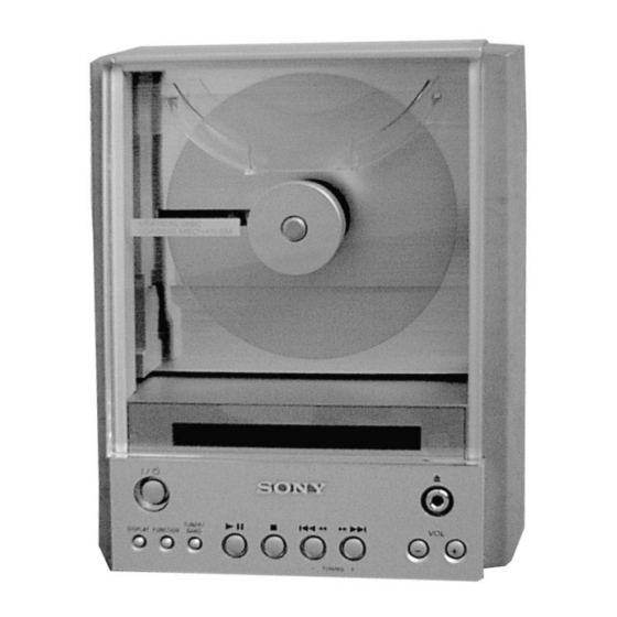
HCD-EX1 is the amplifier, CD and
tuner section in CMT-EX1.
MICROFILM
HCD-EX1
Model Name Using Similar Mechanism NEW
Mechanism Type
Base Unit Type
Optical Pick-up Type
SPECIFICATIONS
COMPACT COMPONENT SYSTEM
US Model
Canadian Model
AEP Model
UK Model
E Model
Australian Model
Tourist Model
CDM-60
KSM-770ACA/S-NP
KSS-770A/S-N1
1
Advertisement
Table of Contents

Related Manuals for Sony HCD-EX1


Summary of Contents for Sony HCD-EX1
- Page 1 US Model Canadian Model AEP Model UK Model E Model Australian Model Tourist Model HCD-EX1 is the amplifier, CD and tuner section in CMT-EX1. Model Name Using Similar Mechanism NEW Mechanism Type CDM-60 Base Unit Type KSM-770ACA/S-NP Optical Pick-up Type...
-
Page 2: Leakage Test
REPLACE THESE COMPONENTS WITH SONY PARTS FONCTIONNEMENT. NE REMPLACER CES COMPOSANTS WHOSE PART NUMBERS APPEAR AS SHOWN IN THIS QUE PAR DES PIÈCES SONY DONT LES NUMÉROS MANUAL OR IN SUPPLEMENTS PUBLISHED BY SONY. SONT DONNÉS DANS CE MANUEL OU DANS LES... -
Page 3: Table Of Contents
TABLE OF CONTENTS NOTES ON HANDLING THE OPTICAL PICK-UP BLOCK OR BASE UNIT 1. SERVICING NOTE ............4 The laser diode in the optical pick-up block may suffer electrostatic 2. GENERAL ................7 break-down because of the potential difference generated by the charged electrostatic load, etc. -
Page 4: Servicing Note
SECTION 1 SERVICING NOTE ADJUSTMENT OF CAM PHASE Absorber Absorber Boss SW lever Boss SW lever Rotate the cam in the arrow direction, and adjust the Insert the cam so that the boss touches the SW lever phase until the boss touches the SW lever shown in at the left shown in the figure. - Page 5 Shipment Mode • Mode for setting the state of the unit to the state at shipment. When returning the unit to the customer after completing servicing, set to the shipment mode. Procedure : Connect the power plug to the outlet while pressing the 1/u button. Change-over of AM tuner Step between 9kHz and 10kHz.
- Page 6 Displaying the CD Text • This unit is equipped with a simple CD text display function. The text is displayed only for the first 20 songs. As it will not be displayed from the 21st song, do not suspect a fault. In some cases, special characters may not be displayed or may be substituted by other characters.
-
Page 7: General
SECTION 2 GENERAL Front Panel LOCATION OF PARTS AND CONTROLS 1 1/u (power) button 2 DISC tray 3 Display window 4 6 button 5 VOLUME + button 6 VOLUME – button 7 )+/TUNING + button 8 =0/TUNING – button 9 p (stop) button 10 ^ button 11 TUNER/BAND button 12 FUNCTION button... - Page 8 This section is extracted from instruction manual.
-
Page 9: Disassembly
SECTION 3 DISASSEMBLY Note: Follow the disassembly procedure in the numerical order given. 3-1. BACK COVER AND CASE Case Two screws (KTP3x8) Two screws (BVTT3x5) Two screws (KTP3x8) Top panel Rear cover Side ornamental Two claws Screw (KTP3x8) !¡ Side ornamental 3-2. -
Page 10: Amp Block
3-3. AMP BLOCK Screw (BVTT3x5) Connector AMP board: CN801 AMP block Connector AMP board: CN810 Connector AMP board: CN802 Screw (BVTT3x5) Screw (BVTT3x5) 3-4. CD BLOCK CD block Connector MAIN board: CN351 Flat type wire (16 core) Screw (BVTT3x5) Connector MAIN board: CN301 Screw (BVTT3x5) Two screws (BVTT3x5) -
Page 11: Motor Assy And Cam
3-5. MOTOR ASSY AND CAM Note: Adjustment of the phase is required in assembly.Refer to "Section 1. Servicing Note" for details. Two screws (2.4x6) Slider (2) Two screws (BVTP2.6x8) Two screws (2.4x6) Screws (PTPWH2.6x?) Diskholder Lever (1) !¡ Two screws (BVTP2.6x8) !™... -
Page 12: Main Board And Power Board
3-7. MAIN BOARD AND POWER BOARD Main board Flat type wire (7 core) Spacer !¶ Back panel Flat type wire (13 core) Screw (BVTT3x5) !¢ Two screws (BVTP3x8) Screw (PTPWH2.6) Two screws Two screws Two screws (BVTT3x5) (BVTP3x8) (BVTT3x5) !¡ Screw (BVTT3x5) !§... -
Page 13: Electrical Adjustment
SECTION 4 ELECTRICAL ADJUSTMENT Note: Clear RF signal waveform means that the shape “◊” can be Note: clearly distinguished at the center of the waveform. 1. CD Block is basically constructed to operate without adjustment. Therefore, check each item in order given. RF signal waveform 2. -
Page 14: Diagrams
SECTION 5 DIAGRAMS 5-1. CIRCUIT BOARDS LOCATION MAIN BOARD LED BOARD AMP BOARD PANEL BOARD REG BOARD SW BOARD POWER BOARD LOADING BOARD... - Page 15 HCD-EX1 WAVEFORMS THIS NOTE IS COMMON FOR PRINTED WIRING – MAIN (1/3) SECTION – BOARDS AND SCHEMATIC DIAGRAMS. (In addition to this, the necessary note is printed in each block.) 3.1Vp-p For schematic diagrams. Note: • All capacitors are in µF unless otherwise noted. pF: µµF 16.9MHz...
-
Page 16: Printed Wiring Board - Main Section
HCD-EX1 5-2. PRINTED WIRING BOARD – MAIN SECTION – • See page 14 for Circuit Boards Location. • Semiconductor Location Ref. No. Location D139 D701 D751 D752 D753 D754 IC111 IC301 IC302 IC303 IC304 IC391 IC451 IC501 IC701 IC751 Q113... - Page 17 HCD-EX1...
-
Page 18: Schematic Diagram - Main (1/3) Section
HCD-EX1 5-3. SCHEMATIC DIAGRAM – MAIN (1/3) SECTION – • See page 15 for Waveforms. • See page 16 for Printed Wiring Board. • See page 30 for IC Block Diagrams. • See page 32 for IC Pin Functions. (Page 21) -
Page 19: Schematic Diagram - Main (2/3) Section
HCD-EX1 5-4. SCHEMATIC DIAGRAM – MAIN (2/3) SECTION – • See page 16 for Printed Wiring Board. (Page 18) (Page 20) MICON INTERFACE (Page 20) (Page 20) (Page 20) (Page 20) (Page 25) -
Page 20: Schematic Diagram - Main (3/3) Section
HCD-EX1 5-5. SCHEMATIC DIAGRAM – MAIN (3/3) SECTION – • See page 15 for Waveforms. • See page 16 for Printed Wiring Board. • See page 34 for IC Pin Functions. (Page 19) (Page 19) (Page 19) (Page 19) (Page 19) -
Page 21: Printed Wiring Board - Led/Loading/Sw Section
HCD-EX1 5-7. PRINTED WIRING BOARD – LED/LOADING/SW SECTION – 5-6. SCHEMATIC DIAGRAM – LED/LOADING/SW SECTION – • See page 14 for Circuit Boards Location. • See page 31 for IC Block Diagrams. (Page 18) (Page 28) -
Page 22: Printed Wiring Board - Amp Section
HCD-EX1 5-8. PRINTED WIRING BOARD – AMP SECTION – • See page 14 for Circuit Boards Location. (Page 28) (Page 16) (Page 28) -
Page 23: Schematic Diagram - Amp Section
HCD-EX1 5-9. SCHEMATIC DIAGRAM – AMP SECTION – (Page 20) (Page 29) (Page 29) -
Page 24: Printed Wiring Board - Panel Section
HCD-EX1 5-10. PRINTED WIRING BOARD – PANEL SECTION – • See page 14 for Circuit Boards Location. (Page 16) -
Page 25: Schematic Diagram - Panel Section
HCD-EX1 5-11. SCHEMATIC DIAGRAM – PANEL SECTION – (Page 19) -
Page 26: Printed Wiring Board - Power Section
HCD-EX1 5-12. PRINTED WIRING BOARD – POWER SECTION – • See page 14 for Circuit Boards Location. • Semiconductor Location Ref. No. Location D901 D911 D931 D941 IC933 IC951 (Page 28) Q951... -
Page 27: Printed Wiring Board - Power Section
HCD-EX1 5-13. SCHEMATIC DIAGRAM – POWER SECTION – (Page 29) -
Page 28: Printed Wiring Board - Reg Section
HCD-EX1 5-14. PRINTED WIRING BOARD – REG SECTION – • See page 14 for Circuit Boards Location. (Page 22) (Page 22) (Page 26) (Page 16) -
Page 29: Schematic Diagram - Reg Section
HCD-EX1 5-15. SCHEMATIC DIAGRAM – REG SECTION – (Page 23) (Page 27) (Page 20) -
Page 30: Ic Block Diagrams
HCD-EX1 5-16. IC BLOCK DIAGRAMS IC303 CXD2585Q • MAIN Board (1/3) 71 70 67 66 65 64 63 62 61 IC301 CXA2568M-T6 Digital APC PD AMP LC/PD VPCO LD_ON DVDD0 Clock V16M Generator XRST HOLD VCTL AGCVTH VREF APC LD AMP... -
Page 31: Loading Board
• LOADING Board IC351 LB1641 T.S.D O.C.P MOTOR MOTOR DRIVE DRIVE FWD/REV/STOP CONTROL LOGIC... -
Page 32: Ic Pin Functions
5-17. IC PIN FUNCTIONS • IC303 DIGITAL SERVO & DIGITAL SIGNAL PROCESSOR (CXA2585Q) (MAIN Board (1/3)) Pin Name Function Pin No. DVDD – Digital power supply XRST System reset “L” : reset MUTE Muting input “H” : mute DATA Serial data input, supplied from CPU XLAT Latch input, supplied from CPU CLOK... - Page 33 Pin No. Pin Name Function Tracking error signal input Center servo analog input RFDC RF signal input Test pin (Not used) ADIO – Analog ground AVSS0 Stabilized current input for operational amplifiers IGEN – Analog power supply AVDD0 EFM full swing output ASYO Asymmetry comparate voltage input ASYI...
- Page 34 • IC701 uCOM (UPD780306GF-024-3BA) (MAIN Board (3/3)) Pin No. Pin Name Function TUNED ST tuning PLL_CE ST PLL CE PLL_DATAI ST PLL IN data PLL_DATAO ST PLL OUT data PLL_CLK ST PLL CLK – Ground (Programing) XOUT – 5MHz (Main clock) –...
- Page 35 Pin No. Function Pin Name 51 to 54 COM0 to COM3 LCD COMMON BIAS LCD DRIVE POWER 56 to 58 VLC0 to VLC2 LCD DRIVER POWER VSS0 Ground 60 to 99 SEG0 to SEG39 FL segment signal output STEREO STEREO...
-
Page 36: Exploded Views
Ref. No. Part No. Description Remark Ref. No. Part No. Description Remark 4-969-961-11 EMBLEM(NO.4), SONY 4-222-709-01 YOKE(ST) 4-222-620-01 RING (EJECT) 4-222-704-01 STABILIZER 4-222-713-01 PANEL(BASE), FRONT 4-222-720-01 BUTTON(PLAY) 4-222-711-01 PLATE(L), SIDE 4-222-719-01 BUTTON(POWER) 4-222-710-01 PLATE(R), SIDE 4-985-672-01 SCREW(+PTPWHM2.6), FLOATING... -
Page 37: Chassis Section
6-2. CHASSIS SECTION not supplied not supplied not supplied 66 59 not supplied not supplied not supplied (US/CND) not supplied not supplied not supplied (UK) (AEP/UK) not supplied (HK) (AUS) Les composants identifiés par une The components identified by marque ! sont critiques pour la mark ! or dotted line with mark ! are critical for safety. -
Page 38: Mechanism Section
6-3. MECHANISM SECTION 104 124 not supplied Ref. No. Part No. Description Remark Ref. No. Part No. Description Remark 4-222-746-01 PLATE (CD) (LOWER), ORNAMENTAL 4-222-688-01 HOLDER, DISC 4-222-745-01 PLATE (CD) (UPPER), ORNAMENTAL 4-222-813-01 SLIDER (2) 4-222-701-01 PANEL, MECHANICAL 4-225-227-01 SPRING (ABSORBER),TENSION COIL 4-985-672-31 SCREW (+PTPWHM2.6), FLOATING 4-225-228-01 CAM(A) 4-222-697-01 RUBBER, FLOATING... -
Page 39: Base Unit Section
6-4. BASE UNIT SECTION not supplied not supplied Les composants identifiés par une The components identified by marque ! sont critiques pour la mark ! or dotted line with mark ! are critical for safety. sécurité. Replace only with part number Ne les remplacer que par une specified. -
Page 40: Electrical Parts List
SECTION 7 ELECTRICAL PARTS LIST Note: • Due to standardization, replacements in the parts list • SEMICONDUCTORS The components identified by In each case, u: µ , for example: may be different from the parts specified in the mark ! or dotted line with mark uA...: µ... - Page 41 LOADING MAIN Ref. No. Part No. Description Remark Ref. No. Part No. Description Remark 1-674-908-11 LOADING BOARD C167 1-126-964-11 ELECT 10uF C168 1-126-964-11 ELECT 10uF ************** C169 1-163-006-11 CERAMIC CHIP 560PF < CAPACITOR > C170 1-136-165-00 MYLAR 0.1uF C171 1-136-165-00 MYLAR 0.1uF C351 1-104-665-11 ELECT...
- Page 42 MAIN Ref. No. Part No. Description Remark Ref. No. Part No. Description Remark C384 1-163-011-11 CERAMIC CHIP 0.0015uF 10% < CONNECTOR > C391 1-104-665-11 ELECT 100uF C392 1-163-038-91 CERAMIC CHIP 0.1uF CN301 1-770-168-11 CONNECTOR,FFC(LIF(NON-ZIF))16P CN302 1-779-977-11 PIN, CONNECTOR 6P C401 1-163-009-11 CERAMIC CHIP 0.001uF CN303...
- Page 43 MAIN Ref. No. Part No. Description Remark Ref. No. Part No. Description Remark Q551 8-729-107-46 TRANSISTOR 2SC3624A-T1L15L16 R334 1-216-077-91 RES,CHIP 1/10W Q751 8-729-120-28 TRANSISTOR 2SC3052EF-T1-LEF R335 1-216-085-00 METAL CHIP 1/10W Q771 8-729-900-53 TRANSISTOR DTC114EKA-T146 R336 1-216-073-00 METAL CHIP 1/10W Q772 8-729-600-22 TRANSISTOR 2SA1235TP-1EF R337...
- Page 44 MAIN PANEL Ref. No. Part No. Description Remark Ref. No. Part No. Description Remark R552 1-216-073-00 METAL CHIP 1/10W < DIODE > R553 1-216-089-91 RES,CHIP 1/10W R554 1-216-025-91 RES,CHIP 1/10W D604 8-719-069-45 DIODE SELU5E23C-TP15 R555 1-216-049-91 RES,CHIP 1/10W D605 8-719-069-45 DIODE SELU5E23C-TP15 D650 8-719-069-56 DIODE UDZS-TE17-6.2B R701...
- Page 45 POWER Ref. No. Part No. Description Remark Ref. No. Part No. Description Remark A-4426-744-A POWER BOARD, COMPLETE (US,CND) D901 8-719-043-52 DIODE F5KQ60 D911 8-719-043-52 DIODE F5KQ60 *********************** D931 8-719-210-21 DIODE 11EQS04-NTA2B A-4426-753-A POWER BOARD, COMPLETE (EXCEPT US,CND) D941 8-719-210-21 DIODE 11EQS04-NTA2B *********************** <...
- Page 46 HCD-EX1 POWER Ref. No. Part No. Description Remark Ref. No. Part No. Description Remark R953 1-249-420-11 CARBON 1.8K 1/4W F 1-674-909-11 SW BOARD R954 1-249-437-11 CARBON 1/4W ********** R955 1-249-425-11 CARBON 4.7K 1/4W F < SWITCH > R956 1-249-415-11 CARBON...