Table of Contents
Advertisement
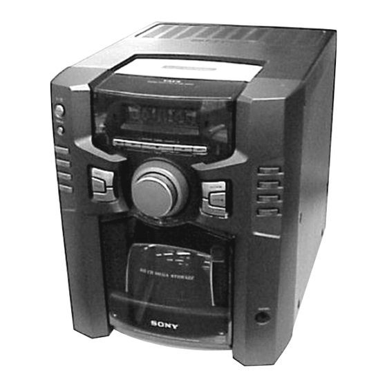
SERVICE MANUAL
Ver 1.2 2003. 10
HCD-GS100 is the Amplifier, CD player, Tape
Deck and Tuner section in MHC-GS100.
Amplifier section
U.S.A. model:
AUDIO POWER SPECIFICATIONS
POWER OUTPUT AND TOTAL
HARMONIC DISTORTION:
with 6 ohms loads both channels driven, from
120 – 10,000 Hz; rated 50 watts per channel
minimum RMS power, with no more than 10%
total harmonic distortion from 250 milliwatts to
rated output.
Continuous RMS power output
50 + 50 watts
(6 ohms at 1 kHz,
10% THD)
Total harmonic distortion less than 0.09%
(6 ohms at 1 kHz,
30 watts)
Inputs
VIDEO (MD) (phono jacks):
voltage 250 mV/450 mV,
impedance 47 kilohms
Outputs
PHONES (stereo phone jack):
accepts headphones of
8 ohms or more
SPEAKER:
accepts impedance of 6 to
16 ohms
Sony Corporation
9-873-554-03
2003J16-1
Home Audio Company
© 2003.10
Published by Sony Engineering Corporation
HCD-GS100
Model Name Using Similar Mechanism
CD Mechanism Type
CD
Section
Base Unit Name
Optical Pick-up Name
Model Name Using Similar Mechanism
TAPE
Section
Tape Transport Mechanism Type
SPECIFICATIONS
CD player section
System
Compact disc and digital
audio system
Laser
Semiconductor laser
(λ = 780 nm)
Emission duration:
continuous
Frequency response
2 Hz – 20 kHz (±0.5 dB)
Wavelength
780 – 790 nm
Signal-to-noise ratio
More than 90 dB
Dynamic range
More than 90 dB
Tape player section
Recording system
4-track 2-channel stereo
Frequency response
40 – 13,000 Hz (±3 dB),
using Sony TYPE I
cassette
Tuner section
FM stereo, FM/AM superheterodyne tuner
FM tuner section
Tuning range
87.5 – 108.0 MHz
Antenna
FM lead antenna
Antenna terminals
75 ohms unbalanced
Intermediate frequency
10.7 MHz
COMPACT DISC DECK RECEIVER
US Model
NEW
CDM64B-K1BD44B
BU-K1BD44B
KSM-213BFN
NEW
CMAL5Z2
AM tuner section
Tuning range
530 – 1,710 kHz
(with the interval set at
10 kHz)
531 – 1,710 kHz
(with the interval set at
9 kHz)
Antenna
AM loop antenna
Antenna terminals
External antenna terminal
Intermediate frequency
450 kHz
Speaker
Speaker system
3-way, bass-reflex type
Speaker units
Woofer:
13 cm, cone type
Tweeter:
5 cm, cone type
Super Tweeter:
2 cm, dome type
Nominal impedance
6 ohms
Approx. 210 × 325 ×
Dimensions (w/h/d)
241 mm
Mass
Approx. 2.8 kg net per
speaker
— Continued on next page —
Advertisement
Table of Contents

Related Manuals for Sony HCD-GS100


Summary of Contents for Sony HCD-GS100
- Page 1 HCD-GS100 SERVICE MANUAL US Model Ver 1.2 2003. 10 HCD-GS100 is the Amplifier, CD player, Tape Deck and Tuner section in MHC-GS100. Model Name Using Similar Mechanism CD Mechanism Type CDM64B-K1BD44B Section Base Unit Name BU-K1BD44B Optical Pick-up Name KSM-213BFN...
-
Page 2: Table Of Contents
HCD-GS100 General Power requirements: 120 V AC, 60 Hz Power consumption: 100 watts Dimensions (w/h/d) incl. projecting parts and controls: Approx. 280 × 325 × 465 mm Mass : Approx. 8.8 kg Supplied accessories: Remote commander (1) Batteries (2) AM loop antenna (1) -
Page 3: Leakage Test
COMPONENTS IDENTIFIED BY MARK 0 OR DOTTED LINE WITH MARK 0 ON THE SCHEMATIC DIAGRAMS AND IN THE PARTS LIST ARE CRITICAL TO SAFE OPERATION. REPLACE THESE COMPONENTS WITH SONY PARTS WHOSE PART NUMBERS APPEAR AS SHOWN IN THIS MANUAL OR IN SUPPLEMENTS PUBLISHED BY SONY. -
Page 4: Servicing Notes
HCD-GS100 SECTION 1 SERVICING NOTES CD-TEXT TEST DISC CLEANING OBJECTIVE LENS OF OPTICAL PICK-UP • In cleaning the objective lens of optical pick-up, be sure the following below. This unit is able to display the test data (character information) written in the CD on its fluorescent indicator tube. -
Page 5: General
HCD-GS100 SECTION 2 GENERAL This section is extracted from instruction manual. List of Button Locations and Reference Pages Main unit ALPHABETICAL ORDER BUTTON DESCRIPTIONS =/1 (power) 1 A – Q R – Z m (rewind) 4 REC z PAUSE/START qa... -
Page 6: Remote Control
HCD-GS100 Remote Control ALPHABETICAL ORDER BUTTON DESCRIPTIONS @/1 (power) 4 A – Q R – Z n N (play)** 0 REC wd ALBM +/ALBM –* qd w; X (pause) 0 CD wg REPEAT 3 x (stop) 0 CD SYNC wf SLEEP 1 . -
Page 7: Disassembly
HCD-GS100 SECTION 3 DISASSEMBLY • This set can be disassembled in the order shown below. 3-1. CABINET TOP (Page 8) 3-15 CASSETTE HOLDER, 3-2. FRONT CABI ASSY MECH DECK (CMAL5Z2) (Page 8) (Page 15) 3-16. BELT 3-3. BACK PANEL ASSY... -
Page 8: Cabinet Top
HCD-GS100 3-1. Cabinet Top qd cabinet top 9 three screws (BVTP3 × 8) 6 two screws (BVTP3 × 8) 8 panel side (L) 5 three screws (BVTP3 × 8) 0 wire (flat type) (7 core) (CN309 ) 4 panel side (R) 2 two screws (BVTP3 ×... -
Page 9: Back Panel Assy
HCD-GS100 3-3. Back Panel Assy 2 two screws (BVTP3 × 10) back panel assy 4 four screws (BVTP3 × 10) 5 screw (BVTP3 × 10) 3 dc fan (M391) 0 screw (BVTP3 × 10) 1 connector 2p (CN705) 6 screw (BVTP3 × 10) 7 two screws (BVTP3 ×... -
Page 10: Amp Board
HCD-GS100 3-5. AMP Board 3 two screws (BVTP3 × 8) 2 screw (BVTP3 × 8) 4 AMP board 1 connector 6p (CN502) 3-6. POWER Board 4 POWER board 3 power, cord 2 two screws (BVTP4 × 8) 1 two screws... -
Page 11: Holder (Led-S), Bracket (Middle-R)
HCD-GS100 3-7. Holder (LED-S), Bracket (Middle-R), Power Bracket 6 bracket (middle-R) 5 two screws (BVTP3 × 8) 4 three screws (BVTP3 × 8) 2 screw (BVTP3 × 8) 8 three screws (BVTP3 × 8) 9 two screws (BVTP3 × 8) -
Page 12: Base Unit (Bu-K1Bd44B), D.sensor (Out) Board, T.sensor Board
HCD-GS100 3-9. Base Unit (BU-K1BD44B), D.SENSOR (OUT) Board, T.SENSOR Board 4 screw (BVTP3 × 8) 5 D.SENSOR (OUT) board 3 base unit (BU-K1BD44B) 2 bracket (top 60) 1 three screws (BVTP3 × 8) 6 three screws (BVTP3 × 8) 7 T.SENSOR board 3-10. -
Page 13: Cd Led Board
HCD-GS100 3-11. CD LED Board Opens to right and left and CD LED BOARD 3 CD LED board is removed upwards from a slot. 3-12. BU Holder Assy 1 tension spring (F1) 2 tension spring (F-2) 3 two screws (PTP2.6 × 8) -
Page 14: Cd Board
HCD-GS100 3-13. CD Board 5 parallel (FFC) (16 core) wire (CN102) 6 CD board 1 Remove two solders. 3 screw (P2 × 5) 2 Remove two solders. 3-14. OP Base Assy (KSM-213BFN) 3 Remove the optical pick-up (KSM-213BFN) in the direction of arrow B . -
Page 15: Cassette Holder, Mech Deck (Cmal5Z2)
HCD-GS100 3-15. Cassette Holder, Mech Deck (CMAL5Z2) 4 cassette holder 5 spring cst cabinet top mech deck (CMAL5Z2) 1 four screws (BVTP3 × 8) 3-16. Belt 1 two screws fly wheel mech deck (CMAL5Z2) *Cautions of an assembly 5 belt... -
Page 16: Display Board
HCD-GS100 3-17. DISPLAY Board 7 connector 2p (CN708) 9 DISPLAY board 4 nat 2 konb jog 3 cover jog 1 konb volume front panel assembly 6 nine screws 8 connector 2p (S901) (BVTP2.6 × 8) 3-18. KEY Board 2 KEY board 1 two screws (BVTP2.6 ×... -
Page 17: Headphone Board
HCD-GS100 3-19. HEADPHONE Board 2 decoration panel 1 screw (BVTP2.6 × 8) 3 HEADPHONE board... -
Page 18: Test Mode
HCD-GS100 SECTION 4 TEST MODE [Panel Test Mode] [CD Service Mode] Procedure: • This mode can run the CD sled motor optionally. Use this mode, [MENU] [DISPLAY] 1. Press three buttons of , and simulta- for instance, when cleaning the optical pick-up. -
Page 19: Mechanical Adjustments
HCD-GS100 SECTION 5 SECTION 6 MECHANICAL ADJUSTMENTS ELECTRICAL ADJUSTMENTS • TAPE MECHANISM DECK SECTION DECK SECTION 0 dB = 0.775 V Precaution 1. Clean the following parts with a denatured alcohol-moistened Precaution swab: 1. Demagnetize the record/playback head with a head demagne-... - Page 20 HCD-GS100 Record/Playback Head Azimuth Adjustment Adjustment Location: Record/Playback/Erase Head Procedure: 1. Mode: Playback test tape AMP board Head azimuth P-4-A100 FRONT SPEAKER terminal (J501) adjustment screw (10 kHz, – 10 dB) L-CH, R-CH level meter – 2. Turn the adjustment screw and check output peaks. If the peaks do not match for L-CH and R-CH, turn the adjustment screw so that outputs match within 1dB of peak.
- Page 21 HCD-GS100 RFDC signal waveform CD SECTION VOLT/DIV: 200 mV TIME/DIV: 500 ns Note: 1. CD Block is basically designed to operate without adjustment. There- fore, check each item in order given. 2. Use YEDS-18 disc (3-702-101-01) unless otherwise indicated. level: 1.15 ± 0.35 Vp-p 3.
- Page 22 HCD-GS100 E-F Balance Check Checking Location: Connection: – CD BOARD (Conductor Side) – oscilloscope CD board TP (TE) TP (DVC) – Procedure: Connect an oscilloscpe to test point TP (TE) and TP (DVC) on TP (VC) the CD board. Turn the power on.
-
Page 23: Diagrams
HCD-GS100 SECTION 7 DIAGRAMS 7-1. Circuit Boards Location • Waveforms – CD Board – – MAIN Board – – DISPLAY Board – AMP board IC103 qg (RFAC) IC801 qa (SUBXOUT) IC701 id (X1) (CD Play Mode) D.SENSOR (OUT) board CD board 4Vp-p 1.05Vp-p... -
Page 24: Block Diagrams
HCD-GS100 7-2. Block Diagrams – CD Section – FILTER IC101 (1/2) DIGITAL SIGNAL PROCESSOR, DIGITAL FILTER, D/A CONVERTER IC103 56 53 RF AMP, FOCUS/TRACKING ERROR AMP DETECTOR CD +5V PCMD INTERFACE LRCK C2PO RFAC RFAC RFAC ASYMMETRY DIGITAL SUMMING CORRECTION... -
Page 25: Tuner/Tape Deck Section
HCD-GS100 – TUNER/TAPE DECK Section – AM ANT AM/FM IF, MPX TUNER AM RF-IN L-CH L-OUT AMP SECTION CFT1 AM DET OUT MPX IN AM OSC L-OUT L-IN AM MIX AM IF R-OUT R-CH MPX OUT R-OUT R-IN FM MIX FM DET 10.7MHz... -
Page 26: Amp Section
HCD-GS100 – AMP Section – J882 PHONES IC301 INPUT SELECTOR,VOLUME,DBFB J501 CD-L INB1 OUT1 SECTION IC501 – FRONT SPEAKER TUNER POWER AMP IMPEDANCE TUNER L-CH R-CH INC1 BB_A1 USE 6-16Ω SECTION Q101 – TAPE D301 DBFB SWITCH PB-L TAPE RY501... -
Page 27: Display/Power Supply Section
HCD-GS100 – DISPLAY/POWER Supply Section – IC701 DISPLAY CONTROLLER S751 – 754 FUNCTION KEY FL701 FLUORESCENT S770 – 776 INDICATOR TUBE FUNCTION KEY S760 – 762, 765, 768, 769, 780,781 FUNCTION KEY Q701 D742, 743 RV752 LED1/PIP1 68 PA4 LED DRIVE... -
Page 28: Printed Wiring Board - Cd Section
HCD-GS100 7-3. Printed Wiring Board – CD Section – • See page 23 for Circuit Boards Location. • Semiconductor Location Ref. No. Location D101 IC101 IC102 IC103 Q101 Q102 TP (VC) IC102 IC103 TP (RFAC) TP (DVC) IC101... -
Page 29: Schematic Diagram - Cd Section
HCD-GS100 7-4. Schematic Diagram – CD Section – • See page 42 for IC Block Diagrams. • See page 43 for IC Pin Function Description. • See page 23 for Wavefoms. KSM-213BFN... -
Page 30: Cd Motor/Sensor Section
HCD-GS100 7-5. Printed Wiring Board – CD MOTOR/SENSOR Section – • See page 23 for Circuit Boards Location. • Semiconductor Location Ref. No. Location D841 IC11 IC12 IC13 Q841 IC11 M441 M442 IC12 IC13... -
Page 31: Cd Motor/Sensor Section
HCD-GS100 7-6. Schematic Diagram – CD MOTOR/SENSOR Section – (Page 33) (Page 33) (Page 33) (Page 33) (Page 33) -
Page 32: Printed Wiring Board - Main Section
HCD-GS100 7-7. Printed Wiring Board – MAIN Section – • See page 23 for Circuit Boards Location. TUNER PACK (TCB-MG (U) ASSY) IC481 IC301 IC932 IC931 IC933 J301 IC801 IC802 IC803 IC401 • Semiconductor Location Ref. No. Location Ref. No. Location Ref. No. Location Ref. No. Location Ref. -
Page 33: Schematic Diagram - Main Section (1/3)
HCD-GS100 7-8. Schematic Diagram – MAIN Section (1/3) – • See page 42 for IC Block Diagrams. -
Page 34: Schematic Diagram - Main Section (2/3)
HCD-GS100 • See page 45 for IC Pin Function Description. • See page 23 for Wavefoms. 7-9. Schematic Diagram – MAIN Section (2/3) –... -
Page 35: Schematic Diagram - Main Section (3/3)
HCD-GS100 7-10. Schematic Diagram – MAIN Section (3/3) – H E A D ( R E C / P L AY / E R A S E ) -
Page 36: Printed Wiring Board - Amp Section
HCD-GS100 7-11. Printed Wiring Board – AMP Section – • See page 23 for Circuit Boards Location. J882 Q511 Q512 R522 R518 R515 R511 IC501 J501 • Semiconductor Location Ref. No. Location D502 D503 D508 D509 D510 D516 D518 D519... -
Page 37: Schematic Diagram - Amp Section
HCD-GS100 7-12. Schematic Diagram – AMP Section – Q512 2SC1623 -T1-L5L6 R550 R549 12.6 100k Q511 2SC1623-T1 -L5L6 R515 R511 100k Q511,512 THERMAL DETECT... -
Page 38: Printed Wiring Board - Display Section
HCD-GS100 7-13. Printed Wiring Board – DISPLAY Section – • See page 23 for Circuit Boards Location. • Semiconductor Location Ref. No. Location D701 D702 D704 D705 D706 D707 D742 J-12 IC702 D743 J-12 D752 D-10 D753 D758 A-12 IC701... -
Page 39: Schematic Diagram - Display Section
HCD-GS100 7-14. Schematic Diagram – DISPLAY Section – • See page 47 for IC Pin Function Description. • See page 23 for Wavefom. R E C PA U S E / S TA RT... -
Page 40: Printed Wiring Board - Power Section
HCD-GS100 7-15. Printed Wiring Board – POWER Section – • See page 23 for Circuit Boards Location. CNP902... -
Page 41: Schematic Diagram - Power Section
HCD-GS100 7-16. Schematic Diagram – POWER Section –... -
Page 42: Ic Block Diagrams
HCD-GS100 7-17. IC Block Diagrams – MAIN Board – – CD Board – IC101 CXD3017Q IC103 CXA2581N-T4 IC401 BA6780 RW/ROM DC OFST ERROR VIN1 VIN2 DIGITAL CORRECTOR RFDCI DIGITAL ASYMMETRY – CORRECTOR – RFDCO OPERATIONAL LRCK FIN1 AMPLIFIER FIN2 ANALOG SWITCH... -
Page 43: Ic Pin Function Description
HCD-GS100 7-18. IC Pin Function Description • CD Board IC101 CXD3017Q (Digital Signal Processor, Digital Servo Processor, Digital Filter, D/A Converter) Pin No. Pin Name Description SQSO Subcode Q data output to the system controller (IC801) SQCK Subcode Q data reading clock signal input from the system controller (IC801) XRST System reset signal input from the system controller (IC801) “L”: reset... - Page 44 HCD-GS100 Pin No. Pin Name Description RFDC RF signal input from the CXA2581N (IC103) ADIO Monitor output of the A/D converter input signal Not used (open) AVSS0 — Ground terminal (digital system) IGEN Stabilized current input for operational amplifiers AVDD0 —...
- Page 45 HCD-GS100 • MAIN Board IC801 M30622MGN-A02FP (System Controller) Pin No. Pin Name Description TABLE POS Table motor control signal output to the motor driver (IC401) LOAD POS Loading motor control signal output to the motor driver (IC401) LOAD NEG Loading motor control signal output to the motor driver (IC401)
- Page 46 HCD-GS100 Pin No. Pin Name Description PL-DATA Serial data output to the PROLOGIC IC Not used PL-CLK Serial clock ouput to the PROLOGIC IC Not used PL-RQ Request signal output to the PROLOGIC IC Not used VOL-CLK Clock output to the VOLUME IC (IC301)
- Page 47 HCD-GS100 • DISPLAY Board IC701 MB90M407APF-G-116-BND (Display Controller) Pin No. Pin Name Description LED16/PIP16 Grid drive signal output to the fluorescent indicator tube (FL701) FIP17 Not used 3 to 10 FIP18 to 25 Segment drive signal output to the fluorescent indicator tube (FL701) VSS-IO –...
-
Page 48: Exploded Views
HCD-GS100 Ver 1.1 2003.09 SECTION 8 EXPLODED VIEWS NOTE: • -XX, -X mean standardized parts, so they may • The mechanical parts with no reference number The components identified by mark 0 or have some differences from the original one. -
Page 49: Front Panel Section
HCD-GS100 8-2. Front Panel Section 71 77 including RV752 FL701 S791 Ref. No. Part No. Description Remark Ref. No. Part No. Description Remark 4-238-200-01 WINDOW, CD 4-224-104-41 DAMPER 4-238-198-01 HOLDER CD (A) 4-238-204-01 GEAR JOG 4-238-197-01 LID, CD 4-238-196-01 DECORATION PANEL... -
Page 50: Chassis Section
HCD-GS100 Ver 1.2 2003.10 8-3. Chassis Section F503 CDM64B-K1BD44B F504 F901 not supplied F902 supplied T901 not supplied not supplied Ref. No. Part No. Description Remark Ref. No. Part No. Description Remark 0 F504 1-684-156-11 CD LED BOARD 1-533-454-11 FUSE, GLASS TUBE (DIA. 5) (3.15A/125V) -
Page 51: Mechanism Deck Section (Cdm64B-K1Bd44B)
HCD-GS100 8-4. Mechanism Deck Section (CDM64B-K1BD44B) BU-K1BD44B not supplied M441 M442 Ref. No. Part No. Description Remark Ref. No. Part No. Description Remark 1-684-161-11 D.SENSOR(IN) BOARD 4-216-086-01 SPRING (F-2), TENSION 4-231-310-01 SLIDER (60) 4-957-577-21 SCREW PTP WH (2.6X8) (DIA. 10) -
Page 52: Base Unit Section (Bu-K1Bd44B)
HCD-GS100 8-5. Base Unit Section (BU-K1BD44B) Ref. No. Part No. Description Remark Ref. No. Part No. Description Remark A-4728-536-A CD BOARD, COMPLETE 1-823-005-11 CABLE, FLEXIBLE FLAT (21 CORE) 0 552 A-3328-818-A OPTICAL PICK-UP KSM-213BFN/C2NP 1-757-055-11 WIRE, PARALLEL (FFC) (16 CORE) -
Page 53: Electrical Parts List
HCD-GS100 SECTION 9 ELECTRICAL PARTS LIST NOTE: • Due to standardization, replacements in the • CAPACITORS: • SEMICONDUCTORS parts list may be different from the parts uF: µF In each case, u: µ, for example: specified in the diagrams or the components •... - Page 54 HCD-GS100 CD LED Ref. No. Part No. Description Remarks Ref. No. Part No. Description Remarks < RESISTOR > < THERMISTOR > R501 1-216-841-11 METAL CHIP 1/16W TH501 1-807-796-11 THERMISTOR R504 1-216-821-11 METAL CHIP 1/16W ************************************************************ R505 1-216-841-11 METAL CHIP 1/16W...
- Page 55 HCD-GS100 DISPLAY Ref. No. Part No. Description Remarks Ref. No. Part No. Description Remarks C171 1-115-412-11 CERAMIC CHIP 680PF 5.00% 25V R122 1-216-845-11 METAL CHIP 100K 1/16W C172 1-162-927-11 CERAMIC CHIP 100PF R123 1-216-833-11 METAL CHIP 1/16W C181 1-115-412-11 CERAMIC CHIP 680PF 5.00% 25V...
- Page 56 HCD-GS100 DISPLAY Ref. No. Part No. Description Remarks Ref. No. Part No. Description Remarks C722 1-126-960-11 ELECT 20.00% 50V R711 1-216-845-11 METAL CHIP 100K 1/16W C735 1-126-964-11 ELECT 10uF 20.00% 50V R712 1-216-845-11 METAL CHIP 100K 1/16W C737 1-126-964-11 ELECT 10uF 20.00% 50V...
- Page 57 HCD-GS100 D.SENSOR (IN) D.SENSOR (OUT) HEADPHONE L.T MOTOR LOAD SW MAIN Ref. No. Part No. Description Remarks Ref. No. Part No. Description Remarks 1-684-161-11 D.SENSOR(IN) BOARD A-4728-352-A MAIN BOARD, COMPLETE ****************** ********************* < TRANSISTOR > < CAPACITOR > Q841 8-729-921-53 PHOTO TRANSISTOR PT483F1...
- Page 58 HCD-GS100 MAIN Ref. No. Part No. Description Remarks Ref. No. Part No. Description Remarks C401 1-107-826-11 CERAMIC CHIP 0.1uF 10.00% 16V C953 1-126-964-11 ELECT 10uF 20.00% 50V C402 1-107-826-11 CERAMIC CHIP 0.1uF 10.00% 16V C954 1-126-967-11 ELECT 47uF 20.00% 50V...
- Page 59 HCD-GS100 MAIN Ref. No. Part No. Description Remarks Ref. No. Part No. Description Remarks < TRANSISTOR > R217 1-216-830-11 METAL CHIP 5.6K 1/16W R218 1-216-827-11 METAL CHIP 3.3K 1/16W Q101 8-729-120-28 TRANSISTOR 2SC1623-T1-L5L6 R219 1-216-833-11 METAL CHIP 1/16W Q102 8-729-036-89 TRANSISTOR...
- Page 60 HCD-GS100 MAIN POWER Ref. No. Part No. Description Remarks Ref. No. Part No. Description Remarks R447 1-216-833-11 METAL CHIP 1/16W R830 1-216-829-11 METAL CHIP 4.7K 1/16W R448 1-216-825-11 METAL CHIP 2.2K 1/16W R831 1-216-841-11 METAL CHIP 1/16W R451 1-216-833-11 METAL CHIP...
- Page 61 HCD-GS100 POWER T.SENSOR Ref. No. Part No. Description Remarks Ref. No. Part No. Description Remarks < TRANSFORMER > MISCELLANEOUS *************** 0 T902 1-437-726-11 TRANSFORMER, POWER 1-796-352-11 MECH DECK (W) < FUSE > A-2004-904-A TCB-MG (U) ASSY (TUNER PACK) 1-773-110-11 WIRE (FLAT TYPE) (19 CORE) 0 F901 1-533-450-11 FUSE, GLASS TUBE (DIA.
- Page 62 HCD-GS100 REVISION HISTORY Clicking the version allows you to jump to the revised page. Also, clicking the version at the upper right on the revised page allows you to jump to the next revised page. Ver. Date Description of Revision 2002.02...