Table of Contents
Advertisement
QQ
3 7 63 1515 0
SERVICE MANUAL
Ver 1.0 2004.03
• HCD-GX250 is the tuner, deck, CD and
amplifier section in MHC-GX250.
TE
L 13942296513
Amplifier section
AUDIO POWER SPECIFICATIONS
POWER OUTPUT AND TOTAL HARMONIC
DISTORTION:
With 6 ohm loads, both channels driven, from
120 – 10,000 Hz: rated 140 watts per channel
minimum RMS power, with no more than 10%
total harmonic distortion from 250 milliwatts to
rated output.
Continuous RMS power output (reference):
Total harmonic distortion less than 0.07% (6 ohms at
CD player section
System
Laser
Frequency response
Wavelength
Signal-to-noise ratio
Dynamic range
www
.
Sony Corporation
9-877-537-01
2004C1678-1
Home Audio Company
© 2004.03
Published by Sony Engineering Corporation
http://www.xiaoyu163.com
Tape deck section
Recording system
Frequency response
Tuner section
FM stereo, FM/AM superheterodyne tuner
FM tuner section
Tuning range
Antenna
140 + 140 watts (6 ohms at
Antenna terminals
1 kHz, 10% THD)
Intermediate frequency
1 kHz, 70 W)
AM tuner section
Tuning range
Compact disc and digital
audio system
Semiconductor laser
(λ=780 nm)
Emission duration:
Antenna
continuous
Antenna terminals
2 Hz – 20 kHz (±0.5 dB)
Intermediate frequency
780 – 790 nm
More than 90 dB
More than 90 dB
x
ao
u163
y
i
http://www.xiaoyu163.com
HCD-GX250
2 9
8
Model Name Using Similar Mechanism
CD
CD Mechanism Type
Section
Optical Pick-up Name
Tape deck
Model Name Using Similar Mechanism
Section
Tape Transport Mechanism Type
Q Q
3
6 7
1 3
1 5
SPECIFICATIONS
4-track 2-channel, stereo
50 – 13,000 Hz (±3 dB),
using Sony TYPE I
cassettes
87.5 – 108.0 MHz
(100-kHz step)
FM lead antenna
75 ohms unbalanced
10.7 MHz
530 – 1,710 kHz
(with the tuning interval
set at 10 kHz)
531 – 1,710 kHz
(with the tuning interval
set at 9 kHz)
AM loop antenna
External antenna terminal
450 kHz
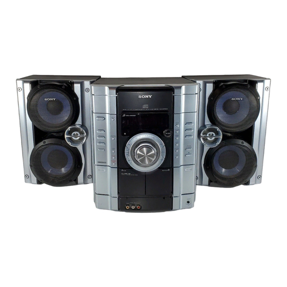
MINI HI-FI COMPONENT SYSTEM
co
.
9 4
2 8
US Model
Canadian Model
New
CDM74-K6BD80
KSM-213DCP/Z-NP
New
CWM43FF-05
0 5
8
2 9
9 4
2 8
General
Power requirements
120 V AC, 60 Hz
Power consumption
USA models:
205 watts
Canadian models:
260 VA
Dimensions (w/h/d) incl. projecting parts and
controls Amplifier/Tuner/Tape/CD section:
Approx. 280 × 327 ×
425 mm
Ma
ss
Approx. 10.0 kg
Design and specifications are subject to change
without notice.
m
9 9
9 9
Advertisement
Table of Contents

Related Manuals for Sony HCD-GX250


Summary of Contents for Sony HCD-GX250
- Page 1 HCD-GX250 3 7 63 1515 0 SERVICE MANUAL US Model Canadian Model Ver 1.0 2004.03 • HCD-GX250 is the tuner, deck, CD and amplifier section in MHC-GX250. Model Name Using Similar Mechanism CD Mechanism Type CDM74-K6BD80 Section Optical Pick-up Name...
-
Page 2: Leakage Test
LES COMPOSANTS IDENTIFÉS PAR UNE MARQUE 0 SUR LES DIAGRAMMES SCHÉMATIQUES ET LA LISTE DES PIÈCES SONT CRITIQUES POUR LA SÉCURITÉ DE FONCTIONNEMENT. NE REMPLACER CES COMPOSANTS QUE PAR DES PIÈSES SONY DONT LES NUMÉROS SONT DONNÉS DANS CE MANUEL OU DANS LES SUPPÉMENTS PUBLIÉS PAR SONY. -
Page 3: Table Of Contents
HCD-GX250 3 7 63 1515 0 TABLE OF CONTENTS NOTES ON HANDLING THE OPTICAL PICK-UP BLOCK OR BASE UNIT 1. SERVICING NOTE ·························································· 4 The laser diode in the optical pick-up block may suffer electrostatic 2. GENERAL ·········································································· 6 break-down because of the potential difference generated by the charged electrostatic load, etc. -
Page 4: Servicing Note
HCD-GX250 SECTION 1 SERVICING NOTE 3 7 63 1515 0 • SERVICE POSITION -1 (AMP BOARD) To inspect the AMP board, turn both of the front panel and the CD mechanism deck so that the left side of the product faces down. - Page 5 HCD-GX250 3 7 63 1515 0 • SERVICE POSITION -2 (BD80A BOARD) Remove the CD mechanism deck and place it on top of the pedestal as shown. Inspect the BD80A bard in this set up. BD80A board CD mechanism deck...
-
Page 6: General
HCD-GX250 SECTION 2 GENERAL 3 7 63 1515 0 List of button locations and reference pages How to use this page Illustration number Use this page to find the location of buttons and other TAPE A/B ed (18, 19, 20, 24) parts of the system that are mentioned in the text. -
Page 7: Setting The Clock
HCD-GX250 3 7 63 1515 0 Setting the clock Remote control ALPHABETICAL ORDER BUTTON DESCRIPTIONS Use buttons on the remote for the operation. ?/1 (power) 1 (8, 26) A – E Press ?/1 to turn on the system. m/M (rewind/fast forward) -
Page 8: Disassembly
HCD-GX250 SECTION 3 DISASSEMBLY 3 7 63 1515 0 Disassemble the unit in the order as shown below. Note: 3-1.COVER (TOP) (Page 9) 3-2.CD DOOR (Page 9) 3-3.FRONT PANEL SECTION (Page 10) 3-5.TAPE MECHANISM DECK, 3-6.PANEL BOARD 3-4.CD MECHANISM DECK... -
Page 9: Cover (Top)
HCD-GX250 3 7 63 1515 0 Note: Follow the disassembly procedure in the numerical order given. 3-1. COVER (TOP) qa two screws (+BVTP 3 × 10) qf cover (top) 6 two screws (Case 3 TP2) cover (Side-L) 8 screw (+BVTP 3 ×... -
Page 10: Front Panel Section
HCD-GX250 3 7 63 1515 0 3-3. FRONT PANEL SECTION 4 screw (+BVTP 3 × 8 ) 0 connector 3p (CN304C) 8 wire (flat type) 7 core (CN253) 6 connector 2p (CN805) 3 screw (+BVTP 3 × 10) 5 screw (+BVTP 3 × 8 ) qa connector 3p (CN102B) 2 screw (+BVTP 3 ×... -
Page 11: Tape Mechanism Deck, Game Jack Board
HCD-GX250 3 7 63 1515 0 3-5. TAPE MECHANISM DECK, GAME JACK BOARD 3 tape mechanism deck 2 six screws (+BVTP 2.6 × 8) 1 wire (flat type) 13 core (CN602) 5 GAME JACK board 4 two screws (+BVTP 2.6 × 8) L 13942296513 3-6. -
Page 12: Back Panel Section, Sub-Trans Board
HCD-GX250 3 7 63 1515 0 3-7. BACK PANEL SECTION, SUB-TRANS BOARD 9 back panel section 8 SUB-TRANS board 7 connector 2p (CN901) 6 two screws 5 three screws (+BVTT 3 × 10 ) (+BVTT 3 × 10) 1 connector... -
Page 13: Main Board
HCD-GX250 3 7 63 1515 0 3-9. MAIN BOARD 4 MAIN board 1 connector 10p (CN907) MAIN board 3 connector 13p (CN441) 2 two screws (+BVTP 3 × 8 ) L 13942296513 3-10. AMP BOARD 1 two screws (+BVTT 3 × 8 ) -
Page 14: Bd80A Board
HCD-GX250 3 7 63 1515 0 3-11. BD80A BOARD 3 screw (+BVTP 2.6 × 8 ) 1 wire (flat type) 17 core (CN201) 5 BD80A board 2 wire (flat type) 16 core (CN101) Remove soldering from the four points. -
Page 15: Driver Board, Sw Board
HCD-GX250 3 7 63 1515 0 3-13. DRIVER BOARD, SW BOARD 1 two screws (+BTTP (M2.6)) 3 connector 4p (CN703) 4 DRIVER board 5 screw (+BTTP (M2.6)) 6 SW board 2 wire (flat type) 5p (CN702) L 13942296513 3-14. OPTICAL PICK-UP (KSM-213DCP/Z-NP) 1 floating screw (+PTPWH M2.6) -
Page 16: Sensor Board
HCD-GX250 3 7 63 1515 0 3-15. SENSOR BOARD 1 floating screw (+PTPWH M2.6) 2 t ray 8 s crew (+BTTP (M2.6)) 3 b elt (table) 0 SENSOR board 4 floating screw (+PTPWH M2.6) 5 p ulley (table) 6 floating screw 9 connector (+PTPWH M2.6) -
Page 17: Motor (Ld) Board
HCD-GX250 3 7 63 1515 0 3-17. MOTOR (LD) BOARD 2 two screws (+BTTP (M2.6)) 4 Remove the two solderings of motor. 3 MOTOR (LD) board 5 l oading motor assy (M751) 1 b elt (loading) L 13942296513 u163... -
Page 18: Test Mode
HCD-GX250 SECTION 4 TEST MODE 3 7 63 1515 0 [Change-over of AM Tuner Step between 9 kHz and 2) Error display 10 kHz] Disc error • A step of AM channels can be changed over between 9 kHz and... - Page 19 HCD-GX250 3 7 63 1515 0 [PANEL Test Mode] [MC Test Mode] • All fluorecent segments and LEDs are tested. • This mode is used to test the function of the equalizer. • Keyboard check. Procedure: Procedure: 1. Press ?/1 button to turn the set ON.
- Page 20 HCD-GX250 3 7 63 1515 0 [CD Repeat 5 Times Limit Release Mode] Procedure: Press ?/1 button to turn the set ON. Select the function “CD”. Press three buttons x , CD and ENTER simultaneously. The message “LIMIT OFF” is displayed.
-
Page 21: Diagrams
HCD-GX250 SECTION 5 DIAGRAMS 3 7 6 3 1 5 1 5 0 Circuit Boards Location THIS NOTE IS COMMON FOR PRINTED WIRING BOARDS AND SCHEMATIC DIAGRAMS. (In addition to this, the necessary note is printed in each block.) -
Page 22: Block Diagrams - Panel Section
HCD-GX250 5-1. BLOCK DIAGRAMS – PANEL SECTION – 3 7 6 3 1 5 1 5 0 IC601(1/2) SYSTEM CONTROLLER S641-S650 Q610 FUNCTION STREM-LED1 25 KEY3 DRIVER LED851 S601-S608,S610-S612 FUNCTION 27 KEY1 S621-S624,S627-S630 FUNCTION 26 KEY2 S851 9 VOLUME-IN1... -
Page 23: Main Section
HCD-GX250 – MAIN SECTION – 3 7 6 3 1 5 1 5 0 IC101 IC441 IC102 JK441 SOUND PROCESSOR POWER AMP BUFFER RY441 CD-L 1 CDL VOUT2 Q481,Q482 BD/DRIVER CD-R SPEAKER SECTION VOUT1 R-CH R-CH OVERLOAD R-CH SWITCH... -
Page 24: Bd/Driver Section
HCD-GX250 – BD/DRIVER SECTION – 3 7 6 3 1 5 1 5 0 OPTICAL PICK-UP BLOCK (KSM-213DCP/Z-NP) IC101 DETECTOR RF AMP • R-CH is omitted due to same as L-CH +1.7V • Signal Path IC701 : CD (LD)MOTOR DRIVER... -
Page 25: Printed Wiring Board - Bd80A Section
HCD-GX250 5-2. PRINTED WIRING BOARD – BD80A SECTION – • See page 21 for Circuit Boards Location. • : Uses unleaded solder. 3 7 6 3 1 5 1 5 0 SPINDLE MOTOR (LIMIT) IC251 SLED MOTOR 1 3 9 4 2 2 9 6 5 1 3... -
Page 26: Schematic Diagram - Bd80A Section
HCD-GX250 5-3. SCHEMATIC DIAGRAM – BD80A SECTION – • See page 41 for IC PIN FUNCTION DESCRIPTION. 3 7 6 3 1 5 1 5 0 TP46 TP45 CN101 IOP1 IOP2 TP27 2SB1690K TOP1 JR111 TP014 TP17 TP18 JR105 TP19 0.001... -
Page 27: Printed Wiring Board - Cd Mechanism Section
HCD-GX250 5-4. PRINTED WIRING BOARD – CD MECHANISM SECTION – • See page 21 for Circuit Boards Location. 3 7 6 3 1 5 1 5 0 1 3 9 4 2 2 9 6 5 1 3 MAIN... -
Page 28: Schematic Diagram - Cd Mechanism Section
HCD-GX250 5-5. SCHEMATIC DIAGRAM – CD MECHANISM SECTION – 3 7 6 3 1 5 1 5 0 1 3 9 4 2 2 9 6 5 1 3 no mark : FM w w w u 1 6 3... -
Page 29: Printed Wiring Board - Main Section
HCD-GX250 5-6. PRINTED WIRING BOARD – MAIN SECTION – • See page 21 for Circuit Boards Location. • : Uses unleaded solder. 3 7 6 3 1 5 1 5 0 GAMEJACK DRIVER BOARD BOARD CN801 CN701 (Page 32) -
Page 30: Schematic Diagram - Main Section (1/2)
HCD-GX250 5-7. SCHEMATIC DIAGRAM – MAIN SECTION (1/2) – 3 7 6 3 1 5 1 5 0 R389 R390 R387 4.7k 4.7k R391 R151 R388 R392 4.7k Q101 2SC3052 R394 R393 R219 R152 R216 R217 R154 R153 C235... -
Page 31: Schematic Diagram - Main Section (2/2)
HCD-GX250 5-8. SCHEMATIC DIAGRAM – MAIN SECTION (2/2) – 3 7 6 3 1 5 1 5 0 Q362 2SC3052 C270 10 50V R362 R361 2.2k R364 Q361 4.7k 2SA1235 R363 4.7k R275 D316 R274 1SS355 Q315 2SC3052 Q314... -
Page 32: Printed Wiring Board - Panel Comb Section
HCD-GX250 5-9. PRINTED WIRING BOARD – PANEL COMB SECTION – • See page 21 for Circuit Boards Location. • : Uses unleaded solder. 3 7 6 3 1 5 1 5 0 PANEL BOARD CN603 (Page 34) (AMS- (AMS+... -
Page 33: Schematic Diagram - Panel Comb Section
HCD-GX250 5-10. SCHEMATIC DIAGRAM – PANEL COMB SECTION – 3 7 6 3 1 5 1 5 0 C830 C831 1000p 1000p S851 J801 JW275 ENCORDER JW276 SW851 CN252 SW ESE24SV CN254 CN804 C832 R852 1/8W JW272 R853 JW273... -
Page 34: Printed Wiring Board - Panel Section
HCD-GX250 5-11. PRINTED WIRING BOARD – PANEL SECTION – • See page 21 for Circuit Boards Location. • : Uses unleaded solder. 3 7 6 3 1 5 1 5 0 CONNECT BOARD CN253 (CHASSIS) (Page 32) (FLUORESCENT INDICATOR TUBE) -
Page 35: Schematic Diagram - Panel Section (1/2)
HCD-GX250 5-12. SCHEMATIC DIAGRAM – PANEL SECTION (1/2) – 3 7 6 3 1 5 1 5 0 R698 Q610 DTC143EKA -T146 CN604 JW601 JW602 R629 R628 D605 1SS355TE-17 R627 R854 R690 R639 D604 4.7k 1SS355TE-17 R691 C605 R641... -
Page 36: Schematic Diagram - Panel Section (2/2)
HCD-GX250 5-13. SCHEMATIC DIAGRAM – PANEL SECTION (2/2) – • See page 44 for IC PIN FUNCTION DESCRIPTION. 3 7 6 3 1 5 1 5 0 FL601 C623 C622 CN603 R710 R712 R778 R719 C620 R718 C621 LED601 3.3k... -
Page 37: Printed Wiring Board - Trans Section
HCD-GX250 5-14. PRINTED WIRING BOARD – TRANS SECTION – • See page 21 for Circuit Boards Location. • : Uses unleaded solder. 3 7 6 3 1 5 1 5 0 POWER TRANSFORMER POWER TRANSFORMER (MAIN) (SUB) BOARD CN442... -
Page 38: Printed Wiring Board - Amp Section
HCD-GX250 5-15. PRINTED WIRING BOARD – AMP SECTION – • See page 21 for Circuit Boards Location. • : Uses unleaded solder. 3 7 6 3 1 5 1 5 0 • Semiconductor Location SPEAKER Ref. No. Location (IMPEDANCE USE 6–16 ) -
Page 39: Schematic Diagram - Amp Power Section
HCD-GX250 5-16. SCHEMATIC DIAGRAM – AMP POWER SECTION – 3 7 6 3 1 5 1 5 0 PT901 F904 T8.0AL/125V CN905 FH908 FH907 FH910 FH909 F905 CN904 CN903 JW910 T8.0AL/125V FH912 F906 FH911 T3.15AL/125V JW909 JW902 FH914 F907... - Page 40 HCD-GX250 • IC BLOCK DIAGRAMS 3 7 6 3 1 5 1 5 0 IC101 BD3401KS2 (MAIN BOARD) IC251 BA5947FM (BD80A BOARD) CH4OUTR CH1PUTF TNF2 VOLOUT2 CH1OUTR BASS MIDDLE TREBLE CH4OUTF CH3OUTF CH2OUTF TNF1 BBNF2 PIN26 6.5k CH2OUTR CH3OUTR...
-
Page 41: Ic Pin Function Description
HCD-GX250 3 7 63 1515 0 5-17. IC PIN FUNCTION DESCRIPTION • IC101 CXD3058AR (RF AMP) (BD80A BOARD) Pin No Pin Name Description MIRR Mirror signal input/output (Not used) DFCT Defect signal input/output (Not used) Focus OK signal input/output (Not used) —... - Page 42 HCD-GX250 3 7 63 1515 0 Pin No. Pin Name Description Master PLL charge pump output AVDD5 — Analog power supply DDVROUT DC/DC converter output DDVRSEN DC/DC converter output voltage monitor pin AVSS5 — Analog ground DDCR DC/DC converter reset pin...
- Page 43 HCD-GX250 3 7 63 1515 0 Pin No. Pin Name Description CLOCK Serial data transfer clock input from CPU — Internal digital power supply SENS SENS output to CPU SCLK SENS serial data readout clock input ATSK Anti-shock input/output...
- Page 44 HCD-GX250 3 7 63 1515 0 • IC601 LC876972B-52S2-E (SYSTEM CONTROLLER) (PANEL BOARD) Pin No Pin Name Description O-MP3 CS CS output to CD Digital Processor(Not used) O-MP3 LP MOTER Motor signal output I-MP3 ACK SOL-B Motor signal input...
- Page 45 HCD-GX250 3 7 63 1515 0 Pin No Pin Name Description -VPP — Power supply (-) S8/METER-SW2 FL tube segment signal output S9/METER-SW3 FL tube segment signal output S10/SW1 FL tube segment signal output S11/SW2 FL tube segment signal output...
-
Page 46: Exploded Views
4-245-183-61 COVER (SIDE-L) (US) 1-693-631-12 TUNER (FM/AM) 4-245-183-71 COVER (SIDE-L) (CND) 1-400-285-11 F-BEAD, E2515 MRT 4-252-196-01 DOOR, CD 4-245-184-61 COVER (SIDE-R) (US) 3-038-018-01 EMBLEM, SONY 4-245-184-71 COVER (SIDE-R) (CND) 0 PT902 4-244-849-61 COVER (TOP) (US) X-4956-292-1 TRANS ASSY, SUB 4-244-849-71 COVER (TOP) (CND) -
Page 47: Front Panel Section
HCD-GX250 3 7 63 1515 0 6-2. FRONT PANEL SECTION not supplied not supplied not supplied supplied not supplied not supplied not supplied not supplied not supplied L 13942296513 not supplied not supplied not supplied not supplied not supplied not supplied Ref. -
Page 48: Main Board Section
HCD-GX250 3 7 63 1515 0 6-3. MAIN BOARD SECTION not supplied PT901 not supplied F904 F906 L 13942296513 F905 F907 not supplied Ref. No. Part No. Description Remarks Ref. No. Part No. Description Remarks 0 F904 4-242-527-01 S-SCREW, ITC+4-8 R 1-576-537-11 FUSE, GLASS TUBE (DIA.5) (T8.0AL/125V) -
Page 49: Cd Mechanism Deck Section -1 (Cdm74-K6Bd80)
HCD-GX250 3 7 63 1515 0 6-4. CD MECHANISM DECK SECTION -1 (CDM74-K6BD80) L 13942296513 M741 CD mechanism deck section-2 Ref. No. Part No. Description Remarks Ref. No. Part No. Description Remarks 4-218-253-21 SCREW (M2.6), +BTTP 4-243-820-01 GEAR (TABLE) -
Page 50: Cd Mechanism Deck Section -2 (Cdm74-K6Bd80)
HCD-GX250 3 7 63 1515 0 6-5. CD MECHANISM DECK SECTION -2 (CDM74-K6BD80) RE701 M751 L 13942296513 not supplied not supplied Ref. No. Part No. Description Remarks Ref. No. Part No. Description Remarks 1-687-135-12 DRIVER BOARD 4-231-189-01 PULLEY (B), CHUCKING 4-218-253-31 SCREW (M2.6), +BTTP... -
Page 51: Electrical Parts List
HCD-GX250 SECTION 7 1 STREAM LED ELECTRICAL PARTS LIST 3 7 63 1515 0 NOTE: • Due to standardization, replacements in the • COILS When indicating parts by reference number, parts list may be different from the parts uH: µH please include the board name. - Page 52 HCD-GX250 BD80A 3 7 63 1515 0 Ref. No. Part No. Description Remarks Ref. No. Part No. Description Remarks < RESISTOR > A-4750-181-A BD80A BOARD, COMPLETE ********************** R401 1-249-441-11 CARBON 100K 1/4W R402 1-249-441-11 CARBON 100K 1/4W < CAPACITOR >...
- Page 53 HCD-GX250 BD80A CONNECT DRIVER 3 7 63 1515 0 Ref. No. Part No. Description Remarks Ref. No. Part No. Description Remarks C251 1-162-969-11 CERAMIC CHIP 0.0068uF 10% R251 1-216-833-11 METAL CHIP 1/10W C252 1-164-360-11 CERAMIC CHIP 0.1uF R252 1-216-837-11 METAL CHIP...
- Page 54 HCD-GX250 DRIVER GAME JACK H/P JACK MAIN 3 7 63 1515 0 Ref. No. Part No. Description Remarks Ref. No. Part No. Description Remarks < IC > A-4750-771-A MAIN BOARD, COMPLETE ******************** IC701 8-759-598-69 IC BA6956AN IC712 8-759-598-69 IC BA6956AN 7-685-871-01 SCREW +BVTT 3X6 (S) <...
- Page 55 HCD-GX250 MAIN 3 7 63 1515 0 Ref. No. Part No. Description Remarks Ref. No. Part No. Description Remarks C152 1-130-475-00 MYLAR 0.0022uF 5% C274 1-162-949-11 CERAMIC CHIP 47uF 5.00% 50V C153 1-130-475-00 MYLAR 0.0022uF 5% C154 1-130-479-00 MYLAR 0.0047uF 5%...
- Page 56 HCD-GX250 MAIN 3 7 63 1515 0 Ref. No. Part No. Description Remarks Ref. No. Part No. Description Remarks D307 6-500-522-21 DIODE 10EDB40-TB3 Q315 8-729-120-28 TRANSISTOR 2SC3052F-T1-LF D308 6-500-522-21 DIODE 10EDB40-TB3 Q321 8-729-142-46 TRANSISTOR 2SC2001TP-LK D309 6-500-522-21 DIODE 10EDB40-TB3...
- Page 57 HCD-GX250 MAIN 3 7 63 1515 0 Ref. No. Part No. Description Remarks Ref. No. Part No. Description Remarks R158 1-216-825-11 METAL CHIP 2.2K 1/10W R247 1-216-833-11 METAL CHIP 1/10W R159 1-216-833-11 METAL CHIP 1/10W R248 1-216-833-11 METAL CHIP...
- Page 58 HCD-GX250 MAIN MOTOR (LD) MOTOR (TB) PANEL 3 7 63 1515 0 Ref. No. Part No. Description Remarks Ref. No. Part No. Description Remarks R377 1-216-833-11 METAL CHIP 1/10W C631 1-162-927-11 CERAMIC CHIP 100PF R378 1-216-833-11 METAL CHIP 1/10W...
- Page 59 HCD-GX250 PANEL 3 7 63 1515 0 Ref. No. Part No. Description Remarks Ref. No. Part No. Description Remarks < JUMPER RESISTOR > R629 1-216-150-91 RES-CHIP 1/8W R635 1-216-809-11 METAL CHIP 1/10W JR604 1-216-864-11 METAL CHIP 1/10W JR605 1-216-864-11 METAL CHIP...
- Page 60 HCD-GX250 PANEL 3 7 63 1515 0 Ref. No. Part No. Description Remarks Ref. No. Part No. Description Remarks R696 1-216-809-11 METAL CHIP 1/10W R769 1-216-845-11 METAL CHIP 100K 1/10W R697 1-216-809-11 METAL CHIP 1/10W R770 1-216-845-11 METAL CHIP...
- Page 61 HCD-GX250 PANEL SENSOR SUB-TRANS TRANS VIDEO OUT 3 7 63 1515 0 Ref. No. Part No. Description Remarks Ref. No. Part No. Description Remarks < VIBRATOR > C909 1-126-964-11 ELECT 10uF 20.00% 50V C910 1-126-968-11 ELECT 100uF 20.00% 50V X601 1-760-252-12 VIBRATOR, CRYSTAL (32.768kHz)
- Page 62 HCD-GX250 3 7 63 1515 0 Ref. No. Part No. Description Remarks 1-471-035-11 MAGNET ASSY 1-469-854-11 CORE, FERRITE 0 F904 1-576-537-11 FUSE, GLASS TUBE (DIA.5) (T8.0AL/125V) 0 F905 1-576-537-11 FUSE, GLASS TUBE (DIA.5) (T8.0AL/125V) 0 F906 1-533-451-11 FUSE, GLASS TUBE (DIA. 5) (T3.15AL/125V) 0 F907 1-533-451-11 FUSE, GLASS TUBE (DIA.
- Page 63 HCD-GX250 3 7 63 1515 0 MEMO L 13942296513 u163 http://www.xiaoyu163.com...
- Page 64 HCD-GX250 3 7 63 1515 0 REVISION HISTORY Clicking the version allows you to jump to the revised page. Also, clicking the version at the upper right on the revised page allows you to jump to the next revised page.