Table of Contents
Advertisement
HCD-GTX66/GTX77
QQ
3 7 63 1515 0
SERVICE MANUAL
Ver. 1.0 2007. 07
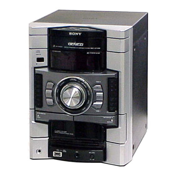
• HCD-GTX66/GTX77 are the tuner,
deck, CD and amplifier section in
MHC-GTX66/GTX77.
TE
L 13942296513
Amplifier section
Brazil model only
The following are measured at
AC 127 V or 220 V, 50/60 Hz
Front speaker
RMS output power:
HCD-GTX77: 300 W + 300 W
(at 4 Ω, 1 kHz, 10% THD)
HCD-GTX66: 280 W + 280 W
(at 4 Ω, 1 kHz, 10% THD)
Other models
The following are measured at
Mexican model:
HCD-GTX77: AC 127 V, 60 Hz
Other models:
AC 120, 220, 240 V, 50/60 Hz
Front speaker
Power Output (rated):
HCD-GTX77: 225 W + 225 W
(at 4 Ω, 1 kHz, 1% THD)
HCD-GTX66: 210 W + 210 W
(at 4 Ω, 1 kHz, 1% THD)
RMS output power (reference):
HCD-GTX77: 380 W + 380 W
(per channel at 4 Ω, 1 kHz,
10% THD)
HCD-GTX66: 340 W + 340 W
(per channel at 4 Ω, 1 kHz,
10% THD)
www
.
Sony Corporation
9-887-780-01
2007G04-1
Personal Audio Division
© 2007. 07
Published by Sony Techno Create Corporation
http://www.xiaoyu163.com
CD
Section
Tape Deck
Section
x
ao
u163
y
i
http://www.xiaoyu163.com
2 9
8
Model Name Using Similar Mechanism
CD Mechanism Type
Optical Pick-up Name
Model Name Using Similar Machanism
Q Q
3
6 7
1 3
1 5
SPECIFICATIONS
Inputs
VIDEO (AUDIO IN) L/R:
AUDIO (AUDIO IN) L/R:
MIC:
(USB) port:
Outputs
PHONES:
Disc player section
System
Laser
Laser Output
co
.
9 4
2 8
E Model
HCD-GTX88
CDM74KF-K6BD91UR-WOD//M
KSM-213DCP/C2NP
HCD-GTX88
0 5
8
2 9
9 4
2 8
Voltage 250 mV,
impedance 47 kilohms
Voltage 450 mV,
impedance 47 kilohms
Sensitivity 1 mV,
impedance 10 kilohms
Type A
accepts headphones of
8 ohms or more
Compact disc and digital
audio system
Semiconductor laser
(λ=770 – 810 nm)
Emission duration:
continuous
Max. 44.6 µW*
* This output is the value measured
at a distance of 200 mm from the
objective lens surface on the Optical
Pick-up Block with 7 mm aperture.
– Continued on next page –
m
CD DECK RECEIVER
9 9
9 9
1
Advertisement
Table of Contents

Related Manuals for Sony HCD-GTX66


Summary of Contents for Sony HCD-GTX66
- Page 1 RMS output power: HCD-GTX77: 300 W + 300 W MIC: Sensitivity 1 mV, (at 4 Ω, 1 kHz, 10% THD) impedance 10 kilohms HCD-GTX66: 280 W + 280 W (USB) port: Type A (at 4 Ω, 1 kHz, 10% THD) Outputs PHONES:...
- Page 2 COMPONENTS IDENTIFIED BY MARK 0 OR DOTTED LINE WITH MARK 0 ON THE SCHEMATIC DIAGRAMS AND IN THE PARTS LIST ARE CRITICAL TO SAFE OPERATION. REPLACE THESE COMPONENTS WITH SONY PARTS WHOSE PART NUMBERS APPEAR AS SHOWN IN THIS MANUAL OR IN SUPPLEMENTS PUBLISHED BY SONY.
- Page 3 HCD-GTX66/GTX77 3 7 63 1515 0 Notes on Chip Component Replacement NOTES ON LASER DIODE EMISSION CHECK • Never reuse a disconnected chip component. The laser beam on this model is concentrated so as to be focused on • Notice that the minus side of a tantalum capacitor may be the disc reflective surface by the objective lens in the optical pick- damaged by heat.
- Page 4 HCD-GTX66/GTX77 3 7 63 1515 0 MODEL IDENTIFICATION – MODEL NUMBER LABEL – PART No. MODEL PARTS No. GTX66 3-198-001-2s 3-113-126-2s L 13942296513 3-198-009-2s GTX77 3-198-001-1s 3-113-126-1s 3-198-009-1s • Abbreviation : Argentina model : 120V AC area in E model...
-
Page 5: Table Of Contents
HCD-GTX66/GTX77 3 7 63 1515 0 TABLE OF CONTENTS 1. GENERAL 6-7. Circuit Boards Location ............ 37 6-8. Printed Wiring Board — BD91 Section — ....... 40 Guide to parts and controls ............6 6-9. Schematic Diagram — BD91 Section — ......41 6-10. -
Page 6: General
HCD-GTX66/GTX77 SECTION 1 GENERAL 3 7 63 1515 0 This section is extracted from instruction manual. Guide to parts and controls This manual mainly explains operations using the buttons on the unit, but the same operations can also be performed using the buttons on the remote having the same or similar names. - Page 7 HCD-GTX66/GTX77 3 7 63 1515 0 1 FLANGER (pages 35, 43, 48) +/– (pages 17, 20, 23, 25, 27, DELAY (pages 35, 43, 48) Press to select a folder. CHORUS (pages 36, 43, 48) SOUND FLASH (page 35) m/M (rewind/fast forward) Press to create a party atmosphere.
- Page 8 HCD-GTX66/GTX77 3 7 63 1515 0 N REC/ERASE (indicator) X EQ BAND/MEMORY (page 33) (pages 23, 25) Press to select a frequency band when adjusting the graphic Lights up when recording from a disc equalizer. onto the connected optional USB...
- Page 9 HCD-GTX66/GTX77 3 7 63 1515 0 – Display AUTO PRESET MONO TUNED PLAY SLEEP FLANGER CHORUS DELAY SHUF TAPE USB SYNC MATRIX SUR 12 REP 1 LINK ALL 1 DISC S MP3 BOOSTER Z GROOVE USB MEMORY A Lights up when the USB function is K Indicators for the TAPE function selected (page 24).
- Page 10 HCD-GTX66/GTX77 3 7 63 1515 0 Subwoofer A (SS-WG88A) 1 "/1 (on/standby) (pages 13, 16, Press to turn the system on or off. B CLOCK/TIMER SELECT (page 38) CLOCK/TIMER SET (pages 16, Press to set the clock and the timers.
- Page 11 HCD-GTX66/GTX77 3 7 63 1515 0 E ./> (go forward/go J EQ (page 33) backward) (pages 17, 20, 23, 25, Press to select a preset sound effect. 27, 31, 37, 48) K CLEAR (pages 21, 27) Press to select a track.
-
Page 12: Disassembly
HCD-GTX66/GTX77 SECTION 2 DISASSEMBLY 3 7 63 1515 0 Note : Disassemble the unit in the order as shown below. 2-1. CASE (TOP) (Page 13) 2-2. LOADING PANEL (Page 13) 2-9. COVER (CDM) (Page 17) 2-3. TUNER PACK (Page 14) 2-16. -
Page 13: Case (Top)
HCD-GTX66/GTX77 3 7 63 1515 0 Note : Follow the disassembly procedure in the numerical order given. 2-1. CASE (TOP) 8 two screws (+BVTP 3 × 10) qa two screws (+BVTP 3 × 10) 0 panel (side-L) 7 two screws... -
Page 14: Tuner Pack
HCD-GTX66/GTX77 3 7 63 1515 0 2-3. TUNER PACK 2 wire (flat type) (9 core) (CN1) 3 tuner pack 1 two screws (+BVTP 3 × 8) L 13942296513 2-4. CD BLOCK SECTION qs CD block section 6 wire (flat type) (13 core) -
Page 15: Front Panel Section
HCD-GTX66/GTX77 3 7 63 1515 0 2-5. FRONT PANEL SECTION 5 wire (flat type) (11 core) 6 CN100 (4P) (CN509) 4 wire (flat type) (17 core) (CN508) 0 front panel section 9 CN903 (3P) 7 CN503 (3P) 8 CN507 (8P) -
Page 16: Panel Board, Function Board, Jog Board
HCD-GTX66/GTX77 3 7 63 1515 0 2-7. PANEL BOARD, FUNCTION BOARD, JOG BOARD 2 two screws (+BVTP 2.6 (3CR)) 8 five screws 4 PANEL board 3 two screws (+BVTP 2.6 (3CR)) (+BVTP 2.6 (3CR)) 1 CN956 (2P) 6 CN905 (2P) 9 four screws (+BVTP 2.6 (3CR)) -
Page 17: Cover (Cdm)
HCD-GTX66/GTX77 3 7 63 1515 0 2-9. COVER (CDM) CD mechanism deck 3 cover (CDM) 2 screw (+BVTP 3 × 10) 1 two screws (+BVTP 3 × 10) L 13942296513 2-10. BACK PANEL SECTION 3 CN1202 (2P) 4 wire (flat type) (17 core) -
Page 18: Power Board Section
HCD-GTX66/GTX77 3 7 63 1515 0 2-11. POWER BOARD SECTION 7 screw (+BV3 (3-CR)) 8 POWER board section 6 two screws (+BV3 (3-CR)) 5 screw (+BV3 (3-CR)) 3 two screws (+BVTP 3 × 10) 4 screw (+BVTP 3 × 10) -
Page 19: Subwoofer Board, Power Board
HCD-GTX66/GTX77 3 7 63 1515 0 2-13. SUBWOOFER BOARD, POWER BOARD 1 screw (+BV3 (3-CR)) 3 SUBWOOFER board 2 two screws (+BVTP 3 × 10) qs heat sink assy 8 two screws (+BVTP 3 × 8) qa bracket (PC) 0 screw (+BVTP 3 ×... -
Page 20: Bd91 Board
HCD-GTX66/GTX77 3 7 63 1515 0 2-15. BD91 BOARD 3 BD91 board 1 wire (flat type) (16 core) 2 Remove the four solders. (CN301) L 13942296513 2-16. DRIVER BOARD, SW BOARD, USB BOARD 1 two screws (+BVTT (M2.6)) 2 CN703 (4P) -
Page 21: Optical Pick-Up
HCD-GTX66/GTX77 3 7 63 1515 0 2-17. OPTICAL PICK-UP 7 optical pick-up (BU-K6BD91UR) 4 two insulators 6 two insulators 3 two coil springs (insulator) 5 two coil springs (insulator) 1 two floating screws (+PTPWH M2.6) 2 two floating screws (+PTPWH M2.6) -
Page 22: Motor (Tb) Board
HCD-GTX66/GTX77 3 7 63 1515 0 2-19. MOTOR (TB) BOARD 2 stopper table 1 stopper 7 t able motor assy (M741) 3 wire (flat type) (5 core) (CN742) 8 MOTOR (TB) board 6 Remove the two solderings of motor. -
Page 23: Test Mode
HCD-GTX66/GTX77 SECTION 3 TEST MODE 3 7 63 1515 0 4. When the [MASTER VOLUME] knob is turned clockwise even [GC TEST MODE] slightly, the sound volume increases to its maximum and a • This mode is used to check the fluorescent indicator tube, LEDs, message “VOLUME MAX”... - Page 24 HCD-GTX66/GTX77 3 7 63 1515 0 [CD SERVICE MODE] • Aging mode sequence: • This mode let you move the CD sled motor freely. Use this mode when you want to clean the optical pick-up. START Procedure: 1. Press ?/1 button to turn on the system.
- Page 25 HCD-GTX66/GTX77 3 7 63 1515 0 [CD ERROR CODE MODE] : The process when trouble occurs : Process ejecting DISC • Display the CD error code when an error occurred. : Process waiting for inserting DISC Procedure: : Process sending request to insert a disc to upper 1.
- Page 26 HCD-GTX66/GTX77 3 7 63 1515 0 [CD REPEAT 5 LIMIT OFF MODE] Procedure: 1. Press ?/1 button to turn on the system. • The number of repeat for CD playback is 5 times when the re- 2. Select CD section.
-
Page 27: Mechanical Adjustments
HCD-GTX66/GTX77 SECTION 4 MECHANICAL ADJUSTMENTS 3 7 63 1515 0 [ERROR MESSAGE] Precaution 1. Clean the following parts with a denatured alcohol-moistened swab: 1. GC error message record/playback heads pinch rollers erase head rubber belts • Display capstan idlers 2. -
Page 28: Electrical Adjustments
HCD-GTX66/GTX77 SECTION 5 ELECTRICAL ADJUSTMENTS 3 7 63 1515 0 0 dB = 1 µV 0 dB = 0.775 V TUNER SECTION DECK SECTION [FM Tune Level Check] 1. Demagnetize the record/playback head with a head demagnetizer. FM signal generator 2. - Page 29 HCD-GTX66/GTX77 3 7 63 1515 0 3. Mode: Playback CD SECTION test tape [TEST DISC LIST] P-4-A100 oscilloscope (10 kHz, –10 dB) Use the following test disc on test mode. pin 1 L-CH • CD: YEDS-18 (PART No. 3-702-101-01)
- Page 30 HCD-GTX66/GTX77 3 7 63 1515 0 [RF LEVEL CHECK] oscilloscope BD91 board TP123(RFO) TP124(VC) – Procedure : 1. Connect an oscilloscope to TP123 (RFO) and TP124 (VC). 2. Turn the power on. 3. Load a disc (YEDS-18) and playback.
-
Page 31: Diagrams
HCD-GTX66/GTX77 SECTION 6 DIAGRAMS 3 7 6 3 1 5 1 5 0 6-1. BLOCK DIAGRAM — RF/SERVO SECTION — CD+1.5V REG CD+1.5V DVDD+3.3V IC201 FNI1 CD LCH MAIN FPI1 SECTION CD RCH (Page 33) FNI2 DETECTOR FPI2 • Signal Path... -
Page 32: Block Diagram - Tape/Tuner Section
HCD-GTX66/GTX77 3 7 6 3 1 5 1 5 0 6-2. BLOCK DIAGRAM — TAPE/TUNER SECTION — DECK-A AIN1 L – CH EQ OUT1 PB OUT1 TAI1 MAIN TC-PB-L HEAD SECTION R – CH R-CH (Page 33) CN510 BIN1... -
Page 33: Block Diagram - Main Section
HCD-GTX66/GTX77 3 7 6 3 1 5 1 5 0 6-3. BLOCK DIAGRAM — MAIN SECTION — INPUT SELECT SWITCH, GRAPHIC EQUALIZER CONTROL, ELECTRICAL VOLUME IC101 RV1150 J103 SAOUT MIC AMP MIC AMP D-LIGHT IC1100 IC1100 D101,102 LEVEL J1100... -
Page 34: Block Diagram - Usb Section
HCD-GTX66/GTX77 3 7 6 3 1 5 1 5 0 6-4. BLOCK DIAGRAM — USB SECTION — USB CONTROL S-RAM IC901 IC921 VBUS POWER ON/OFF SWITCH VBUS+5V I/O0 IC915 I/O3 • I/O4 P00/D0 I/O7 P07/D7 P75/USBOC • • EN 1... -
Page 35: Block Diagram - Amp Section
HCD-GTX66/GTX77 3 7 6 3 1 5 1 5 0 6-5. BLOCK DIAGRAM — AMP SECTION — MAIN DBFB F/B SECTION J1101 (Page 33) PHONES POWER AMP IC601 D624 RY646 MAIN SECTION TM600 (Page 33) FRONT SPEAKER OVER LOAD... -
Page 36: Block Diagram - Display/Power Section
HCD-GTX66/GTX77 3 7 6 3 1 5 1 5 0 6-6. BLOCK DIAGRAM — DISPLAY/POWER SECTION — LED+9V 83 XI KEY2 X900 S901 – 915, 4MHz 917 –933 82 XO KEY0 Q903 Q902 P1 – 36 Q900 LED SELECTOR... -
Page 37: Circuit Boards Location
HCD-GTX66/GTX77 3 7 63 1515 0 6-7. CIRCUIT BOARDS LOCATION SENSOR board BD91 board SW board MOTOR (TB) board MOTOR (LD) board USB board DRIVER board PANEL board FUNCTION board JOG board USB CONNECTOR board L 13942296513 MAIN board... - Page 38 HCD-GTX66/GTX77 3 7 63 1515 0 • Note For Printed Wiring Boards And Schematic Diagrams Note on Printed Wiring Board: Note on Schematic Diagram: • X : parts extracted from the component side. • All capacitors are in µF unless otherwise noted. (p: pF) •...
- Page 39 HCD-GTX66/GTX77 3 7 6 3 1 5 1 5 0 • Waveforms — BD91 BOARD — (CD PLAY) — MAIN BOARD — IC101 5 (FEI) IC401 q; (XC-IN) Approx. 1 Vp-p 200 mVp-p 32.768 kHz 100 mV/DIV, 5 msec/DIV 0.5 V/DIV, 0.1 µ...
-
Page 40: Printed Wiring Board - Bd91 Section
HCD-GTX66/GTX77 3 7 6 3 1 5 1 5 0 6-8. PRINTED WIRING BOARD — BD91 SECTION — • Refer to page 37 for Circuit Boards Location. : Uses unleaded solder. M401 (SPINDLE) S201 (LIMIT) C404 C403 R402 M402... -
Page 41: Schematic Diagram - Bd91 Section
HCD-GTX66/GTX77 • Refer to page 39 for Waveforms. 3 7 6 3 1 5 1 5 0 • Refer to page 62 IC Block Diagrams. 6-9. SCHEMATIC DIAGRAM — BD91 SECTION — • Refer to page 67 for IC Pin Description of IC101. -
Page 42: Printed Wiring Boards - Driver Section
HCD-GTX66/GTX77 3 7 6 3 1 5 1 5 0 6-10. PRINTED WIRING BOARDS — DRIVER SECTION — • Refer to page 37 for Circuit Boards Location. : Uses unleaded solder. 1 3 9 4 2 2 9 6 5 1 3... -
Page 43: Schematic Diagram - Driver Section
HCD-GTX66/GTX77 3 7 6 3 1 5 1 5 0 6-11. SCHEMATIC DIAGRAM — DRIVER SECTION — • Refer to page 62 for IC Block Diagrams. IC B/D IC701 R702 R701 D701 C715 CN704 C751 CN721 M751 IC B/D... -
Page 44: Schematic Diagram - Main Section (1/4)
HCD-GTX66/GTX77 • Refer to page 39 for Waveforms. 3 7 6 3 1 5 1 5 0 • Refer to page 62 for IC Block Diagrams. 6-12. SCHEMATIC DIAGRAM — MAIN SECTION (1/4) — • Refer to page 69 for IC Pin Description of IC401. -
Page 45: Schematic Diagram - Main Section (2/4)
HCD-GTX66/GTX77 3 7 6 3 1 5 1 5 0 6-13. SCHEMATIC DIAGRAM — MAIN SECTION (2/4) — • Refer to page 62 for IC Block Diagrams. (Page 51) (Page 41) (Page 53) USB BOARD BD91 BOARD EFFECTOR BOARD... -
Page 46: Schematic Diagram - Main Section (3/4)
HCD-GTX66/GTX77 3 7 6 3 1 5 1 5 0 6-14. SCHEMATIC DIAGRAM — MAIN SECTION (3/4) — • Refer to page 64 for IC Block Diagrams. (Page 45) (Page 44) MAIN BOARD (1/4) MAIN BOARD (2/4) MAIN BOARD (3/4) -
Page 47: Schematic Diagram - Main Section (4/4)
HCD-GTX66/GTX77 3 7 6 3 1 5 1 5 0 6-15. SCHEMATIC DIAGRAM — MAIN SECTION (4/4) — • Refer to page 64 for IC Block Diagrams. (Page 44) (Page 45) MAIN BOARD (1/4) MAIN BOARD (2/4) MAIN BOARD (4/4) -
Page 48: Printed Wiring Board - Main Section
HCD-GTX66/GTX77 3 7 6 3 1 5 1 5 0 6-16. PRINTED WIRING BOARD — MAIN SECTION — • Refer to page 37 for Circuit Boards Location. : Uses unleaded solder. (Page 52) (Page 42) EFFECTOR (Page 50) (Page 56) -
Page 49: Printed Wiring Board - Usb Connector Section
HCD-GTX66/GTX77 3 7 6 3 1 5 1 5 0 6-17. PRINTED WIRING BOARD — USB CONNECTOR SECTION — 6-18. SCHEMATIC DIAGRAM — USB CONNECTOR SECTION — • Refer to page 37 for Circuit Boards Location. : Uses unleaded solder. -
Page 50: Printed Wiring Board - Usb Section
HCD-GTX66/GTX77 3 7 6 3 1 5 1 5 0 6-19. PRINTED WIRING BOARD — USB SECTION — • Refer to page 37 for Circuit Boards Location. : Uses unleaded solder. C902 C903 C904 CN904 R928 R921 IC915 C901... -
Page 51: Schematic Diagram - Usb Section
HCD-GTX66/GTX77 • Refer to page 39 for Waveforms. 3 7 6 3 1 5 1 5 0 • Refer to page 65 IC Block Diagrams. 6-20. SCHEMATIC DIAGRAM — USB SECTION — • Refer to page 72 for IC Pin Description of IC901. -
Page 52: Printed Wiring Board - Effector Section
HCD-GTX66/GTX77 3 7 6 3 1 5 1 5 0 6-21. PRINTED WIRING BOARD — EFFECTOR SECTION — • Refer to page 37 for Circuit Boards Location. : Uses unleaded solder. MAIN BOARD CN512 (Page 48) 1 3 9 4 2 2 9 6 5 1 3 •... -
Page 53: Schematic Diagram - Effector Section
HCD-GTX66/GTX77 3 7 6 3 1 5 1 5 0 6-22. SCHEMATIC DIAGRAM — EFFECTOR SECTION — • Refer to page 65 for IC Block Diagrams. 1 3 9 4 2 2 9 6 5 1 3 (Page 45) -
Page 54: Printed Wiring Board - Panel Section
HCD-GTX66/GTX77 3 7 6 3 1 5 1 5 0 6-23. PRINTED WIRING BOARD — PANEL SECTION — • Refer to page 37 for Circuit Boards Location. : Uses unleaded solder. PANEL BOARD JW966 JW965 JW967 Q920 JW939 JW968... -
Page 55: Schematic Diagram - Panel Section
HCD-GTX66/GTX77 • Refer to page 39 for Waveforms. 3 7 6 3 1 5 1 5 0 • Refer to page 66 IC Block Diagrams. 6-24. SCHEMATIC DIAGRAM — PANEL SECTION — • Refer to page 74 for IC Pin Description of IC900. -
Page 56: Printed Wiring Boards - Function Section
HCD-GTX66/GTX77 3 7 6 3 1 5 1 5 0 6-25. PRINTED WIRING BOARDS — FUNCTION SECTION — • Refer to page 37 for Circuit Boards Location. : Uses unleaded solder. CD-SW BOARD FUNCTION BOARD S932 S933 DISC 2... -
Page 57: Schematic Diagram - Function Section
HCD-GTX66/GTX77 3 7 6 3 1 5 1 5 0 6-26. SCHEMATIC DIAGRAM — FUNCTION SECTION — • Refer to page 66 for IC Block Diagrams. CD-SW BOARD FUNCTION BOARD CN905 R955 R956 R957 R958 R959 NO955 1.5k 1.5k 2.2k... -
Page 58: Printed Wiring Board - Power Amp Section
HCD-GTX66/GTX77 3 7 6 3 1 5 1 5 0 6-27. PRINTED WIRING BOARD — POWER AMP SECTION — • Refer to page 37 for Circuit Boards Location. : Uses unleaded solder. MAIN MAIN BOARD BOARD BOARD CN501 CN907... -
Page 59: Schematic Diagram - Power Amp Section
HCD-GTX66/GTX77 3 7 6 3 1 5 1 5 0 6-28. SCHEMATIC DIAGRAM — POWER AMP SECTION — POWER BOARD (Page 61) (Page 61) 1 3 9 4 2 2 9 6 5 1 3 w w w u 1 6 3... -
Page 60: Printed Wiring Boards - Trans Section
HCD-GTX66/GTX77 3 7 6 3 1 5 1 5 0 6-29. PRINTED WIRING BOARDS — TRANS SECTION — • Refer to page 37 for Circuit Boards Location. : Uses unleaded solder. • Semiconductor Location PRIMARY BOARD Ref. No. Location... -
Page 61: Schematic Diagram - Trans Section
HCD-GTX66/GTX77 3 7 6 3 1 5 1 5 0 6-30. SCHEMATIC DIAGRAM — TRANS SECTION — (Page 59) (Page 59) 1 3 9 4 2 2 9 6 5 1 3 (Page 47) (Page 44) w w w... - Page 62 HCD-GTX66/GTX77 3 7 6 3 1 5 1 5 0 • IC BLOCK DIAGRAMS IC401 BA5826SFP-E2 (BD91 Board) IC402 BD4929G-TR (MAIN Board (1/4)) VO1(-) VOL(-) VO1(+) LEVEL VOL(+) SHIFT VREF LEVEL 13.3K SHIFT T.S.D. REGULATOR,BIAS DROP IN4' RESET BIAS...
- Page 63 HCD-GTX66/GTX77 3 7 63 1515 0 IC563 BU4052BCF-E2 (MAIN Board (2/4)) IC564 BU4052BCF-E2 (MAIN Board (2/4)) LEVEL BINARY TO 1 OF 4 CONVERTER DECODER WITH INHIBIT IC566 TC74HC4066AFT(EL) (MAIN Board (2/4)) IC567 TC74HC4066AFT(EL) (MAIN Board (2/4)) L 13942296513 1I/O...
- Page 64 HCD-GTX66/GTX77 3 7 63 1515 0 IC301 HA12237F (MAIN Board (3/4)) ALC DET REC MUTE MUTE HIGH TEST I REF ON/OFF ON/OFF /NORMAL ON/OFF REC OUT(L) REC OUT(R) ALC(L) ALC(R) REC IN(L) REC IN(R) PBOUT(L) PBOUT(R) MUTE MUTE TA1(L)
- Page 65 HCD-GTX66/GTX77 3 7 63 1515 0 IC915 R5523N001B-TR-F (USB Board) 5 OUT GATE CURRENT CONTROL LIMIT 4 IN UVLO FLAG DELAY THERMAL SHUTDOWN IC1501 M65850FP-E1 (EFFECTOR Board) OSCILLATOR LPF2 1/2 VCC CLOCK L 13942296513 AUTO MAIN 20KBIT RESET RESET...
- Page 66 HCD-GTX66/GTX77 3 7 63 1515 0 IC1100 NJM4558M (MIC Board) 8 V+ A OUTPUT 7 B OUTPUT A -INPUT 6 B -INPUT A +INPUT 5 B +INPUT IC902 NJM2760V-TE2 (PANEL Board) BPF2OUT IN1 1 L 13942296513 BPF1IN1 IN2 2...
- Page 67 HCD-GTX66/GTX77 3 7 63 1515 0 • IC PIN DESCRIPTIONS IC101 TC94A70FG-008 (S, D) (RF AMP, FOCUS/TRACKING ERROR AMP, DIGITAL SIGNAL PROCESSOR, DIGITAL SERVO PROCESSOR, DIGITAL FILTER, D/A CONVERTER) (BD91 BOARD) Pin No. Pin Name Pin Description AVSS3 —...
- Page 68 HCD-GTX66/GTX77 3 7 63 1515 0 Pin No. Pin Name Pin Description PIO3 Gate signal input from the USB controller VSS1 — Ground pin VDDT3 — Power supply pin (+3.3 V) SBSY Subcode block sync signal output to the system controller SBOK/FOK Not used in this set.
- Page 69 HCD-GTX66/GTX77 3 7 63 1515 0 IC401 M30622MGP-A57FPU0 (SYSTEM CONTROL) (MAIN BOARD (1/4)) Pin No. Pin Name Pin Description XRST Reset signal output to the digital signal processor “L”:reset MMUTE Control port for the digital signal processor motor driver mute...
- Page 70 HCD-GTX66/GTX77 3 7 63 1515 0 Pin No. Pin Name Pin Description CD mechanism loading motor control signal output STBY RELAY Main power on/off control signal output “H”: power on ATRIG Deck A side trigger plunger drive signal output “H”: plunger on A HALF Deck A cassette detection signal input “H”: cassette detected...
- Page 71 HCD-GTX66/GTX77 3 7 63 1515 0 Pin No. Pin Name Pin Description Subwoofer volume level detection signal input from subwoofer volume jog SW VOL IN (A/D input) Not used in this set. AVSS Ground pin (for A/D conversion) LED drive signal output of SUB WOOFER ON indicator on sub woofer SW ON LED “H”: LED ON Not used in this set.
- Page 72 HCD-GTX66/GTX77 3 7 63 1515 0 IC901 TMP92CD28AFG-2CB4 (USB CONTROLLER) (USB BOARD) Pin No. Pin Name Pin Description RESET Reset signal input from the system controller “L”: reset PC0/INT0 Ready to send signal input from the system controller PC1/INT1 Not used in this set.
- Page 73 HCD-GTX66/GTX77 3 7 63 1515 0 Pin No. Pin Name Pin Description PF1/RXD0 Serial data signal output PF2/SCLK0/CTS0/ Serial data transfer clock signal output CLK/TB0OUT0 PF3/TXD1/SPDO Serial data signal output to the system controller PF4/RXD1/SPDI Serial data signal input from the system controller PF5/SCLK1/CTS1/SPCLK Not used in this set.
- Page 74 HCD-GTX66/GTX77 3 7 63 1515 0 IC900 MB90M407PF-G-151E1 (DISPLAY CONTROL, KEY CONTROL) (PANEL BOARD) Pin No. Pin Name Pin Description 1 to 8 G16 to G23 Grid drive signal output to the vacuum fluorescent display 9, 10 P35, P36...
-
Page 75: Exploded Views
HCD-GTX66/GTX77 SECTION 7 EXPLODED VIEWS 3 7 63 1515 0 NOTE: • The mechanical parts with no reference • Abbreviation The components identified by mark 0 or dotted line with mark number in the exploded views are not supplied. -
Page 76: Front Panel Section (1)
HCD-GTX66/GTX77 3 7 63 1515 0 7-2. FRONT PANEL SECTION (1) not supplied (USB CONNECTOR board) not supplied L 13942296513 front panel section (2) Ref. No. Part No. Description Remark Ref. No. Part No. Description Remark 1-828-964-11 WIRE (FLAT TYPE) (11 CORE) A-1249-247-A MIC BOARD, COMPLETE 3-087-053-01 +BVTP 2.6 (3CR) -
Page 77: Q Q
HCD-GTX66/GTX77 3 7 63 1515 0 7-3. FRONT PANEL SECTION (2) ND900 not supplied not supplied (CD-SW board) not supplied (JOG board) not supplied L 13942296513 supplied with S935 not supplied front panel section (3) Ref. No. Part No. -
Page 78: Front Panel Section (3)
HCD-GTX66/GTX77 3 7 63 1515 0 7-4. FRONT PANEL SECTION (3) L 13942296513 Ref. No. Part No. Description Remark Ref. No. Part No. Description Remark 2-895-499-01 WINDOW (REMOTE) 2-895-486-11 BUTTON (PLAY) 2-895-498-01 FILTER (FL) 2-895-482-01 ESCUTCHEON (STR) (GTX77) 2-895-496-21 BUTTON (EQ) 2-895-482-11 ESCUTCHEON (STR) (GTX66) 3-087-053-01 +BVTP 2.6 (3CR) -
Page 79: Chassis Section
HCD-GTX66/GTX77 3 7 63 1515 0 7-5. CHASSIS SECTION not supplied F1281 F1271 F1241 not supplied F1261 not supplied F1251 T1200 not supplied D658 D656 not supplied L 13942296513 not supplied Ref. No. Part No. Description Remark Ref. No. -
Page 80: Cd Mechanism Section (1)
HCD-GTX66/GTX77 3 7 63 1515 0 7-6. CD MECHANISM SECTION (1) (CDM74KF-K6BD91UR-WOD) L 13942296513 M741 CD mechanism section-2 Ref. No. Part No. Description Remark Ref. No. Part No. Description Remark 4-218-253-42 SCREW (M2.6), +BTTP 4-243-820-01 GEAR (TABLE) 1-828-938-11 WIRE (FLAT TYPE) (5 CORE) -
Page 81: Cd Mechanism Section (2)
HCD-GTX66/GTX77 3 7 63 1515 0 7-7. CD MECHANISM SECTION (2) (CDM74KF-K6BD91UR-WOD) RE701 M751 L 13942296513 S201 not supplied (DRIVER board) not supplied (BD91 board) Ref. No. Part No. Description Remark Ref. No. Part No. Description Remark 1-471-035-11 MAGNET ASSY... -
Page 82: Electrical Parts List
HCD-GTX66/GTX77 SECTION 8 BD91 ELECTRICAL PARTS LIST 3 7 63 1515 0 NOTE: • Due to standardization, replacements in • Items marked “*” are not stocked since The components identified by mark 0 or dotted line with mark the parts list may be different from the they are seldom required for routine service. - Page 83 HCD-GTX66/GTX77 BD91 CD-SW DRIVER 3 7 63 1515 0 Ref. No. Part No. Description Remark Ref. No. Part No. Description Remark R110 1-216-833-11 METAL CHIP 1/10W R408 1-216-825-11 METAL CHIP 2.2K 1/10W R111 1-216-809-11 METAL CHIP 1/10W R414 1-216-829-11 METAL CHIP 4.7K...
- Page 84 HCD-GTX66/GTX77 DRIVER EFFECTOR 3 7 63 1515 0 Ref. No. Part No. Description Remark Ref. No. Part No. Description Remark R711 1-247-831-11 CARBON 1/4W < DIODE > R712 1-247-847-11 CARBON 4.7K 1/4W R713 1-247-863-11 CARBON 1/4W D1502 6-501-169-01 DIODE UDZW-TE17-6.2B...
- Page 85 HCD-GTX66/GTX77 EFFECTOR FUNCTION 3 7 63 1515 0 Ref. No. Part No. Description Remark Ref. No. Part No. Description Remark R1537 1-216-841-11 METAL CHIP 1/10W D910 6-500-809-01 LED SELU5223C-STP15 (USB) R1538 1-216-838-11 METAL CHIP 1/10W D912 6-500-809-01 LED SELU5223C-STP15 (+ M)
- Page 86 HCD-GTX66/GTX77 FUNCTION MAIN 3 7 63 1515 0 Ref. No. Part No. Description Remark Ref. No. Part No. Description Remark R923 1-216-821-11 METAL CHIP 1/10W S909 1-771-410-21 SWITCH, TACTILE (DELAY) R924 1-216-819-11 METAL CHIP 1/10W S910 1-771-410-21 SWITCH, TACTILE (CHORUS)
- Page 87 HCD-GTX66/GTX77 MAIN 3 7 63 1515 0 Ref. No. Part No. Description Remark Ref. No. Part No. Description Remark C103 1-126-964-11 ELECT 10uF C308 1-126-925-11 ELECT 470uF C104 1-126-964-11 ELECT 10uF C309 1-126-947-11 ELECT 47uF C105 1-126-964-11 ELECT 10uF...
- Page 88 HCD-GTX66/GTX77 MAIN 3 7 63 1515 0 Ref. No. Part No. Description Remark Ref. No. Part No. Description Remark C550 1-126-933-11 ELECT 100uF D102 8-719-404-50 DIODE MA111-TX C551 1-164-156-11 CERAMIC CHIP 0.1uF D325 6-501-166-01 DIODE UDZW-TE17-4.7B C552 1-126-961-11 ELECT 2.2uF...
- Page 89 HCD-GTX66/GTX77 MAIN 3 7 63 1515 0 Ref. No. Part No. Description Remark Ref. No. Part No. Description Remark JR129 1-216-864-11 SHORT CHIP Q342 8-729-920-79 TRANSISTOR 2SB1132-T100-QR JR131 1-216-864-11 SHORT CHIP 0 (AR) Q343 8-729-027-43 TRANSISTOR DTC114EKA-T146 JR300 1-216-864-11 SHORT CHIP...
- Page 90 HCD-GTX66/GTX77 MAIN 3 7 63 1515 0 Ref. No. Part No. Description Remark Ref. No. Part No. Description Remark R119 1-216-809-11 METAL CHIP 1/10W R310 1-216-809-11 METAL CHIP 1/10W R121 1-216-833-11 METAL CHIP 1/10W R311 1-216-864-11 SHORT CHIP R122...
- Page 91 HCD-GTX66/GTX77 MAIN 3 7 63 1515 0 Ref. No. Part No. Description Remark Ref. No. Part No. Description Remark R402 1-216-809-11 METAL CHIP 1/10W R488 1-216-809-11 METAL CHIP 1/10W R403 1-216-809-11 METAL CHIP 1/10W R489 1-216-809-11 METAL CHIP 1/10W...
- Page 92 HCD-GTX66/GTX77 MAIN 3 7 63 1515 0 Ref. No. Part No. Description Remark Ref. No. Part No. Description Remark R593 1-216-821-11 METAL CHIP 1/10W < TRANSFORMER > (E2,E51) R594 1-216-825-11 METAL CHIP 2.2K 1/10W T301 1-433-372-11 TRANSFORMER, BIAS OSCILLATION...
- Page 93 HCD-GTX66/GTX77 MOTOR (LD) MOTOR (TB) PANEL 3 7 63 1515 0 Ref. No. Part No. Description Remark Ref. No. Part No. Description Remark R1199 1-216-864-11 SHORT CHIP C939 1-164-227-11 CERAMIC CHIP 0.022uF C940 1-165-176-11 CERAMIC CHIP 0.047uF < VARIABLE RESISTOR >...
- Page 94 HCD-GTX66/GTX77 PANEL POWER 3 7 63 1515 0 Ref. No. Part No. Description Remark Ref. No. Part No. Description Remark Q920 8-729-027-50 TRANSISTOR DTC123JKA-T146 A-1249-276-A POWER BOARD, COMPLETE (GTX77:E2) A-1276-632-A POWER BOARD, COMPLETE (GTX77:E51) < RESISTOR > A-1276-639-A POWER BOARD, COMPLETE (GTX77:AR)
- Page 95 HCD-GTX66/GTX77 POWER 3 7 63 1515 0 Ref. No. Part No. Description Remark Ref. No. Part No. Description Remark < JUMPER RESISTOR > R631 1-216-845-11 METAL CHIP 100K 1/10W R633 1-216-864-11 SHORT CHIP JR602 1-216-296-11 SHORT CHIP R634 1-216-825-11 METAL CHIP 2.2K...
- Page 96 HCD-GTX66/GTX77 POWER PRIMARY SENSOR SUBWOOFER TRANS 3 7 63 1515 0 Ref. No. Part No. Description Remark Ref. No. Part No. Description Remark < RELAY > 1-687-132-12 SENSOR BOARD ************* RY646 1-755-500-11 RELAY < CONNECTOR > < THERMISTOR >...
- Page 97 HCD-GTX66/GTX77 USB CONNECTOR 3 7 63 1515 0 Ref. No. Part No. Description Remark Ref. No. Part No. Description Remark C905 1-107-826-11 CERAMIC CHIP 0.1uF R924 1-216-802-11 METAL CHIP 1/10W C906 1-107-826-11 CERAMIC CHIP 0.1uF R925 1-216-835-11 METAL CHIP...
- Page 98 HCD-GTX66/GTX77 USB CONNECTOR 3 7 63 1515 0 Ref. No. Part No. Description Remark D956 6-501-579-01 DIODE MC2837 D957 6-501-579-01 DIODE MC2837 D958 6-501-170-01 DIODE UDZW-TE17-6.8B < RESISTOR > R591 1-216-295-11 SHORT CHIP R932 1-216-295-11 SHORT CHIP ************************************************************* MISCELLANEOUS...
- Page 99 HCD-GTX66/GTX77 3 7 63 1515 0 MEMO L 13942296513 u163 http://www.xiaoyu163.com...
- Page 100 HCD-GTX66/GTX77 3 7 63 1515 0 REVISION HISTORY Clicking the version allows you to jump to the revised page. Also, clicking the version at the top of the revised page allows you to jump to the next revised page.