Yamaha RX-V367 Service Manual
Av receiver
Hide thumbs
Also See for RX-V367:
- Owner's manual (80 pages) ,
- Owenrs manual (57 pages) ,
- Quick reference manual (9 pages)
Table of Contents
Advertisement
RX-V367/HTR-3063
When the following parts are replaced, the model name and the destination MUST be written to the back-up IC
(EEPROM: IC222 of the DIGITAL P.C.B.) to have proper operation. (See No. 22 SOFT SWITCH menu of the self-
diagnostic function.)
•
EEPROM (IC222) of DIGITAL P.C.B.
•
DIGITAL P.C.B.
This manual has been provided for the use of authorized YAMAHA Retailers and their service personnel.
It has been assumed that basic service procedures inherent to the industry, and more specifi cally YAMAHA Products, are already known
and understood by the users, and have therefore not been restated.
WARNING:
IMPORTANT:
The data provided is believed to be accurate and applicable to the unit(s) indicated on the cover. The research, engineering, and service
departments of YAMAHA are continually striving to improve YAMAHA products. Modifications are, therefore, inevitable and
specifi cations are subject to change without notice or obligation to retrofi t. Should any discrepancy appear to exist, please contact the
distributor's Service Division.
WARNING:
IMPORTANT:
■ CONTENTS
To Service Personnel ............................................2
Front Panels .........................................................3–4
Rear Panels ......................................................... 5–10
Remote Control Panels ..................................... 11
Specifications ................................................... 12–16
Internal View .......................................................... 17
Disassembly Procedures ............................. 18–20
Updating Firmware ..........................................21–23
Self-Diagnostic Function ...........................24–48
1 0 1 1 6 7
SERVICE MANUAL
IMPORTANT NOTICE
Failure to follow appropriate service and safety procedures when servicing this product may result in personal injury,
destruction of expensive components, and failure of the product to perform as specifi ed. For these reasons, we advise
all YAMAHA product owners that any service required should be performed by an authorized YAMAHA Retailer or
the appointed service representative.
The presentation or sale of this manual to any individual or fi rm does not constitute authorization, certifi cation or
recognition of any applicable technical capabilities, or establish a principle-agent relationship of any form.
Static discharges can destroy expensive components. Discharge any static electricity your body may have
accumulated by grounding yourself to the ground buss in the unit (heavy gauge black wires connect to this buss).
Turn the unit OFF during disassembly and part replacement. Recheck all work before you apply power to the unit.
Display Data .......................................................49–50
Ic Data ...................................................................51–62
Block Diagram ........................................................63
Printed Circuit Boards .................................64–77
Pin Connection Diagrams ...................................78
Schematic Diagrams .......................................79–87
Replacement Parts List ................................89–97
Remote Control ............................................. 98–102
Advanced Setup ............................................ 103–104
Copyright © 2010
This manual is copyrighted by YAMAHA and may not be copied or
redistributed either in print or electronically without permission.
AV RECEIVER
All rights reserved.
P.O.Box 1, Hamamatsu, Japan
'10.03
Advertisement
Table of Contents

Related Manuals for Yamaha RX-V367


Summary of Contents for Yamaha RX-V367
-
Page 1: Important Notice
This manual has been provided for the use of authorized YAMAHA Retailers and their service personnel. It has been assumed that basic service procedures inherent to the industry, and more specifi cally YAMAHA Products, are already known and understood by the users, and have therefore not been restated. -
Page 2: To Service Personnel
RX-V367/HTR-3063 ■ TO SERVICE PERSONNEL AC LEAKAGE WALL EQUIPMENT TESTER OR 1. Critical Components Information OUTLET UNDER TEST EQUIVALENT Components having special characteristics are marked must be replaced with parts having specifications equal to those originally installed. 2. Leakage Current Measurement (For 120V Models Only) -
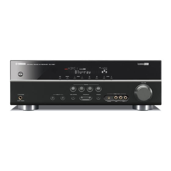
Page 3: Front Panels
RX-V367/HTR-3063 ■ FRONT PANELS Top view RX-V367 / HTR-3063 Front view RX-V367 (U, C, T models) RX-V367 (R, K, A, B, G, F, L models) - Page 4 RX-V367/HTR-3063 HTR-3063 (U, C, T models) HTR-3063 (R, K, A, G, F, L models)
-
Page 5: Rear Panels
RX-V367/HTR-3063 ■ REAR PANELS RX-V367 (U model) RX-V367 (C model) RX-V367 (R model) - Page 6 RX-V367/HTR-3063 RX-V367 (T model) RX-V367 (K model) RX-V367 (A model)
- Page 7 RX-V367/HTR-3063 RX-V367 (B, G, F models) RX-V367 (L model) HTR-3063 (U model)
- Page 8 RX-V367/HTR-3063 HTR-3063 (C model) HTR-3063 (R model) HTR-3063 (T model)
- Page 9 RX-V367/HTR-3063 HTR-3063 (K model) HTR-3063 (A model) HTR-3063 (G, E, F models)
- Page 10 RX-V367/HTR-3063 HTR-3063 (L model)
-
Page 11: Remote Control Panels
RX-V367/HTR-3063 ■ REMOTE CONTROL PANELS RAV331 RAV332 RAV333 (U, C models) (R, T, K, A, L models) (B, G, E, F models) Sheet (T model) -
Page 12: Specifications
RX-V367/HTR-3063 ■ SPECIFICATIONS ■ Audio Section Minimum RMS Output Power (Power Amp. Section) Residual Noise (IHF-A Network) (1 kHz, 0.9 % THD) FRONT L/R SP OUT ........150 μV or less U, C models (8 ohms) Channel Separation FRONT L/R ............100 W/ch AV5, etc. - Page 13 HDMI Licensing LLC. U, C, T, K, A, B, G, F models ......0.5 W or less R model ............1.0 W or less “SILENT CINEMA” is a trademark of Yamaha Corporation. Maximum Power Consumption ................... 440 W •...
- Page 14 RX-V367/HTR-3063 • SELECT MENU Sound field parameters Category Program MOVIE Standard ● ● Spectacle ● ● Sci-Fi ● ● Adventure ● ● Drama ● ● Mono Movie ● ● Sports ● ● Action Game ● ● Roleplaying Game ● ●...
- Page 15 RX-V367/HTR-3063 • SET MENU TABLE MAIN MENU SUB-MENU PARAMETER VALUE [INITIAL VALUE] 1 Speaker Setup 1 Config Subwoofer [Yes] / None Front speaker Small / [Large] Center speaker None / [Small] / Large Surround speaker L/R Crossover 40 / 60 / [80] / 90 / 100 / 110 / 120 / 160 / 200 Hz...
- Page 16 RX-V367/HTR-3063 MAIN MENU SUB-MENU PARAMETER VALUE [INITIAL VALUE] 4 DSP Parameter MOVIE Standard Spectacle Sci-Fi Adventure Drama [2], [9] Mono Movie Sports Action Game Roleplaying Game MUSIC Hall in Munich Hall in Vienna Chamber Cellar Club [2], [9] The Roxy Theatre...
-
Page 17: Internal View
RX-V367/HTR-3063 ■ INTERNAL VIEW OPERATION (3) P.C.B. MAIN (3) P.C.B. (R model) MAIN (1) P.C.B. AM/FM TUNER DIGITAL P.C.B. MAIN (2) P.C.B. OPERATION (4) P.C.B. MAIN (4) P.C.B. OPERATION (9) P.C.B. OPERATION (2) P.C.B. OPERATION (8) P.C.B. POWER TRANSFORMER OPERATION (7) P.C.B. -
Page 18: Disassembly Procedures
RX-V367/HTR-3063 ■ DISASSEMBLY PROCEDURES (Remove parts in the order as numbered.) Disconnect the power cable from the AC outlet. 1. Removal of Top Cover a. Remove 5 screws ( ① ) and 4 screws ( ② ). (Fig. 1) b. Slide the top cover rearward to remove it. (Fig. 1) 2. - Page 19 RX-V367/HTR-3063 3. Removal of DIGITAL P.C.B. a. Remove CB222–223 and CB262. (Fig. 2) b. Remove 2 screws (U, C models)/1 screw (R, T, K, A, B, G, L models) ( ④ ) and 5 screws ( ⑤ ). (Fig. 3) c.
- Page 20 RX-V367/HTR-3063 When checking the P.C.B. a. Remove the top cover. (Fig. 1) b. Remove 3 screws ( ⑧ ). (Fig. 3) c. Remove 5 screws ( ⑨ ) and 4 screws ( ⑩ ). (Fig. 4) d. Place the P.C.B.s (with rear panel) upright. (Fig. 5) e.
-
Page 21: Updating Firmware
RX-V367/HTR-3063 ■ UPDATING FIRMWARE Note) Updating the firmware restores all the set up information (soundfield parameters, system memory and tuner presetting, etc.) to the original factory settings. When the following parts are replaced, the firmware must be updated to the latest version. - Page 22 RX-V367/HTR-3063 ● Connection Connect this unit and DVD/CD player as shown below. (Fig. 1) Example of connection between digital OPTICAL jacks This unit DVD/CD player Optical cable Example of connection between digital COAXIAL jacks This unit DVD/CD player Digital audio pin cable...
-
Page 23: Rx-V367/Htr-3063 Operation Procedures
RX-V367/HTR-3063 ● Operation Procedures 1. While pressing the “INFO” key of this unit, connect the power cable of this unit to the AC outlet. (Fig. 2) The FIRMWARE UPDATE mode is activated and “CDDA Upgrader” is displayed. (Fig. 2) "INFO" key... - Page 24 RX-V367/HTR-3063 ■ SELF-DIAGNOSTIC FUNCTION This unit has self-diagnostic functions that are intended for inspection, measurement and location of faulty point. There are 26 main menu items, each of which has sub-menu items. Listed in the table below are main menu items and sub-menu items.
- Page 25 RX-V367/HTR-3063 Main menu Sub-menu HDMI INFORMATION 1 MODEL NAME 2 PRODUCT ID 3 VENDOR NAME HDMI SELECT 1 HDMI NONE 2 HDMI IN 1 * * 3 HDMI IN 2 * * 4 HDMI IN 3 * * 5 HDMI IN 4 * *...
-
Page 26: Starting/Canceling Self-Diagnostic Function
RX-V367/HTR-3063 ● Starting Self-Diagnostic Function While pressing the “TONE CONTROL” and “STRAIGHT” keys of this unit as shown in the figure below, press the “ ” (Power) key of this unit to turn on the power. The self-diagnostic function mode is activated. -
Page 27: Display Provided When Self-Diagnostic Function Started
RX-V367/HTR-3063 ● Display provided when Self-Diagnostic Function started The display is as described below depending on the situation when the last time the power to this unit is turned off. 1. When the power is turned off by usual operation: The FL display of this unit displays “NO PROTECT”... - Page 28 RX-V367/HTR-3063 2-2. When the protection function worked due to a short between speaker terminals. I P R O T E C T : x x x AD value when the protection function is working Cause: The line between speaker terminals is shorted.
- Page 29 RX-V367/HTR-3063 2-5. When the protection function worked due to excessive heatsink temperature. T H M P R T : x x x AD value when the protection function is working Cause: The temperature of the heatsink is excessive. Supplementary information: The protection function worked due to the temperature limit being exceeded.
- Page 30 RX-V367/HTR-3063 ● Operation procedure of Main menu and Sub-menu There are 26 main menu items, each of having sub-menu items. Main menu selection Select the menu using “SCENE TV” (forward) and “SCENE BD/DVD” (reverse) keys. Sub-menu selection Select the sub-menu using “SCENE RADIO” (forward) and “SCENE CD” (reverse) keys.
- Page 31 RX-V367/HTR-3063 ● Details of Self-Diagnostic Function menu 1. BYPASS Using the sub-menu, it is possible to select ANALOG BYPASS output. 1-1. ANALOG BYPASS The analog input audio signal is output to FRONT L/R in DIRECT mode. 1 . A N A L O G B Y P A S...
- Page 32 RX-V367/HTR-3063 2. RAM THROUGH Using the sub-menu, it is possible to select MARGIN output or FULL BIT output. 2-1. RAM MARGIN The audio signal is output including the head margin. 2 . R A M M A R G I N...
- Page 33 RX-V367/HTR-3063 2-4. RAM FULL SURROUND The audio signal is output to only SURROUND L/R channels in digital full bit without including the head margin. 2 . R A M F U L L S U R INPUT: AV5 ANALOG SPEAKER OUT: 1 kHz, SUBWOOFER OUTPUT: 50 Hz...
- Page 34 RX-V367/HTR-3063 3. HDMI AUDIO Using the sub-menu, the audio signals input to HDMI IN are selected and output. When selecting “DSD”, be sure to connect an HDMI unit equipped with DSD output function to this unit. 3-1. SPDIF 3 . S P D I F SPDIF signal is output.
- Page 35 RX-V367/HTR-3063 4-1. FRONT: SML 0dB 4 . F R N T : S M L 0 d B The FRONT L/R signal, when 90 Hz or lower, is mixed to the channel specified by LFE/BASS. 4-2. CENTER: NONE 4 . C E N T E R : N O N E The CENTER signal is distributed to FRONT L/R.
- Page 36 RX-V367/HTR-3063 5. LIMITER CONTROL Not for service. When “5-3. LIM/PLDET/THM” sub-menu is selected, keys become non-operable. However, it is possible to advance to the next main menu by pressing the “SCENE TV” (forward) or “SCENE BD/DVD” (reverse) keys of this unit.
- Page 37 RX-V367/HTR-3063 FL/MONITOR CHECK This menu is used to check the FL display and video monitor output. When checking the video monitor output, connect a TV monitor to this unit with a component video cable and video pin cable. Using the sub-menu, the FL display and video monitor output change together as shown below.
- Page 38 RX-V367/HTR-3063 8. MANUAL TEST The built-in noise generator of DSP outputs the test noise through the channels specified by using the sub-menu. The noise frequency for subwoofer is 30 to 80 Hz. Other than that, the noise frequency is 500 to 2 kHz.
- Page 39 RX-V367/HTR-3063 9-3. AMP/DK AMP: Power amplifier output is detected. Normal value: 128 to 255 (Reference voltage: 3.3 V=255) DOCK type detection (U, C models) (Reference voltage: 3.3 V=255) A M P : 2 5 5 D K : 2 5 5...
- Page 40 RX-V367/HTR-3063 10. VIDEO CHECK This menu is used to check the video control section. 10-1. I2C check The I2C (Inter integrated circuit) bus line connection is checked. 0 : No error detected I 2 C : 0 0 0 0 0 0 0 0 1 : An error is detected 0 bit : –...
- Page 41 RX-V367/HTR-3063 11. NO MENU 1 1 . I n v a l i d i t y 12. NO MENU 1 2 . I n v a l i d i t y 13. NO MENU 1 3 . I n v a l i d i t y...
- Page 42 RX-V367/HTR-3063 14. DOCK 14-1. DOCK This menu is used to check the DOCK connector without the iPod itself. With the power to this unit turned off, short between pins No. 14 (TX) and No. 18 (RX), between pins No. 4 (iPDET) and No.
- Page 43 15-3. HDMI vendor name V N : Y A M A H A The vendor name “YAMAHA” of this unit written in HDMI module is displayed. 16. HDMI SELECT Using the sub-menu, the selected input signal is output to HDMI OUT.
- Page 44 RX-V367/HTR-3063 17. NO MENU 1 7 . I n v a l i d i t y 18. IF STATUS (Input function status) Not for service. D S T : 7 1 0 E 0 F 2 3 9 0 19.
- Page 45 RX-V367/HTR-3063 21. PROTECTION HISTORY This menu is used to display the history of protection function. All history of protection function will be erased by pressing the “STRAIGHT” key. Example 21-1. History 1 2 1 - 1 . P S 1 0 7 8 L H: When the upper limit of the protection function is exceeded.
- Page 46 Press the “STRAIGHT” key is selected. 22-2. MODEL Press the “STRAIGHT” key to select the model name, “V367” (RX-V367) or “H3063” (HTR-3063). Selected model name is written. 2 2 . M O D E L : V 3 6 7 2 2 .
- Page 47 RX-V367/HTR-3063 23. UPDATE TI Not for service. 2 3 . U P D A T E T I 24. FACTORY PRESET This menu is used to reserve/inhibit initialization of the back-up IC (EEPROM: IC222 of the DIGITAL P.C.B.). 24-1. PRESET INHIBIT (Initialization inhibited) 2 4 .
- Page 48 DESTINATION detection value Detection value Destination B, G, F MODEL detection value Detection value Model name V3 (RX-V367) H3 (HTR-3063) 25-6. VERIFY V e r i f y 2 5 5 Not for service. 26. MODEL/DESTINATION Not for service. 2 6 . M O D E L / D E S T...
-
Page 49: Display Data
RX-V367/HTR-3063 ■ DISPLAY DATA ● V1001 : 18-MT-09GNK (OPERATION P.C.B.) PATTERN AREA ● PIN CONNECTION Pin No. 68 67 Connection F2 NX Pin No. 29 28 Connection Note : 1) F1, F2 ..Filament pin 2) NP ..No pin 3) NX .. - Page 50 RX-V367/HTR-3063 ● ANODE CONNECTION 1G-14G –...
- Page 51 RX-V367/HTR-3063 ■ IC DATA IC21: R2A15220FP (MAIN P.C.B.) 8-channel electronic volume with 11 input selector and tone control 49 48 46 45 38 37 34 33 TRER MUTE AVEE AVCC BASSR2 A VEE BASSR1 ADCL 0/-6/-12/-18dB TREL ADCR SUB2 BASSL2...
- Page 52 RX-V367/HTR-3063 Pin No. Port Name Function Name Detail of Function AGND Analog ground of internal circuit SBROUT VOSBL Output pin of FL/FR/C/SW/SL/SR/SBL/SBR channel SBR Pre-OUT VOPSBL Pre-output pin of FL/FR/SL/SR/SBL/SBR channel SBRC Connects capacitor for reducing click noise of L/R/C/SW/SL/SR/SBL/SBR channel volume...
- Page 53 RX-V367/HTR-3063 Pin No. Port Name Function Name Detail of Function MUTE Outside mute control pin AVEE – Negative power supply to internal circuit ADCL Output pin for L/R channel ADC ADCR AGND Analog ground of internal circuit INR1 AU2L INL1...
- Page 54 RX-V367/HTR-3063 IC241: D70YE101BRFP266 (DIGITAL P.C.B.) Decoder/Post processor * No replacement part available. SPI0_SIMO EM_CKE SPI0_SOMI/I2C0_SDA EM_CLK AXR0[0] EM_WE_DQM[1] AXR0[1] EM_D[8] AXR0[2] AXR0[3] EM_D[9] EM_D[10] AXR0[4] AXR0[5]/SPI1_SCS EM_D[11] AXR0[6]/SPI1_ENA AXR0[7]/SPI1_CLK EM_D[12] EM_D[13] EM_D[14] AXR0[8]/AXR1[5]/SPI1_SOMI EM_D[15] AXR0[9]/AXR1[4]/SPI1_SIMO EM_D[0] AXR0[10]/AXR1[3] EM_D[1] AXR0[11]/AXR1[2] EM_D[2]...
- Page 55 RX-V367/HTR-3063 Function Name TYPE PULL GPIO Detail of Function (P.C.B.) AHCLKX0/AHCLKX2 – McASP0 and McASP2 transmit master clock AMUTE0 – McASP0 mute output AMUTE1 – McASP1 mute output AHCLKX1 – McASP1 transmit master clock ACLKX1 – McASP1 transmit bit clock...
- Page 56 RX-V367/HTR-3063 Function Name TYPE PULL GPIO Detail of Function (P.C.B.) EM_D[1] – EMIF data bus [lower 16-bits] EM_D[0] – EMIF data bus [lower 16-bits] CVDD EM_D[15] – EMIF data bus [lower 16-bits] EM_D[14] – EMIF data bus [lower 16-Bits] CVDD EM_D[13] –...
- Page 57 RX-V367/HTR-3063 Function Name TYPE PULL GPIO Detail of Function (P.C.B.) 101 CVDD 102 NC – Asynchronous memory read/not write 103 DVDD 104 EM_OE – SDRAM output enable 105 SPI0_ENA/I2C1_SDA – SPI0 enable (ready) or I2c1 serial data 106 VSS 107 SPI0_ENA/I2C1_SCL –...
- Page 58 RX-V367/HTR-3063 IC221: R5F364AMNBF (DIGITAL P.C.B.) Microprocrssor Port P0 Port P1 Port P1 Port P3 Port P4 Port P5 VCC2 ports Internal peripheral functions System clock generator UART or clock synchronous serial I/O Timer (16-bit) XIN-XOUT (6 channels) XCIN-XCOUT Outputs (timer A): 5...
- Page 59 RX-V367/HTR-3063 Function P i n Port Name Name Full on Power off MCU sleep AC off Detail of Function (P.C.B.) RDS READY input / Open drain output (Imax=8 1 TB4IN RDS_RDY Low Fix Low Fix Low Fix mZ) on LC72725 side...
- Page 60 RX-V367/HTR-3063 Function P i n Port Name Name Full on Power off MCU sleep AC off Detail of Function (P.C.B.) 37 P5_7 N_DIR_RST DIR reset Low Act Low Fix Low Fix Low Fix 38 P5_6 N_DIR_CS DIR chip select Low Act...
- Page 61 RX-V367/HTR-3063 Function P i n Port Name Name Full on Power off MCU sleep AC off Detail of Function (P.C.B.) 66 N_INT6 N_DIR_INT DIR interrupt input Low Fix 67 P2_3 HPRY Headphone relay control High Act Low Fix Low Fix...
- Page 62 RX-V367/HTR-3063 Function P i n Port Name Name Full on Power off MCU sleep AC off Detail of Function (P.C.B.) 95 AN0 IPD_TYPE DOCK discriminate AD standby AD standby AD standby 96 VREF VREF AD reference voltage 97 AVCC AVCC...
- Page 63 RX-V367/HTR-3063 ■ BLOCK DIAGRAM DIGITAL → I2C2 SCHEMATIC DIAGRAM 29-32 HDMI IN 1 Port0 N_HRX_RST N_HTX_RST HDM_INT 33-36 IC201 IC202 HDMI IN 2 Port1 HDM_MUT Digital Video Data HDMI OUT HDMI RX HDMI Tx 37-40 HDMI IN 3 Port2 SiI9233...
- Page 64 RX-V367/HTR-3063 ■ PRINTED CIRCUIT BOARDS POINT C 1 / IC221 (97 pin, +3.3M), 2 / IC221 (10 pin, N_RESET) POINT D XL261 (Pin 29 of IC261) POINT A XL201 (Pin 5 of IC201) POINT B XL221 (Pin 11 of IC221) DIGITAL P.C.B.
- Page 65 RX-V367/HTR-3063 DIGITAL P.C.B. (Side B) U, C models B, G, F models • Semiconductor Location Ref no. Location D2201 IC266 D2203 D2204 IC203 D2607 IC242 D2610 IC203 IC242 IC266 IC268 Q2001 Q2002 Q2003 Q2004 Q2005 Q2006 Q2007 Q2008 Q2206...
- Page 66 RX-V367/HTR-3063 OPERATION (1) P.C.B. (Side A) DIGITAL (CB221) OPERATION (7) (CB171) DGND N_MIC_DET VOL_RB VOL_RA REM_IN PSW_DET N_FLD_RST FLD_SCK N_MIC_DET FLD_MOSI N_FLD_CS KEY2 KEY1 +3.3S DGND +3.3M AUX-V SW116 OPERATION (2) SW109 SW105 SW103 SW101 SW113 SW111 SW107 (CB136) TUNING...
- Page 67 RX-V367/HTR-3063 OPERATION (1) P.C.B. (Side B) • Semiconductor Location Ref no. Location Ref no. Location D1001 Q1002 D1002 Q1003 D1003 Q1004 D1004 Q1005 D1005 Q1006 D1006 Q1007 IC101 Q1008 Q1001...
- Page 68 RX-V367/HTR-3063 OPERATION (2) P.C.B. (Side A) C model U, C models OUT COM IN OUT COM IN OUT COM IN OUT COM IN IC132 IC135 IC133 IC134 IC131 U, C models OPERATION (1) (CB102) CB131 CB132 DIGITAL (CB262) POWER TRANSFORMER MAIN (1) OPERATION (3) P.C.B.
- Page 69 RX-V367/HTR-3063 OPERATION (2) P.C.B. (Side B) U, C models R, T, K, A, B, G, L models U, C models U, C models OPERATION (3) P.C.B. (Side B) • Semiconductor Location Ref no. Location D1301 D1302 D1303 D1305 D1306 D1311...
- Page 70 RX-V367/HTR-3063 OPERATION (4) P.C.B. OPERATION (5) P.C.B. (Side A) (Side A) PHONES MAIN (1) SILENT CINEMA MAIN (1) (CB22) (CB21) CB192 CB191 JK166 MAIN (1) (W1) N_HP_DET -12V OPERATION (6) P.C.B. (Side A) AGND CB194 +12V VAUX VAUXE AUXL AUXE...
- Page 71 RX-V367/HTR-3063 OPERATION (4) P.C.B. OPERATION (5) P.C.B. (Side B) (Side B) OPERATION (6) P.C.B. (Side B) • Semiconductor Location Ref no. Location D1651 D1652 D1653...
- Page 72 RX-V367/HTR-3063 OPERATION (7) P.C.B. OPERATION (8) P.C.B. (Side A) (Side A) R, K, A, B, G, L models N_MIC_DET OPERATION (1) (CB103) JK171 SW171 YPAO MIC OPERATION (9) P.C.B. (Side A)
- Page 73 RX-V367/HTR-3063 OPERATION (7) P.C.B. OPERATION (8) P.C.B. (Side B) (Side B) R, K, A, B, G, L models • Semiconductor Location Ref no. Location D1701 D1702 D1703 IC102 OPERATION (9) P.C.B. (Side B)
- Page 74 RX-V367/HTR-3063 SPEAKERS FRONT MAIN (1) P.C.B. SURROUND CENTER (Side A) AV 1 AV 2 AV 3 AV 4 AV 5 AV OUT AUDIO1 AUDIO2 AUDIO SUBWOOFER OPTICAL COAXIAL COAXIAL OPTICAL (TV) (CD) PJ21 PJ24 PJ22 PJ26 OPERATION (4) (CB192) AV1_D...
- Page 75 RX-V367/HTR-3063 MAIN (1) P.C.B. (Side B) IC22 IC23 IC25 IC24 IC27 • Semiconductor Location Ref no. Location Ref no. Location IC21 IC22 Q201 IC23 Q202 IC24 Q203 IC25 Q204 IC27 Q205 Q208 Q209...
- Page 76 RX-V367/HTR-3063 MAIN (2) P.C.B. MAIN (3) P.C.B. (Side A) (Side A) R model MONITOR OUT AV 4 AV 5 MONITOR COMPONENT COMPONENT VIDEO VIDEO VIDEO PJ43 PJ44 PJ42 PJ45 PJ41 SW51 CB51 VOLTAGE SELECTOR 220V 240V 110V 120V POWER TRANSFORMER N_CPNT_MT •...
- Page 77 RX-V367/HTR-3063 MAIN (2) P.C.B. MAIN (3) P.C.B. (Side B) (Side B) R model IC42 IC43 IC41 • Semiconductor Location Ref no. Location D401 IC41 IC42 MAIN (4) P.C.B. (Side B) IC43...
- Page 78 RX-V367/HTR-3063 ■ PIN CONNECTION DIAGRAMS • ICs • Diodes BD9325FJ D70YE101BRFP266 KIA7805API KIA7812API KIA7912PI 1N4003S 1SS355 HZU3.3B2 TRF-E SiI9233ACTU 1SS133 1SS176 Anode Anode Anode 1SS270A Anode Cathode Cathode Cathode Cathode KBP103G 1.0A 200V KDS160-RTK MTZJ4.7A RB051LA-40 MTZJ6.8C RB501V-40 MTZJ10B Anode...
- Page 79 RX-V367/HTR-3063 SCHEMATIC DIAGRAMS DIGITAL 1/4 HDMI 4 HDMI 3 HDMI 2 HDMI 1 HDMI OUT (BD/DVD) CB204 CB203 CB202 CB201 CB205 IC204 IC204 IC204 IC204 To DIGITAL 4/4 To DIGITAL 2/4 HDMI RX HDMI TX IC201 IC202 No replacement part available.
- Page 80 RX-V367/HTR-3063 DIGITAL 2/4 Page 83 Page 85 To AM/FM TUNER to OPERATION (1)_CB101 to MAIN (1)_CB1 CB221 CB222 CB223 (B, G, F models) IC223 To DIGITAL 4/4 -11.7 -11.7 -11.7 IC221: R5F364AMNFB Single chip 16-bit microprocessor MICROPROCESSOR Port P0 Port P1...
- Page 81 RX-V367/HTR-3063 DIGITAL 3/4 DIGITAL IN To DIGITAL 4/4 To DIGITAL 1/4 To DIGITAL 4/4 FL/FR SL/SR C/SW AUDIO DSP IC241 IC246 To DIGITAL 2/4 No replacement part available. サービス部品供給なし CB241 IC243: MX29LV160DBTI-70G 16M-bit 3V supply flash memory IC242: M12L64164A-5TG IC241:...
- Page 82 RX-V367/HTR-3063 DIGITAL 4/4 No replacement part available. IC261: LC89058WD-E Digital audio interface receiver DOCK DIGITAL IN サービス部品供給なし MOUT AUDIO CB261 XMODE Fs calculator GPIO0 Microprocessor 40 CL GPIO1 GPIO2 Cbit, Pc GPIO3 RXOUT2 RXOUT1 Input RERR Demodulation Selector SDIN Lock detect...
- Page 83 RX-V367/HTR-3063 OPERATION 1/2 -31.9 -31.9 -31.8 -31.8 -34.0 -36.2 -29.8 -36.2 -31.9 -34.0 -34.0 -31.9 -38.3 -34.0 -36.2 -31.9 OPERATION (5) -29.8 -34.0 -34.0 IC101: M66003-0131FP-R IC101 18 digit 5 x 7 segment VFD controller/driver -34.0 -31.9 -29.1 CB102 -36.2 JK166 -34.2...
- Page 84 RX-V367/HTR-3063 OPERATION 2/2 Page 83 to OPERATION (1)_CB104 CB193 CB191 -11.8 12.1 -11.7 -11.7 -11.7 -11.7 -11.7 -11.7 Page 86 Page 82 to MAIN (1)_CB22 to DIGITAL_CB264 SURROUND L SUBWOOFER CENTER CB195 FRONT L CB192 Page 86 to MAIN (1)_CB21...
-
Page 85: 3-Channel Af Power Amplifier/Stand-By Circuit Built-In
RX-V367/HTR-3063 MAIN 1/3 MAIN (1) 54.2 54.1 FRONT SPEAKERS FRONT L 53.8 Page 80 to DIGITAL_CB222 IC1: STK433-330Y-E 3-channel AF power amplifier, stand-by circuit built-in -11.7 To MAIN 2/3 Driver Driver Driver MONO IC – – – 53.8 Bias Circuit... - Page 86 RX-V367/HTR-3063 MAIN 2/3 Page 84 Page 84 to OPERATION (4)_CB192 to OPERATION (4)_CB191 IC21: R2A15220FP 8-channel electronic volume with 11 input selector and tone control MAIN (1) 49 48 46 45 38 37 34 33 TRER MUTE AVEE AVCC A VEE...
- Page 87 RX-V367/HTR-3063 MAIN 3/3 Page 84 MAIN (2) to OPERATION (4)_CB194 MONITOR COMPONENT VIDEO IC41: NJM2586AM (TE2) Wide band 3-input 1-output 3-circuit video amplifier CH1 IN1 CH1 OUT Driver Bias Cont1 SW 1 Cont1 Cont2 CH1 IN2 CH2 OUT Driver Bias...
-
Page 88: Replacement Parts List
RX-V367/HTR-3063 ■ REPLACEMENT PARTS LIST • ELECTRICAL COMPONENT PARTS WARNING ● Components having special characteristics are marked and must be replaced with parts having specifications equal to those originally installed. ABBREVIATIONS IN THIS LIST ARE AS FOLLOWS: C.A.EL.CHP : CHIP ALUMI.ELECTROLYTIC CAP L.EMIT... - Page 89 RX-V367/HTR-3063 P.C.B. DIGITAL P.C.B. DIGITAL Ref No. Part No. Description Markets Ref No. Part No. Description Markets WU125000 P.C.B. DIGITAL C2264-2265 US061270 C.CE.CHP 27pF 50V B WU125100 P.C.B. DIGITAL RTKAL C2266 UR867100 C.EL 10uF WU125200 P.C.B. DIGITAL C2267 US126100 C.CE.CHP CB201-205 WU167400 CN.HDMI...
- Page 90 RX-V367/HTR-3063 P.C.B. DIGITAL and P.C.B. OPERATION P.C.B. OPERATION Ref No. Part No. Description Markets Ref No. Part No. Description Markets C2701-2707 US135100 C.CE.CHP 0.1uF C1015 US135100 C.CE.CHP 0.1uF D2022 VV220700 DIODE.SCHOTTKY RB501V-40 C1016 US061680 C.CE.CHP 68pF 50V B * D2201-2204 WS692300 DIODE.ZENR HZU3.3B2 TRF-E C1017 US065100 C.CE.CHP...
- Page 91 RX-V367/HTR-3063 P.C.B. OPERATION P.C.B. MAIN Ref No. Part No. Description Markets Ref No. Part No. Description Markets D1308-1309 WA653100 DIODE.BRG KBP103G 1A 200V WU124200 P.C.B. MAIN UCTA D1311-1312 VT332900 DIODE 1SS355 WU124300 P.C.B. MAIN D1313-1314 VT332900 DIODE 1SS355 WU124400 P.C.B.
-
Page 92: P.c.b. Main Parts
RX-V367/HTR-3063 P.C.B. MAIN P.C.B. MAIN Ref No. Part No. Description Markets Ref No. Part No. Description Markets C239-243 US062680 C.CE.CHP 680pF 50V B X7427B00 IC STK433-130Y-E C244 WJ605800 C.MYLAR 0.047uF 50V J * IC21 YA361A00 IC R2A15220FP C247-249 US062100 C.CE.CHP... - Page 93 RX-V367/HTR-3063 P.C.B. MAIN Ref No. Part No. Description Markets Ref No. Part No. Description Markets R433 HV753100 R.CAR.FP 1Ω 1/4W RY1-4 WJ122400 RELAY 981-2A-24DS-SP7 WE648700 RELAY DC DH24D2-O-Q WK560800 TERM.SP 4P MST-204V1-01 NC UCRTA WK560900 TERM.SP 4P MST-204V1-01 WC KBGFL WB214000 TERM.SP...
- Page 94 RX-V367/HTR-3063 Carbon Resistors Value 1/4W Type Part No. 1/6W Type Part No. Value 1/4W Type Part No. 1/6W Type Part No. 1.0 Ω HJ35 3100 HF85 3100 11 kΩ HF45 7110 HF45 7110 ✻ 1.8 Ω 3180 12 kΩ 7120...
- Page 95 RX-V367/HTR-3063 • OVERALL ASS'Y L model 200-1 R model U, C, R, T, L models 2-1 (3) K, A, B, G, F models T model 1-1 (2) 2-104 2-104 2-1 (2) 1-1 (7) 1-1 (4) 1-25 1-1 (3) 1-25 2-104...
- Page 96 RX-V367/HTR-3063 Ref No. Part No. Description Remarks Markets Ref No. Part No. Description Remarks Markets * 1-1 WU124500 P.C.B. ASS'Y OPERATION * 103 WT826300 REAR PANEL 3063 * 1-1 WU124600 P.C.B. ASS'Y OPERATION * 103 WT825600 REAR PANEL V367 * 1-1 WU124700 P.C.B.
- Page 97 RX-V367/HTR-3063 ■ REMOTE CONTROL ● RAV331: U, C models / RAV332: R, T, K, A, L models / RAV333: B, G, F models SCHEMATIC DIAGRAMS PANELS RAV331, RAV332 RAV331 RAV332 RAV333 (U, C models) (R, T, K, A, L models)
- Page 98 RX-V367/HTR-3063 KEY NO. LAYOUT KEY CODE RAV331, RAV332 RAV331, RAV332 AMP MODE FUNCTION FUNCTION GROUP GROUP (U, C, R, K, A, L models) (T model) MAIN (ZONE2) (ZONE3) MAIN (ZONE2) (ZONE3) (U, C, R, K, A, L models) (T model)
- Page 99 RX-V367/HTR-3063 RAV331, RAV332 RAV331, RAV332 SOURCE MODE SOURCE MODE 1 (INPUT1) SOURCE MODE 2 (INPUT2) [HDMI-1] [HDMI-2] [HDMI-3] [HDMI-4] [AV-1] [AV-2] [AV-3] [AV-4] [AV-5] [AUDIO-1] [AUDIO-1] [V-AUX] [DOCK] [TUNER] FUNCTION GROUP (U, C, R, K, A, L models) (T model)
- Page 100 RX-V367/HTR-3063 RAV331, RAV332 RAV331, RAV332 SOURCE MODE SOURCE MODE 1 (INPUT1) SOURCE MODE 2 (INPUT2) [HDMI-1] [HDMI-2] [HDMI-3] [HDMI-4] [AV-1] [AV-2] [AV-3] [AV-4] [AV-5] [AUDIO-1] [AUDIO-1] [V-AUX] [DOCK] [TUNER] FUNCTION GROUP (U, C, R, K, A, L models) (T model)
- Page 101 RX-V367/HTR-3063 KEY NO. LAYOUT KEY CODE RAV333 RAV333 CODE Key No. FUNCTION MAIN ZONE2 ZONE3 MAIN ZONE2 ZONE3 SLEEP 7A-30 7A-31 7A-32 7A-30CE 7A-31CF 7A-32CC 7E-2A 7A-453A 7A-4639 7E-2AD4 7A-453B 7A-4638 HDMI-1 7A-4738 7A-4837 7A-4936 7A-4739 7A-4836 7A-4937 HDMI-2 7A-4A35...
- Page 102 RX-V367/HTR-3063 ■ ADVANCED SETUP U, C models...
- Page 103 RX-V367/HTR-3063 R, T, K, A, B, G, F, L models (R, T, K, A, L models) (B, G, F models) (R, T, K, A, L models) (R, T, K, L models)
- Page 104 RX-V367/HTR-3063 MEMO...
- Page 105 RX-V367/HTR-3063...