Sony HT-XT100 Service Manual
Hide thumbs
Also See for HT-XT100:
- Operating instructions manual (79 pages) ,
- Startup manual (2 pages) ,
- Operating instructions manual (28 pages)
Table of Contents
Advertisement
SERVICE MANUAL
Ver. 1.0 2015.02
Note:
Be sure to keep your PC used for service and
checking of this unit always updated with the
latest version of your anti-virus software.
In case a virus affected unit was found during
service, contact your Service Headquarters.
Amplifier section
U.S. models:
POWER OUTPUT AND TOTAL HARMONIC
DISTORTION:
(FTC)
Front L + Front R:
With 4 ohms loads, both channels
driven, from 200 Hz - 20,000 Hz; rated
10 Watts per channel minimum RMS
power, with no more than 1% total
harmonic distortion from
250 milliwatts to rated output.
POWER OUTPUT (reference):
Front L/Front R speaker:
20 Watts (per channel at 4 ohms,
1 kHz)
Subwoofer:
40 Watts (at 4 ohms, 100 Hz)
Except US models:
POWER OUTPUT (rated)
Front L + Front R:
10 W + 10 W (at 4 ohms, 1 kHz, 1% THD)
POWER OUTPUT (reference)
Front L/Front R speaker:
20 Watts (per channel at 4 ohms,
1 kHz)
Subwoofer:
40 Watts (at 4 ohms, 100 Hz)
Inputs
ANALOG IN
DIGITAL IN
Output
HDMI OUT ARC
HDMI Section
Connector
Type A (19pin)
USB Section
(USB) port
Type A
9-896-125-01
Sony Corporation
2015B33-1
©
2015.02
Published by Sony Techno Create Corporation
HT-XT100
SPECIFICATIONS
BLUETOOTH section
Communication system
BLUETOOTH Specification version 4.0
Output
BLUETOOTH Specification Power Class
2
Maximum communication range
1)
Line of sight approx. 10 m (33 ft)
Maximum number of devices to be
registered
8 devices
Frequency band
2.4 GHz band (2.4000 GHz -
2.4835 GHz)
Modulation method
FHSS (Freq Hopping Spread Spectrum)
2)
Compatible BLUETOOTH profiles
A2DP (Advanced Audio Distribution
Profile)
AVRCP (Audio Video Remote Control
Profile)
3)
Supported Codecs
4)
SBC
Transmission range (A2DP)
20 Hz - 20,000 Hz (Sampling frequency
44.1 kHz)
1)
The actual range will vary depending on
factors such as obstacles between
devices, magnetic fields around a
microwave oven, static electricity,
cordless phone, reception sensitivity,
operating system, software application,
etc.
2)
BLUETOOTH standard profiles indicate
the purpose of BLUETOOTH
communication between devices.
3)
Codec: Audio signal compression and
conversion format
4)
Subband Codec
US Model
Canadian Model
AEP Model
UK Model
Australian Model
Speakers
Front L/Front R speaker section
Speaker system
2-way speaker system, Acoustic
suspension
Speaker
Tweeter: 14 mm - 25 mm (
balance dome type
Woofer: 43 mm × 120 mm (1
3
4
/
in) cone type
4
Subwoofer section
Speaker system
Subwoofer system
Bass reflex
Speaker
100 mm (4 in) cone type
General
Power requirements
120 V AC, 60 Hz (US and Canadian models)
220 V - 240 V AC, 50 Hz/60 Hz
(AEP, UK and Australian models)
Power consumption
On: 25 W
Standby mode (Control for HDMI is set
to on): 6 W or less
Standby mode (Control for HDMI is set
to off): 0.5 W or less
BLUETOOTH Standby mode: 6 W or
less
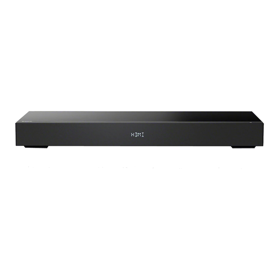
Dimensions (approx.) (w/h/d)
702 mm × 79 mm × 311 mm
3
1
(27
/
in × 3
/
in × 12
4
8
Mass (approx.)
6.5 kg (14 Ib 6 oz)
Supplied accessories
Remote control (1)
R03 (size AAA) batteries (2)
Optical digital cable (1)
Design and specifications are subject to
change without notice.
HOME THEATRE SYSTEM
9
/
in - 1 in)
16
3
/
in ×
4
1
/
in)
4
Advertisement
Table of Contents

Related Manuals for Sony HT-XT100


Summary of Contents for Sony HT-XT100
-
Page 1: Specifications
R03 (size AAA) batteries (2) USB Section Optical digital cable (1) Subband Codec (USB) port Design and specifications are subject to Type A change without notice. HOME THEATRE SYSTEM 9-896-125-01 Sony Corporation 2015B33-1 © 2015.02 Published by Sony Techno Create Corporation... - Page 2 LES DIAGRAMMES SCHÉMATIQUES ET LA LISTE DES PIÈCES SONT CRITIQUES POUR LA SÉCURITÉ DE FONC- TIONNEMENT. NE REMPLACER CES COMPOSANTS QUE PAR DES PIÈCES SONY DONT LES NUMÉROS SONT DON- NÉS DANS CE MANUEL OU DANS LES SUPPLÉMENTS PUBLIÉS PAR SONY.
-
Page 3: Table Of Contents
HT-XT100 TABLE OF CONTENTS SERVICING NOTES 4-3. Schematic Diagram - MAIN Board (1/6) - ..... 22 ..........4-4. Schematic Diagram - MAIN Board (2/6) - ..... 23 4-5. Schematic Diagram - MAIN Board (3/6) - ..... 24 DISASSEMBLY 4-6. Schematic Diagram - MAIN Board (4/6) - ..... 25 2-1. -
Page 4: Servicing Notes
HT-XT100 SECTION 1 SERVICING NOTES The SERVICING NOTES contains important information for servicing. Be sure to read this section before repairing the unit. UNLEADED SOLDER MODEL IDENTIFICATION Boards requiring use of unleaded solder are printed with the lead- Distinguish by model number label stuck on the rear side of a main free mark (LF) indicating the solder contains no lead. - Page 5 HT-XT100 ABOUT PARTS REPAIR OF EACH BOARDS When each boards installed in this unit are defective, individual electrical parts that the mount is done cannot be replaced. When each boards are defective, replace the mounted board or the whole parts including an applicable board.
-
Page 6: Disassembly
HT-XT100 SECTION 2 DISASSEMBLY • This set can be disassembled in the order shown below. 2-1. DISASSEMBLY FLOW 2-2. BOTTOM PANEL 2-8. LOUDSPEAKER (10 cm) (SP1) (Page 7) (Page 10) 2-3. BT NFC BOARD 2-4. AMP BLOCK (Page 7) (Page 8) 2-5. -
Page 7: Bottom Panel
HT-XT100 Note: Follow the disassembly procedure in the numerical order given. 2-2. BOTTOM PANEL 2 seven screws (3.5 12 B) 3 bottom panel 1 two screws 8 B2) – Rear bottom view – 2-3. BT NFC BOARD Note: When replacing the BT NFC board or the NFC module, be sure replace both at the same time. -
Page 8: Amp Block
HT-XT100 2-4. AMP BLOCK How to install the connector Insert the connector straight into the interior. There is a possibility that using this unit without 7 Remove wires POWER board hook the connector correctly installed will damage it. from the hook. -
Page 9: Power Cord (Ac1)
HT-XT100 2-5. POWER CORD (AC1) printing face white line power cord (AC1) power cord (AC1) POWER board POWER board 3 power cord (AC1) 1 connector (CN501) 2 Remove the power cord (AC1) in the direction of the arrow. – –... -
Page 10: Main Board
HT-XT100 2-7. MAIN BOARD 5 MAIN board 4 four screws 7 S) MAIN board POWER board 3 screw 1 connector 6 B) (XS1) 2 screw 10 B) hook – AMP block front bottom view – 2-8. LOUDSPEAKER (10 cm) (SP1) -
Page 11: Grille Assy
HT-XT100 2-9. GRILLE ASSY 1 While firmly pushing both ends of the grille assy with fingers, 1 While firmly pushing both ends wiggle it up and down to detach of the grille assy with fingers, the claws. wiggle it up and down to detach the claws. -
Page 12: Front Panel Block
HT-XT100 2-10. FRONT PANEL BLOCK How to install the connector Insert the connector straight into the interior. There is a possibility that using this unit without 3 FFC 16P/MAIN-FRONT (FFC2) 2 connector the connector correctly installed will damage it. (XP6) -
Page 13: Loudspeaker (4.3 × 12 Cm) (Sp2, Sp3)
HT-XT100 2-11. LOUDSPEAKER (4.3 × 12 cm) (SP2, SP3) loudspeaker (4.3 12 cm) (SP3) 1 terminal hook – Rear view – (narrow side) [black] 1 terminal (wide side) [white] [white] [black] groove (wide side) (narrow side) top side 1 terminal... -
Page 14: Loudspeaker (1.4 × 2.5 Cm) (Sp4, Sp5)
HT-XT100 2-12. LOUDSPEAKER (1.4 × 2.5 cm) (SP4, SP5) loudspeaker 1 terminal 1 terminal loudspeaker (narrow side) (4.3 12 cm) (wide side) (1.4 2.5 cm) [red] (SP3) [black] (SP5) screw hole – Rear view – 2 screw (2.6 8 S) 3 loudspeaker (1.4... -
Page 15: Key Board
HT-XT100 2-13. KEY BOARD 1 two screws (2.6 8 S) 8 button 7 two claws 5 KEY board block 2 Lift up the KEY board block 9 KEY board in the direction of the arrow. terminal side 6 two screws 4 FFC 8P/FRONT-KEY (FFC3) (2.6... -
Page 16: Nfc Module
HT-XT100 2-14. NFC MODULE Note: When replacing the BT NFC board or the NFC module, be sure replace both at the same time. The BT NFC board or the NFC module cannot replace with single. 1 Peel off the adhesive sheet. -
Page 17: Test Mode
HT-XT100 SECTION 3 TEST MODE VERSION DISPLAY DEMO MODE The check of the software version can be performed. The demo mode can be performed. (This mode is used by shop front) Note: At the same time it is cannot perform the hotel mode (page 18). - Page 18 HT-XT100 HOTEL MODE Initial setting for hotel mode: The hotel mode can be performed. When the power is turned on, always volume is “0”. (This mode is used by hotel equipment administrator) Maximum volume will be changed to the settings value (default Note: At the same time it is cannot perform the demo mode (page 17).
-
Page 19: Diagrams
HT-XT100 SECTION 4 DIAGRAMS 4-1. BLOCK DIAGRAM Audio signal SDRAM FLASH Control signal Control signal 20W *2 THD 30% I/O*4 74LVC2G04 HDMI OUT HDMI_ARC Power Stage I2C/RST/MUTE/FAULT STA339BW MTK 8301 Swith IC 40W THD 30% AK5358 AK5358 AUDIO IN 74LVC1G3157... - Page 20 HT-XT100 THIS NOTE IS COMMON FOR PRINTED WIRING BOARDS AND SCHEMATIC DIAGRAMS. • Circuit Boards Location (In addition to this, the necessary note is printed in each block.) For Printed Wiring Boards. For Schematic Diagrams. POWER board Note: Note: • All capacitors are in μF unless otherwise noted. (p: pF) 50 •...
-
Page 21: Printed Wiring Board - Main Board
HT-XT100 4-2. PRINTED WIRING BOARD - MAIN Board - • See page 20 for Circuit Boards Location. • : Uses unleaded solder. MAIN BOARD (COMPONENT SIDE) MAIN BOARD (CONDUCTOR SIDE) HT-XT100... -
Page 22: Schematic Diagram - Main Board (1/6)
HT-XT100 4-3. SCHEMATIC DIAGRAM - MAIN Board (1/6) - • See page 33 for IC Block Diagrams. • See page 36 for IC Pin Function Description. MAIN BOARD (1/6) D_3V3 C183 C183 10PF/50V/NP0 10PF/50V/NP0 C184 C184 10PF/50V/NP0 10PF/50V/NP0 A_1V2 300/2A... -
Page 23: Schematic Diagram - Main Board (2/6)
HT-XT100 4-4. SCHEMATIC DIAGRAM - MAIN Board (2/6) - • See page 36 for IC Pin Function Description. MAIN BOARD (2/6) +3.3VD +3.3VD1 +3.3VD1 FB25 FB25 500/200mA 500/200mA R167 R167 4.7K 4.7K 339_VCC C151 C151 VDD_DIG GND_SUB 0.1uF 0.1uF GND_DIG... -
Page 24: Schematic Diagram - Main Board (3/6)
HT-XT100 4-5. SCHEMATIC DIAGRAM - MAIN Board (3/6) - • See page 36 for IC Pin Function Description. MAIN BOARD (3/6) SYS_3V3 +3.3VD FB16 FB16 500/200mA 500/200mA C115 C115 0.1uF 0.1uF CE17 CE17 AMP_VCC 100uF/16V 100uF/16V I2C ADRESS 0*38 FB17... -
Page 25: Schematic Diagram - Main Board (4/6)
HT-XT100 4-6. SCHEMATIC DIAGRAM - MAIN Board (4/6) - • See page 33 for IC Block Diagrams. MAIN BOARD (4/6) R250 R250 NC/0 NC/0 POWER_18V 300/2A 300/2A POWER_18V AP4435GM AP4435GM AMP_VCC 6PIN/2.0mm 6PIN/2.0mm 220uF/35V 220uF/35V STB_5V 220uF/35V 220uF/35V 330pF/16V/NP0 330pF/16V/NP0... -
Page 26: Schematic Diagram - Main Board (5/6)
HT-XT100 4-7. SCHEMATIC DIAGRAM - MAIN Board (5/6) - • See page 33 for IC Block Diagrams. MAIN BOARD (5/6) CONNECT FE BD C801 C801 XP15 XP15 FB24 FB24 500/200mA 500/200mA R337 10K R337 10K MP3_R FB26 FB26 75/1A 75/1A SYS_5V 4.7UF/10V/X5R... -
Page 27: 4-8. Schematic Diagram - Main Board (6/6)
HT-XT100 4-8. SCHEMATIC DIAGRAM - MAIN Board (6/6) - MAIN BOARD (6/6) NC/ACM2012H-900-2P NC/ACM2012H-900-2P TX2+ TX2+ TX2- TX2- NC/ACM2012H-900-2P NC/ACM2012H-900-2P TX1+ TX1+ STB_5V HDMI_5V TX1- TX1- FB21 FB21 HDMI_5V NC/ACM2012H-900-2P NC/ACM2012H-900-2P TX0+ TX0+ MBRX120/20V/1A MBRX120/20V/1A TX0- HDMI_CEC TX0- HDMI_ARC R187... -
Page 28: Printed Wiring Board - Bt Nfc Board
HT-XT100 4-9. PRINTED WIRING BOARD - BT NFC Board - 4-10. SCHEMATIC DIAGRAM - BT NFC Board - • See page 20 for Circuit Boards Location. • : Uses unleaded solder. BT NFC BOARD BT NFC BOARD BT NFC BOARD... -
Page 29: Printed Wiring Board - Usb Board
HT-XT100 4-11. PRINTED WIRING BOARD - USB Board - 4-13. PRINTED WIRING BOARD - KEY Board - • See page 20 for Circuit Boards Location. • : Uses unleaded solder. • See page 20 for Circuit Boards Location. • : Uses unleaded solder. -
Page 30: Printed Wiring Board - Front Board
HT-XT100 4-15. PRINTED WIRING BOARD - FRONT Board - • See page 20 for Circuit Boards Location. • : Uses unleaded solder. FRONT BOARD (COMPONENT SIDE) FRONT BOARD (CONDUCTOR SIDE) HT-XT100... -
Page 31: Schematic Diagram - Front Board
HT-XT100 4-16. SCHEMATIC DIAGRAM - FRONT Board - • See page 33 for IC Block Diagrams. FRONT BOARD STB_3V3 BT_PAIR VOL- VOL+ STB_3V3 KEY_POWER KEY_SOURCE NFC_INT 0.1uF 0.1uF XP15 XP15 R225 R225 8PIN/1.0mm 8PIN/1.0mm 4.7K 4.7K NFC_INT R244 R244 BT_STATUS 4.7K... -
Page 32: Printed Wiring Board - Power Board
HT-XT100 4-17. PRINTED WIRING BOARD - POWER Board - 4-18. SCHEMATIC DIAGRAM - POWER Board - • See page 20 for Circuit Boards Location. • : Uses unleaded solder. POWER BOARD POWER BOARD POWER BOARD (COMPONENT SIDE) (CONDUCTOR SIDE) TR501... - Page 33 HT-XT100 • IC Block Diagrams – MAIN Board – U2, 3 EUP3482A U4 LD1117STR U5, 6 74LVC1G3157GV U8 AK5358A AGND DGND MCLK Clock Divider Decimation AINL Modulator Filter LRCK SCLK Decimation AINR Modulator Filter Serial I/O SDTO Interface VCOM Voltage Reference...
- Page 34 HT-XT100 U10 M12L64164A-7T Clock Generator Bank D Bank C Bank B Address Address Buffer Mode Bank A & Register Refresh Counter Sense Amplifier L(U)DQM Column Column Decoder Address Buffer & Refresh Counter Data Control Circuit U14 G527 Output Reverse-Voltage Output Reverse-Voltage...
- Page 35 HT-XT100 – FRONT Board – IR1 HRM140BB7801C CGA & fliter Input Demodulator Oscillator AGC / ATC & digital control U1 ET6240...
- Page 36 HT-XT100 • IC Pin Function Description MAIN BOARD U11 MTK8301OXE (SYSTEM CONTROLLER) Pin No. Pin Name Description AVDD12_2 Power supply terminal (+1.2V) AVDD33_1 Power supply terminal (+3.3V) XTALI System clock input terminal (27 MHz) XTALO System clock output terminal (27 MHz) Reference voltage (+1.4V) input terminal...
- Page 37 HT-XT100 Pin No. Pin Name Description 77 to 81 RA10, RA0 to RA3 Address signal output terminal (for SDRAM) DVDD12 Power supply terminal (+1.2V) SPDIF/GPIO12 Interrupt request signal input terminal (for NFC) GPIO10/HPLG Hot plug detection signal input terminal (for HDMI)
- Page 38 HT-XT100 MAIN BOARD U13 STA339BW (DIGITAL AMP) Pin No. Pin Name Description GND_SUB Ground terminal I2C select address signal input terminal Fixed at “L” in this unit TEST_MODE Fixed at “L” in this unit Internal reference voltage (–3.3V) input/output terminal...
- Page 39 HT-XT100 MAIN BOARD U15 STA369BWS (DIGITAL AMP) Pin No. Pin Name Description GND_SUB Ground terminal I2C select address signal input terminal Fixed at “H” in this unit TEST_MODE Fixed at “L” in this unit Internal reference voltage (–3.3V) input/output terminal...
-
Page 40: Exploded Views
HT-XT100 SECTION 5 EXPLODED VIEWS Note: • -XX and -X mean standardized parts, so • The mechanical parts with no reference The components identifi ed by mark 0 they may have some difference from the number in the exploded views are not sup- or dotted line with mark 0 are critical for original one. -
Page 41: Front Panel Section
HT-XT100 5-2. FRONT PANEL SECTION not supplied not supplied not supplied not supplied FFC2 56 56 included in Ref. No. 10 on page 40 NFC module (See Note) FFC3 58 59 53 53 Note: When replacing the BT NFC board or the NFC module, be sure replace both at the same time. -
Page 42: Accessories
HT-XT100 SECTION 6 ACCESSORIES Ref. No. Part No. Description Remark 4-559-030-11 MANUAL, INSTRUCTION (ENGLISH, FRENCH, SPANISH) (US, CND) 4-559-030-21 MANUAL, INSTRUCTION (ENGLISH) (UK, AUS) 4-559-030-31 MANUAL, INSTRUCTION (FRENCH, SPANISH, DUTCH) (AEP) 4-559-030-41 MANUAL, INSTRUCTION (GERMAN, POLISH, ITALIAN) (AEP) 4-569-354-11 MANUAL, INSTRUCTION (SWEDISH) (AEP) - Page 43 HT-XT100 MEMO...
- Page 44 HT-XT100 REVISION HISTORY Ver. Date Description of Revision 2015.02...